DESIGN, FABRICATION AND
CHARACTERIZATION OF SURFACE
PLASMON RESONANCE BASED MEMS
DISPLACEMENT SENSORS
A THESIS
SUBMITTED TO THE GRADUATE PROGRAM OF MATERIALS SCIENCE AND NANOTECHNOLOGY
AND THE INSTITUTE OF ENGINEERING AND SCIENCES OF BILKENT UNIVERSITY
IN PARTIAL FULLFILMENT OF THE REQUIREMENTS FOR THE DEGREE OF
MASTER OF SCIENCE
By
Hasan Güner
August, 2009
ii
I certify that I have read this thesis and that in my opinion it is fully adequate, in scope and in quality, as a thesis for the degree of Master of Science.
Prof. Dr. Salim Çıracı (Supervisor)
I certify that I have read this thesis and that in my opinion it is fully adequate, in scope and in quality, as a thesis for the degree of Master of Science.
Res. Assist. Prof. Dr. Aykutlu Dâna (Co-supervisor)
I certify that I have read this thesis and that in my opinion it is fully adequate, in scope and in quality, as a thesis for the degree of Master of Science.
iii
I certify that I have read this thesis and that in my opinion it is fully adequate, in scope and in quality, as a thesis for the degree of Master of Science.
Assist. Prof. Dr. Ali Kemal Okyay
Approved for the Institute of Engineering and Sciences:
Prof. Dr. Mehmet B. Baray
iv
ABSTRACT
DESIGN, FABRICATION AND CHARACTERIZATION
OF SURFACE PLASMON RESONANCE BASED MEMS
DISPLACEMENT SENSORS
Hasan Güner
M. Sc., Department of Materials Science and Nanotechnology Supervisor: Prof. Dr. Salim Çıracı
August, 2009
Strong dependence of surface plasmon resonance (SPR) on coupling parameters offers new varieties of sensing mechanisms in nano and micro-scale engineering fields. In this study, design, fabrication and characterization of MEMS displacement sensors that utilize angular dependence of grating coupled SPR condition are explored.
Several surface plasmon polariton (SPP) excitation mechanisms are reported in the academic literature. One of them which is quite adaptable to microelectromechanical systems is grating coupling scheme. In this scheme, thin metallized grating structures are particularly designed depending on the desired wavelength and the angle of incidence of the SPP excitation light. Geometric parameters like periodicity, surface profile, depth and duty cycle of the grooves and material parameters like dispersion and thickness of the top metal layer have to be chosen with care in order to reach sharp SPR curves in the reflected intensity spectra with respect to either wavelength or angle of incidence. As the first step, geometric and material parameters of SPR gratings are numerically optimized using rigorous coupled-wave analysis (RCWA). Angular quality factors on the order of tens are shown to be achievable. Various lithographic techniques (nanoimprint, electron beam and optical lithography) are used to nanofabricate those certainly defined gratings. It is observed that p-polarized reflected intensity measurements using spectroscopic ellipsometry are in quite good agreement with those numerically calculated. Spectroscopic scan measurements are also provided to show the polarization dependence of SPP excitation.
All effort to obtain high angular Q-factor grating structures is aimed at enhancing the sensitivity of angular displacement detection scheme. In this scheme, angular position of the grating structure in the polarization plane is detected through the reflected intensity response of the photodetector. Dependence of sensitivity on excitation light source wavefront parameters and photodetector noise are analyzed.
v
MEMS displacement sensor designs relying on the principle of angular displacement detection scheme are developed. Simply, SPR grating structures are transferred on conventional micromembranes. Two types of such particular designed micromembranes are introduced: corrugated microcantilevers (singly clamped) and corrugated microbridges (doubly clamped). They are fabricated through well-known surface micromachining processes in addition to SPR grating nanofabrication procedures. Mechanical resonance frequencies, flexural mode shapes and effective spring constants are analytically, numerically and experimentally obtained. In addition, a MEMS accelerometer design with plasmonic readout with nano-G noise floor is presented. An experimental configuration for micromechanical displacement sensing is investigated. According to the results of this work, novel arrayed sensors combining the sensitivities of plasmon resonance and micromembrane type sensors may provide unprecedented performance.
Keywords: Plasmonics, Grating Coupled Surface Plasmon Resonance, MEMS
vi
ÖZET
YÜZEY PLAZMON REZONANSINA DAYALI MEMS
YERDEĞĐŞTĐRME ALGILAYICILARININ TASARIM,
ÜRETĐM VE KARAKTERĐZASYONU
Hasan Güner
Tez Yöneticisi: Prof. Dr. Salim Çıracı
Yüksek Lisans, Malzeme Bilimi ve Nanoteknoloji Bölümü Ağustos, 2009
Yüzey plazmon rezonansının kuplaj parametrelerine sıkı bağımlılığı nano ve mikro-ölçekli mühendislik sahalarında yeni tür algılama mekanizmalarına olanak sağlamaktadır. Bu çalışmada, kırınım ağı kuplajlı yüzey plazmon rezonans şartının açı bağımlılığından faydalanan MEMS yerdeğiştirme algılayıcılarının tasarım, üretim ve karakterizasyonu açıklandı.
Yüzey plazmon polariton uyarımına dair çeşitli mekanizmalar akademik literatürde anlatılagelmektedir. Bu mekanizmalardan mikroelektromekanik sistemlere oldukça uyarlanabilir olanlarından biri kırınım ağıyla kuplaj şemasıdır. Bu şemada, ince metal kaplı kırınım ağı yapıları, istenen yüzey plazmon polaritonu uyarım ışığı dalgaboyu ve geliş açısına bağlı olarak özel tasarlanır. Dalgaboyuna veya açıya bağlı yansıyan ışığın şiddet spektrasında keskin yüzey plazmon rezonansı eğrileri elde edebilmek için kırınım ağı parmaklarının periyodisite, yüzey profili, derinlik ve yüzde genişliği gibi geometrik parametreler ile üst metal tabakanın dispersiyon ve kalınlığı gibi malzeme özellikleri dikkatlice seçilmelidir. Đlk olarak, yüzey plazmon rezonansı kırınım ağlarının sözkonusu geometrik ve malzeme parametreleri RCWA metoduyla sayısal olarak optimize edildi. Onlar mertebesinde açısal kalite faktörlerinin erişilebilir olduğu gösterildi. Đyi tanımlanmış kırınım ağı yapılarının nanofabrikasyonu için çeşitli litografik yöntemler (nanobaskı, elektron ışını ve optik litografi) kullanıldı. Spektroskopik elipsometri ile alınan p-polarize yansıyan ışık şiddeti ölçümlerinin sayısal hesaplarla oldukça uyumlu sonuçlar verdiği görüldü. Yüzey plazmon polaritonu uyarımının polarizasyona bağlılığını göstermek için spektroskopik tarama verilerine de ayrıca yer verildi.
Bütün bu yüksek açısal kalite faktörlü kırınım ağı yapıları elde edebilme gayreti açısal yerdeğiştirme tespit şemasının hassasiyetini artırmaya yöneliktir. Bu şemada, kırınım ağı yapısının polarizasyon düzlemindeki açısal konumu, yansıyan ışığın fotodetektördeki sinyali üzerinden tespit edildi. Uyarım ışığının dalga cephesi parametrelerine ve fotodetektör gürültüsüne bağlı hassasiyet analizi yapıldı.
vii
Sözkonusu açısal yerdeğiştirme tespit prensibine dayanan MEMS yerdeğiştirme algılayıcı tasarımları geliştirildi. Basitçe, yüzey plazmon rezonans kırınım ağı yapıları bilindik mikrozarların üzerine aktarıldı. Đki çeşit özel mikrozar tasarlandı: kırınım ağlı mikrodirsekler (tek taraftan bağlı) ve kırınım ağlı mikroköprüler (iki taraftan bağlı). Bu aygıtlar kırınım ağı nanofabrikasyonu prosedürlerine ilaveten iyi bilinen yüzey mikroişleme aşamalarıyla üretildi. Mekanik rezonans frekansları, bükülgen mod şekilleri ve efektif yay sabitleri analitik, sayısal ve deneysel olarak çıkarıldı. Ek olarak, nano-G gürültü seviyesinde plazmonik okumalı bir MEMS ivmeölçer tasarımı sunuldu. Mikromekanik yerdeğiştirme algılaması için kurulan bir deneysel konfigürasyon anlatıldı. Bu çalışmanın sonuçlarına göre, plazmon rezonansının ve mikrozar tipi algılayıcıların hassasiyetini birleştiren yeni algılayıcı dizileri benzeri görülmemiş performans sağlayabilirler.
Anahtar kelimeler: Plazmonik, Kırınım Ağı Kuplajlı Yüzey Plazmon Rezonansı,
viii
Acknowledgement
I would like to express my deepest gratitude to my supervisor Prof. Salim Çıracı and co-supervisor Prof. Aykutlu Dâna for their invaluable guidance, support and encouragement.
I wish to express my special thanks to Prof. Mehmet Bayındır for his sincere collaboration and instrumental support.
I would like to thank to Prof. Mustafa Özgür Güler for kindly introducing us his laboratory facilities.
I owe thanks to Sencer Ayas, Ozan Aktaş, Kurtuluş Abak, Özlem Şenlik, Handan Acar, Okan Öner Ekiz, Koray Mızrak, Burkan Kaplan, Dr. Mecit Yaman, Mustafa Güler, Burak, Dr. Necmi Bıyıklı, Adem Yıldırım, Hülya Budunoğlu, Yavuz Nuri Ertaş, Can Koral, Seydi Yavaş, Mutlu Erdoğan, Alper Bayrı, Kemal Gürel, Mustafa Ürel, Güneş Kaya, Özlem Köylü, Dr. Abdullah Tülek, Dr. Hakan Deniz, Ahmet Unal, Mehmet Kanık, Tural Hudiyev, Levent Budunoğlu, Hamit Kalaycıoğlu, Bülent Öktem, Kıvanç Özgören, and to all UNAM family.
I appreciate the motivation and moral support of my precious friends Serkan Sonel, Yasin Karadağ, Osman Pamuk, Gökhan Akçay and Murat Ak.
ix
Dedicated to my lovely
family and Aziz
x
Table of Contents
1 Introduction 1
2 Grating Coupled Surface Plasmon Resonance 3
2.1 Surface Plasmons. . . . . . . . 3
2.2 Grating Coupling Scheme. . . . . . . . . . . 9
3 Optimization, Fabrication and Characterization of SPR Gratings 10
3.1 Optimization of Gratings. . . . 10
3.1.1 Geometric Parameters. . . 10
3.1.2 Metallization Parameters. . . .16
3.2 Fabrication of Gratings. . . .19
3.2.1 Nanoimprint Lithography. . . 19
3.2.2 Electron Beam Lithography. . . 24
3.2.3 Optical Lithography. . . 25
3.3 Characterization of Gratings. . . . 27
4 Angular Displacement Detection Method 31
5 Design, Fabrication and Characterization of MEMS Devices 35
5.1 Theoretical Background. . . 35
5.1.1 Beam Theory. . . . 35
5.1.2 Fundamental Limit of Displacement Measurements. . . 39
TABLE OF CONTENTS xi
5.2.1 Design of MEMS Devices. . . 40
5.2.2 Fabrication of MEMS Devices. . . . 42
5.3 Characterization of MEMS Devices. . . . 46
5.3.1 Spectral Analysis Using Atomic Force Microscopy Setup. . . . . . . . . 46
5.3.2 Modal Analysis Using Scanning White Light Interferometry. . . .47
5.4 A MEMS Accelerometer Design. . . .50
6 Conclusions 54
Appendix: A Experimental Configuration For Displacement Detection 56
xii
List of Figures
2.1 An electromagnetic wave at an interface. . . 5 2.2 Photonic and plasmonic dispersion relations. . . 8 2.3 The plasmonic dispersion relation for grating coupling. . . . 9 3.1 Dispersion curves of a silver coated grating in air medium for grating periods of Λ=740 nm and Λ=545 nm. . . 11 3.2 Dispersion curves of first and higher spatial harmonics of a silver grating in air medium for grating period of Λ=740 nm. . . 12 3.3 Reflectivity spectrum with respect to the angle of incidence for various grating profiles. . . .12 3.4 Dispersion curves of an arbitrary grating which has both even and
odd spatial harmonics. (Λ=740 nm). . . 13 3.5 Angular Q-factor reduction due to the intersection and broadening of the first and second spatial harmonic resonance curves. . . .13 3.6 Peak reflectivity as a function of the groove depth. (λe=633 nm,
Λ=740 nm). . . .14 3.7 Reflectivity spectrum with respect to the angle of incidence for
various groove depths. . . 14 3.8 Peak reflectivity as a function of the duty cycle. (λe=633 nm,
Λ=740 nm). . . . 15 3.9 Reflectivity spectrum with respect to the angle of incidence for
various duty cycles. . . . 15 3.10 Normalized intensities of reflectance, transmittance and
absorbance as a function of the thickness of silver coating. (λe=633 nm, Λ=740 nm) . . . .16
3.11 Normalized intensities of reflectance, transmittance and absorbance with respect to the angle of incidence for a silver
LIST OF FIGURES xiii
xiii
coated grating with the thickness of tAg=120 nm on a sublayer
with the refractive index of ns=1.45. . . 17
3.12 Normalized intensities of reflectance, transmittance and absorbance with respect to the angle of incidence for a silver coated grating with the thickness tAg=35 nm on a sublayer with
the refractive index of ns=1.45. . . . 17
3.13 Reflectivity spectrum with respect to the angle of incidence for various metal coatings. (λe=633 nm, Λ=740 nm) . . . . 18
3.14 Topographic profiles of the gratings obtained by Atomic Force Microscopy as a function of etching time on optical discs. (a) Modified DVD-R disc surface profiles with Λ=740 nm. (b) Modified CD-R disc surface profiles with Λ=1540. . . 19 3.15 Fabrication steps of the polymeric gratings using nanoimprint lithography. (a) Surface modified DVD-R disc with sine-like profile is used as master mold. (b) PDMS is poured on the master mold and cured at 70 0C for 5h. (c) Cured PDMS is peeled off from the master mold and used as elastomeric stamp. (d) Thinned photoresist is spin-coated on SiNx deposited substrate. (e) Elastomeric stamp is released gently on the thin polymer film and hard-baked to make polymer hardened. (f) Elastomeric stamp is mechanically removed from the sample. . . . 21 3.16 AFM topography image of the sine-like nanoimprinted polymeric
grating. . . 21
3.17 Topographic profiles of the polymeric gratings with different
groove depths. . . .22
3.18 Schematic representation of polymer-to-SiNx grating pattern
transfer process using fluorine based reactive ion etching. . . .22
3.19 AFM topography image of the sine-like SiNx grating. . . .23 3.20 Topographic profiles of the polymeric and SiNx gratings. . . .23 3.21 Fabrication steps of lamellar SiNx gratings. (a) Chromium etch
process. (a.1) 740 nm period linear gratings are defined by electron beam exposure. (a.2) PMMA is developed and chromium is wet etched in diluted Cr etchant. SiNx is dry etched
by RIE CHF3:O2 plasma. (a.3) Chromium mask is removed. (b)
Chromium lift-off process. (b.1) Similar to (a.1) except there is no Cr layer initially. (b.2) Chromium sputtered on PMMA mask
LIST OF FIGURES xiv
xiv
and lifted-off. (b.3-4) Same as the (a.2-3) (c) AFM topography image of lamellar SiNx gratings. (d) SEM image of lamellar SiNx
gratings with thin Au/Pd coating. . . .25
3.22 Fabrication steps of 3 µm period lamellar SiNx gratings using optical lithography. (a.1) A positive photosensitive polymer on the PECVD growth SiNx layer and pre-baked . (a.2) UV light is exposed through a grating mask. (a.3) Exposed regions are developed and photoresist mask is post-baked. (a.4) SiNx is wet etched in diluted HF and the remaining photoresist is removed by applying acetone and isopropanol. (b) Scanning electron
micrograph of 3 µm period lamellar SiNx gratings. . . 26
3.23 Elliptically polarization of the linearly polarized beam upon reflection. . . . 27 3.24 Topographic characterization of a silver coated grating. (a) AFM
topography image. (b) A representative line profile. . . . 28 3.25 Plasmonic characterization of a silver coated grating (same as
given in Fig.3.23). (a) Experimental dispersion curves (interpolated). (b) Numerical dispersion curves. . . . 29 3.26 Spectroscopic scan measurements of a silver coated grating.
(interpolated) (a) ψ with respect to the wavelength and the angle of incidence. (b) ∆ with respect to the wavelength and the angle of incidence. . . .30 4.1 Illustration of the surface plasmon resonance based angular
displacement detection schemes. (a) Single grating with thick metallization to read the reflected beam intensity at the same side with the light source. (b) Double grating with thin metallization to read the transmitted intensity at the opposite side of the light source. . . .31 4.2 Fraction of transmitted powers, Pi/Pt with respect to the angle of
incidence for TM beams with excitation wavelengths of λe=633
nm (a), and (b) λe=950 nm. . . . 32
4.3 Shot noise equivalent angular displacement with respect to the excitation wavelength of the incident beam for a commercial silicon PIN photodiode having the plotted spectral sensitivity. .33 4.4 Shot noise equivalent angular displacements with respect to the
angle of incidence for realistic cases. (a) For various spectral widths. (b) For various beam divergence angles. . . .34
LIST OF FIGURES xv
xv
5.1 Fundamental mode shape of a doubly clamped beam resonator with length l , thickness h and width w. U y t( , ) is the position and time dependent displacement of the beam in the zdirection.35 5.2 The first four mode shapes of a doubly clamped beam. . . 37 5.3 Schematic illustration of corrugated micromembranes.(a)
Corrugated microcantilever (singly clamped). (b) Corrugated microbridge (doubly clamped) . . . 41 5.4 Fundamental flexural mode shapes simulated using finite element
analysis. (a) Microcantilever. (b) Microbridge. . . 41 5.5 Fabrication steps of a corrugated microcantilever. (a) Cantilever
mask is defined by optical lithography. (b) Corrugated SiNx layer is wet etched by dilute HF. (c) Silicon substrate is plane-selectively wet etched by KOH solution. (d) Metal (silver or gold) is coated using thermal evaporation. . . 43 5.6 Optical microscope images of fabrication steps. (a) Cantilever pattern is transferred to SiNx layer. (b) SiNx microcantilevers are released. (c) Array view of released cantilevers. (d) Released microbridges. (e) After thin metallization. (f) Corrugations on a microcantilever. . . 44 5.7 Scanning electron microscope images of corrugated
microcantilevers. . . 45 5.8 Use of AFM setup to measure the frequency response of a corrugated cantilever. (a) Sample is mounted at AFM cantilever holder. (b) CCD image of the laser pointed on the cantilever. . 46 5.9 Power spectral density of the photodetector response. Sharp peak
at 30 kHz is due to the Brownian motion at the fundamental resonance frequency of the cantilever. . . . 47 5.10 Fundamental resonant mode phase-dependent mode shapes with
1800 out-of-phase. . . .48 5.11 Second resonant mode phase-dependent mode shapes with 1800
out-of-phase. . . 49 5.12 Schematic illustration of the MEMS accelerometer. . . . 50
LIST OF FIGURES xvi
xvi
5.13 Noise equivalent accelerations as a function of the spectral width (a) and the beam divergence (b) of the light source. Optical power of the light source is taken as 1mW. . . 53 A.1 Schematic illustration of the experimental configuration for SPR based micromechanical displacement detection. . . 56
xvii
List of Tables
5.1 Modal parameters for the first four modes of doubly-clamped and cantilever beams . . . 38 5.2 Mechanical attributes of micromembranes. Shallow corrugation and thin metallization is not included in the calculations. For PECVD grown SiNx film, Young’s modulus, E is taken as 100 GPa and mass density, ρ is taken 3170 kg/m3. . . . 41 5.3 Mechanical properties of the MEMS accelerometer with the
1
Chapter 1
Introduction
In electromechanical sensing applications, physical stimuli is detected by measuring the motion or displacement response of the mechanical element.[1] The displacement of the element is detected by various detection techniques including interferometry,[2-7] optical beam deflection,[8-9] piezoresistive,[10] electrostatic [11] and magnetic [12] based schemes. In optical methods, either phase or intensity of the light is modulated by the deflection. Phase modulation or interferometry measurements utilize interference of reference and reflected beams from the mechanical element in motion. In Michelson interferometry, a coherent laser beam is split into two as reference and sample beams. The beam reflecting from the sample interferes with the beam reflecting from the reference mirror.[2] In Fabry-Perot interferometry, an optical cavity is formed within the sacrificial gap of the mechanical element whereas in fiber optic interferometry a micron-sized cavity is formed between the cleaved end of asingle-mode optical fiber and the cantilever.[3-5] In interdigital cantilever based optical interferometry, interference takes places between the reflected diffraction orders from moving and support interleaved fingers.[7] Intensity modulation methods, on the other hand, measure the reflected intensity change depending on the displacement of the moving element with respect to the optical spot. In optical beam deflection detection, the displacement of a cantilever is measured by detecting the deflection of a laser beam reflected from the backside of the cantilever using a position sensitive detector.[8,9] Optical beam deflection technique yields high sensitivities comparable with the interferometry based detection schemes.[13] All these introduced optical displacement detection methods are basically limited by the diffraction and photon shot noise.
In this study, we introduce a new optical displacement detection scheme based on surface plasmon resonance. The most common surface plasmon based sensing methods facilitate the refractive index sensitivity of the coupling angle, excitation wavelength, intensity, phase or polarization.[14] Here, use of coupling angle itself for intensity modulation is offered and found to yield high resolution angular displacement detection. Grating coupling is preferred as the surface plasmon excitation mechanism due to easy adaptability to the
microelectromechanical systems (MEMS). MEMS devices particularly designed
for grating coupling are fabricated and characterized. A high performance accelerometer design is presented and analyzed.
CHAPTER 1. INTRODUCTION 2
Our contributions can be summarized as follows
1. Development of a plasmon resonance based deflection readout scheme for single and array type MEMS devices. This method is shown to be highly sensitive. We also analyze the performance of the readout scheme under different illumination conditions, for various illuminating spectral distributions and focusing settings. Our approach is important for performance estimation of optically detected deflection or displacement sensor arrays.
2. Process development for fabrication of MEMS structures with plasmonic readout, using techniques such as optical and electron beam lithography, nanoimprint lithography, PDMS molding, dry/wet etching. Application of the process to fabrication of prototype devices.
3. Design of a MEMS accelerometer with plasmon resonance based readout. The performance of the device is estimated to be Brownian motion limited, and with proper design that is within our fabrication capabilities, nano-g accelerations are shown to be attainable. A simple prototype accelerometer using the design was shown to operate, although final devices remained as designs.
4. Two peer-reviewed articles have been published during the course of this thesis and a final article is in preparation.
Organization of the thesis is as follows. In Chapter 2, electromagnetic theory of surface plasmons is briefly introduced. Grating coupling mechanism as of our interest is explained. In Chapter 3, our efforts on obtaining efficient grating couplers are presented. In Chapter 4, proposed SPR based angular displacement detection scheme is analyzed. In Chapter 5, design, fabrication and characterization steps of MEMS displacement sensors are explained. In addition, design and sensitivity analysis of a MEMS accelerometer is presented.
3
Chapter 2
Grating Coupled Surface Plasmon
Resonance
In this chapter, the theoretical solution of surface plasmons is derived within the framework of Maxwell’s equations and the Drude model of metals. Grating coupling scheme is discussed as the surface plasmon excitation mechanism of our concern.
2.1 Surface Plasmons
Surface plasmons are charge density oscillations propagating along the metal-dielectric interfaces. The free electrons of the metal respond collectively and resonantly to an excitation light wave or an incident electron. These variations of surface charge density corresponds to an electromagnetic field at the surface which decays exponentially in both media.
In a macroscopic media and without source terms, Maxwell’s equations take the form [15] . 0 . 0 1 1 c t c t ∇ = ∇ = ∂ ∇ × = − ∂ ∂ ∇ × = ∂ D B B E D H (2.1)
where D is the electric displacement, B is the magnetic flux density, E is the electric field, H is the magnetic field and c is the speed of light. Assuming
materials with linear polarization and magnetic responses in respect to the external fields, the electric and magnetic quantities are interconnected by the material equations as 0 0 ( ) ( )
ε ε ω
µ µ ω
= = D E B H (2.2)CHAPTER 2. GRATING COUPLED SURFACE PLASMON RESONANCE 4
where
ε
0 is the electric permittivity of free space, ( )ε ω is the dielectric constant,0
µ is the magnetic permeability and µ ω( ) is the relative permeability. ( )ε ω
and ( )µ ω are the complex functions of the angular frequency
ω
of the exciting field. Hence, Maxwell’s equations can be solved by electric plane waves as( . ) 0 ( , ) i t t e −ω = k r E r E (2.3) where r is the position in space, t is the time, E is the electric field amplitude 0
and k is the wavevector. E0 is always orthogonal to k which is along the direction of propagation. The electric and the magnetic plane waves are interconnected via 0 0 ( , ) ( , ) ( ) ( , ) ( , ) ( ) c t t c t t
ωε ε ω
ωµ µ ω
= − × = − × E r k H r H r k E r (2.4)The wavevector and the angular frequency are dependent of each other by the photonic dispersion relation as
2 2 0 0 1 ( ) ( )
ω
ε ε ω µ µ ω
= k (2.5)Assuming the media is nonmagnetic ( ( ) 1
µ ω
= ) and with the identity 20 0
1
c
µ ε
= ,
the magnitude of the wavevector can be expressed as
0 0 ( ) ( ) c ω ω µ ε ε ω ε ω = = k (2.6)
The dielectric function of a metal as a function of the angular frequency of the external applied field is given by the Drude model [16] as
2 2 ( ) 1 p i ω ε ω ω ω τ = − + (2.7)
where ωpis the plasma frequency and
τ
is the mean free time between the mutual collisions of the electrons. The plasma frequency is given byCHAPTER 2. GRATING COUPLED SURFACE PLASMON RESONANCE 5 2 0 e p e n e m ω ε = (2.8)
where n is the electron density, e e is the electron charge and m is the effective e
electron mass. Eq.2.7 can be applied frequencies lower than the plasma frequency. This model works well for a spectral range from visible to microwave wavelengths.
Figure 2.1: An electromagnetic wave at an interface
We now focus on the surface plasmon solutions at a metal-dielectric interface. Surface charges can only be induced by an electric field component along the z-axis (Fig.2.1). Therefore only p-polarized wave can excite surface plasmons. Since surface plasmons are known to be propagating along the interface and evanescently confined in the perpendicular direction, the electric field components in both media can be formulated as
E
1E
2E
rε
1ε
2H
1H
rz
x
H
2k
1k
rk
2CHAPTER 2. GRATING COUPLED SURFACE PLASMON RESONANCE 6 1 1 1 1 2 2 2 2 ( ) 1 1 1 ( ) 1 1 ( ) 2 2 2 ( ) 2 2 ˆ 0 ˆ ˆ 0 ˆ x z x z x z x z i k x k z t x x y i k x k z t z z i k x k z t x x y i k x k z t z z E e E e E e E e ω ω ω ω + − + − − − − − = = = = = = E x E E z E x E E z (2.9)
where the indices 1 and 2 refer to the half-spaces (z > ) and (0 z < ), 0 respectively. The k and xi k are the respective zi x and z components of the total
wavevector k . From Eq.2.4, the magnetic field components can be found as i
1 1 2 1 1 ( ) 1 1 1 2 ( ) 2 2 2 0 ˆ 0 0 ˆ 0 x z x z x i k x k z t y y y x i k x k z t y y y H e H e ω ω + − − − = = = = = = H H y H H H y H (2.10)
From the continuity condition, the components of E and H parallel to the interface have to be equal to each other
1 2 1 2 x x y y E E H H = = (2.11)
It is followed by the continuity of wavevectors
1 2
x x x
k =k =k (2.12) Applying these constraints, Eq.2.4 becomes
1 1 1 1 2 2 2 2 z y x z y x k H E c k H E c
ω
ε
ω
ε
= = − (2.13)CHAPTER 2. GRATING COUPLED SURFACE PLASMON RESONANCE 7 1 1 2 2 z z k k
ε
ε
= − (2.14)This relation can only be met if the dielectric constants of the mediums have opposite signs. This is why surface plasmons exist at only metal-dielectric interfaces. Using Eq.2.6, k can be expressed as zi
2 2 2 ( ) zi i xi k k c
ω
ε
= − (2.15)Taking square of Eq.2.14 and using Eq.2.12, we are led to the plasmonic dispersion relation 1 2 1 2 x k c
ε ε
ω
ε
ε
= + (2.16)At a metal-dielectric interface,
ε
1=ε
dis a real number for the dielectric andε
2 =ε
m is a complex number for the metal. Metals have a negative real part and a smaller positive imaginary part (εm'' < εm' ). Thus k and x k become zcomplex quantities. Substituting the complex wavevectors into Eq.2.9 and Eq.10, we get harmonic and exponentially decaying parts. E , x E and z H fields y
show evanescent characteristics therefore surface plasmons are considered as damped nonradiative surface waves.
2.2
Grating Coupling Scheme
Neglecting the imaginary component of εm, in-plane wavevector k of a surface x plasmon is found to be always greater than the wavevector of light in air as
m d , sp light air d m d k k c c
ε ε
ω
ω
ε
ε
ε
= ≥ = + (2.17)As shown in Fig.2.2, there is no intersection of photonic and plasmonic dispersion curves except the origin which indicates that photons and plasmons with the same energy of ℏω have different in-plane momentums of
x
k
ℏ . However, for an interaction between photons and plasmons to take place, it is a fundamental requirement to have both same energy and momentum due to the conservation principles of both energy and momentum. If, somehow, energy and momentum match condition is satisfied, surface plasmons are excited by the light. The most common methods for optical excitation of surface plasmons are
CHAPTER 2. GRATING COUPLED SURFACE PLASMON RESONANCE 8
prism and grating coupling schemes.[17-19] In this study, we deal with the grating coupling mechanism.
Figure 2.2: Photonic and plasmonic dispersion relations.
When a light wave with the wavevector of kinc is incident upon the surface of a grating, diffraction occurs. In-plane wavevector of the diffracted light kdiff x,
is given by
, ,
diff x = inc x+m
k k G (2.18)
where m is an integer denoting the diffraction order and G is the grating vector along the x direction, subject to the condition that the magnitude of the wavevector remains same
diff = inc
k k (2.19) if the diffracted light stays in the same index medium.[20] The magnitude of the grating vector is given by
2π
= Λ
G (2.20)
where Λ is the grating period. Surface plasmons are excited when the in-plane wavevector of the diffracted light kdiff x, is equal to the wavevector of the surface plasmons k : sp , 2 inc x sp k +m π =k Λ (2.21) 0 kx klight,air ωe klight,air ksp ksp klight,air ksp ω
CHAPTER 2. GRATING COUPLED SURFACE PLASMON RESONANCE 9
Since the surface profile has translational symmetry, the plasmonic dispersion relation has also translational symmetry:
( x) ( x m )
ω k =ω k + G (2.22)
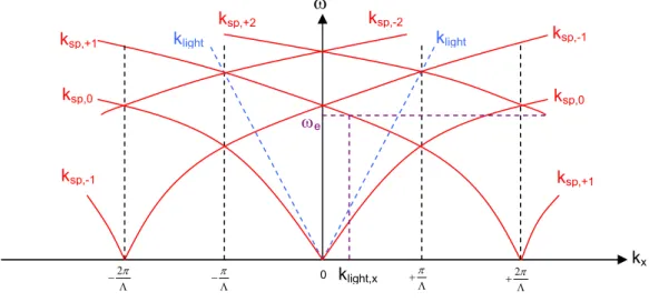
Figure 2.3 shows the plasmonic dispersion relation for grating coupling.
Figure 2.3: The plasmonic dispersion relation for grating coupling. 0 +π Λ 2π + Λ π − Λ 2π − Λ klight,x ωe klight ksp,-1 ksp,-2 ksp,0 ksp,+1 ksp,+2 ksp,+1 ksp,0 ksp,-1 klight kx ω
10
Chapter 3
Optimization, Fabrication and
Characterization of SPR Gratings
Efficient coupling of excitation light to surface plasmons is desirable in SPR based sensing applications. This chapter outlines our effort on obtaining high-efficient grating couplers both numerically and experimentally.
3.1 Optimization of Gratings
Optimization of grating couplers via numerical methods including finite element method (FEM) [21], finite-difference time domain (FDTD) [22] dyadic Green’s tensor method and rigorous coupled wave analysis (RCWA) [23] has been discussed in the previous works. RCWA is proposed as a successful and accurate method for the analysis of the diffraction of electromagnetic waves by periodic structures. [24] In this study, we introduce our results on the numerical optimization of silver coated gratings in air medium based on RCWA. Complex permittivity data is supplied from Palik’s Handbook of Optical Constants of Solids. [25]
3.1.1 Geometric Parameters
Main geometric properties of a grating to be optimized are periodicity, surface profile, groove depth and duty cycle.
• Periodicity: Surface plasmon excitation wavelength λe and resonance
angle θR pair is approximately derived from the grating coupling
equation depending on the grating period Λ and dielectric constants of the surrounding dielectric media, εd and the metallization, εm. In
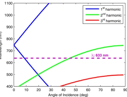
the case of a silver grating in air medium, Λ is found as 740 nm and 545 nm for the +1st and -1st diffracted orders, respectively, for λe=633
nm and θR=8.8 deg as shown in Fig.3.1. Due to the fabrication
considerations which are explained in Chapter 3.2.1, Λ is set as 740 nm for the following numerical calculations.
CHAPTER 3. OPTIMIZATION, FABRICATION AND 11 CHARACTERIZATION OF SPR GRATINGS 0 5 10 15 20 25 30 400 500 600 700 800 900 1000 1100
Angle of Incidence (deg)
Wavelength (nm) +1st order −1st order λ: 633 nm +1st order −1st order Λ: 740 nm Λ: 545 nm
Figure 3.1: Dispersion curves of a silver coated grating in air medium for grating periods of Λ=740 nm and Λ=545 nm
• Surface profile: Sinusoidal and non-sinusoidal gratings are simulated in order to reveal the effect of spatial harmonics on the reflectivity spectra with respect to the angle of incidence. Grating coupling equation estimates resonance angles as θR,1=8.8 and
θR,2=44.6 degrees for the first and second spatial harmonics,
respectively, at SPP excitation wavelength of 633 nm for a silver grating with Λ=740 nm (Fig.3.2). More accurate resonance angles are obtained by RCWA as θR,1=10.3 and θR,2=42 degrees (Fig.3.3). Since
sinusoidal grating has no higher spatial harmonics and lamellar grating has no even higher spatial harmonics, there exists no resonance curve around θR,2=42 deg. However, we see plasmonic
resonances for sawtooth and arbitrarily defined gratings around θR,2=42 deg due to the existence of even spatial harmonics in addition
to odd spatial harmonics. Indeed, we deal with the sharpness of the resonance curves and use angular quality factor as a measure of the sharpness which is defined as the ratio of the resonance angle and FWHM angle. Sinusoidal, sawtooth and arbitrary gratings are found to have angular Q-factors varying between 17 and 22 whereas lamellar grating has a lower angular Q-factor around 9.
Higher spatial order resonance curves offer additional resonance angles at a constant excitation wavelength. However, angular Q-factor reduction due to the intersection and broadening of the resonance curves at an interval of certain excitation wavelengths
CHAPTER 3. OPTIMIZATION, FABRICATION AND 12 CHARACTERIZATION OF SPR GRATINGS
should be carefully treated (Fig.3.4). For the case of the arbitrary grating which has both even and odd spatial harmonics, angular Q-factor decreases from 13 to 9 for the excitation wavelengths of 550 nm and 529 nm, respectively (Fig.3.5). On the other hand, angular Q-factor slightly reduces to 12.24 for the excitation wavelength of 522 nm even the peak reflectivity rises up above 0.64.
Figure 3.2: Dispersion curves of the first and higher spatial harmonics of a silver grating in air medium for grating period of Λ=740 nm
Figure 3.3: Reflectivity spectrum with respect to the angle of incidence for various grating profiles.
CHAPTER 3. OPTIMIZATION, FABRICATION AND 13 CHARACTERIZATION OF SPR GRATINGS
Figure 3.4: Dispersion curves of an arbitrary grating which has both even and odd spatial harmonics. (Λ=740 nm)
15 20 25 30 0 0.1 0.2 0.3 0.4 0.5 0.6 0.7 0.8 0.9 1
Angle of Incidence (deg)
Reflectivity
λ: 550 nm λ: 529 nm λ: 522 nm
Figure 3.5: Angular Q-factor reduction due to the intersection and broadening of the first and second spatial harmonic resonance curves.
CHAPTER 3. OPTIMIZATION, FABRICATION AND 14 CHARACTERIZATION OF SPR GRATINGS
• Groove depth: RCWA simulations reveal that peak reflections strongly depend on the groove depth (Fig.3.6). 45 nm depth is found as the optimal depth for a sinusoidal silver grating in air. Substantial Q-factor reduction as much as 60%’s is observed as the groove depth is set from 45 nm to 90 nm (Fig.3.7).
Figure 3.6: Peak reflectivity as a function of the groove depth. (λe=633 nm,
Λ=740 nm)
Figure 3.7: Reflectivity spectrum with respect to the angle of incidence for various groove depths.
CHAPTER 3. OPTIMIZATION, FABRICATION AND 15 CHARACTERIZATION OF SPR GRATINGS
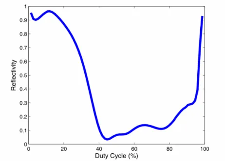
•
Duty cycle: Duty cycle (ratio of the ridge width to the grating period)of a lamellar grating is also found to be as a critical parameter as the groove depth (Fig.3.8). Duty cycles around 50% are found to be optimal. Resonance angle shifts are observed in addition to the angular Q-factor reduction depending on the duty cycle (Fig.3.9).
Figure 3.8: Peak reflectivity as a function of the duty cycle. (λe=633 nm, Λ=740
nm)
Figure 3.9: Reflectivity spectrum with respect to the angle of incidence for various duty cycles.
CHAPTER 3. OPTIMIZATION, FABRICATION AND 16 CHARACTERIZATION OF SPR GRATINGS
3.1.2 Metallization Parameters
Main metallization parameters to be optimized are thickness and material.
• Thickness: Metal layers are coated on gratings made of a different material. As the metal film gets thinner, optical properties of the sublayer may not be neglected anymore. Normalized intensities of reflectance, transmittance and absorbance as a function of the thickness of silver coating on a sublayer with the refractive index of ns=1.45 are numerically
calculated (Fig.3.10). As the non-reflected intensity is transmitted rather than absorbed due to thinner metallization, broadening in the reflected intensity curve is observed (Fig.3.11 and Fig.3.12). Thicknesses above 100 nm are found to be safe for silver coated gratings with 60 nm depth.
Figure 3.10: Normalized intensities of reflectance, transmittance and absorbance as a function of the thickness of silver coating. (λe=633 nm, Λ=740 nm)
CHAPTER 3. OPTIMIZATION, FABRICATION AND 17 CHARACTERIZATION OF SPR GRATINGS
Figure 3.11: Normalized intensities of reflectance, transmittance and absorbance with respect to the angle of incidence for a silver coated grating with the thickness of tAg=120 nm on a sublayer with the refractive index of ns=1.45.
Figure 3.12: Normalized intensities of reflectance, transmittance and absorbance with respect to the angle of incidence for a silver coated grating with the thickness tAg=35 nm on a sublayer with the refractive index of ns=1.45.
CHAPTER 3. OPTIMIZATION, FABRICATION AND 18 CHARACTERIZATION OF SPR GRATINGS
• Material: Material of the metallization is obviously one of the most fundamental parameters of grating coupled SPR as can be deduced from grating coupling equation. At excitation wavelength of 633 nm, silver coating is found to yield the sharpest resonance curves as compared with the aluminum and gold coatings (Fig.3.13).
Figure 3.13: Reflectivity spectrum with respect to the angle of incidence for various metal coatings. (λe=633 nm, Λ=740 nm)
CHAPTER 3. OPTIMIZATION, FABRICATION AND 19 CHARACTERIZATION OF SPR GRATINGS
3.2 Fabrication of Gratings
3.2.1 Nanoimprint Lithography
Quasi-sinusoidal gratings are fabricated using nanoimprint lithography as shown schematically in Fig.3.15. We prepare master molds from commercial optical discs by applying some chemical and physical procedures [26]. Corrugations near the edges of such discs are well approximated by gratings with a period of Λ=1540 nm for CD-R, Λ=740 nm for DVD-R and Λ=340 nm for Blu-Ray. The rewritable discs generally use a hard chalcogenide material as the recording medium (CD-RW and DVD-RW) and Blu-Ray write-once discs also use a multilayer hard coating. However, the write-once CD-R and DVD-R discs use a dye layer as the recording medium that can be dissolved in weaker solvents. Therefore, we focus on the write-once discs. For the case of the DVD-R discs, due to the thick layers that protect the recording layer, the inner surface was exposed by first mechanically cutting a notch into the side of the disc and then by applying mechanical force to peel the two sides apart. The initial cut provides a location for separation, which can be initiated by a sharp cutter. After peeling off the top surface, the dye layer was washed repeatedly in isopropanol. This procedure was observed not to change the disc corrugation but completely remove the dye. After cleaning, a 4:1 mixture of isopropanol and acetone was used to etch the grating to the desired depth. Typical etch times were from 10 seconds to a few minutes. Slight agitation during etching was observed to be important for uniform and repeatable etching. In the case of CD-R, the top protective layer was peeled off by exfoliation using a tape after delineation of the surface with a sharp cutter. The same procedure that was used for the DVD-R was also used for cleaning and etching of the CD-DVD-R discs. The effect of etching on the topography of disc surfaces are measured using atomic force microscopy (PSIA XE100) as shown in Fig.3.14.
Figure 3.14: Topographic profiles of the gratings obtained by Atomic Force Microscopy as a function of etching time on optical discs. (a) Modified DVD-R disc surface profiles with Λ=740 nm. (b) Modified CD-R disc surface profiles with Λ=1540.
CHAPTER 3. OPTIMIZATION, FABRICATION AND 20 CHARACTERIZATION OF SPR GRATINGS
Having modified DVD-R as master mold, liquid polydimethylsiloxane
(PDMS) (Sylgard 184, Dow Corning) is poured on and cured at 70 °C during 5 hours (Fig.3.15). After curing, elastomeric stamp is peeled off from the master mold. As the grating material, a photoresist (AZ5214, AZ Electronic Materials) is diluted 1:3 by a photoresist thinner (AZ1500 Thinner, AZ Electronic Materials) and spin-coated at 8000 rpm. Elastomeric stamp is released softly on the thinned photoresist film and hard-baked on the hotplate at 120 oC about 5 minutes. At last, stamp is mechanically removed from the sample. AFM image of sine-like polymeric grating is shown in Fig.3.16.
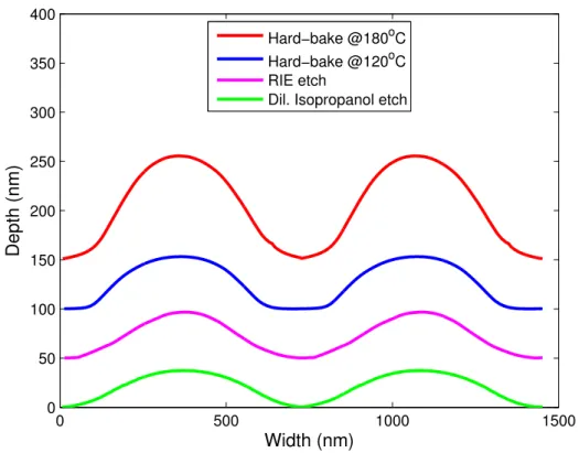
Further adjustment of the groove depth to some degree keeping the profile of the polymeric grating almost unchanged is possible (Fig.3.17). Hard-baking at a higher temperature than 120 oC results deeper gratings. For our case, hard-baking at 180 oC yields 100 nm depth whereas hard-baking at 120 0C yields 55 nm depth. In order to get shallower surfaces, diluted isopropanol etch or O2
plasma treatment may be applied. Groove depth is reduced from 55 nm to 35 nm by 2:1 IPA:DI wet etch for 6 min and 45 nm by reactive ion etching (RIE) O2
plasma etch for 1 min at 100W RF power. However, wet etching gives smoother surfaces than dry etching.
Unfortunately, polymeric gratings suffer from KOH etch process which has to be used latter to release micromembranes even metal-coated by either sputtering or thermal evaporation. Adding one more step, we have transferred grating patterns from thin polymer film to the underlying SiNx layer by fluorine based reactive ion etching (Fig.3.18). CHF3:O2 plasma etches both SiNx and
thinned photoresist with a higher etch rate of SiNx. Surface profile of the polymeric grating is almost conserved during the RIE etching until the SiNx sublayer is reached due to the high vertical directionality of RIE etch and low thickness of the photoresist film. As SiNx layer is reached, both photoresist and SiNx layers are etched together. The more photoresist is etched vertically, the more SiNx layer is subject to the plasma etchants laterally. As a result, grating profile is transferred from the polymer to the SiNx layer with depth multiplied by approximately the ratio of the etch rates. AFM images of the resulting SiNx gratings are shown in Fig.3.19. Similar to the previous case, further surface modification is possible to tune the groove depth. 1:2560 HF:DI etch for 10 min reduces the groove depth from 120 nm to 85 nm Fig.3.20.
CHAPTER 3. OPTIMIZATION, FABRICATION AND 21 CHARACTERIZATION OF SPR GRATINGS
Figure 3.15: Fabrication steps of the polymeric gratings using nanoimprint lithography. (a) Surface modified DVD-R disc with sine-like profile is used as master mold. (b) PDMS is poured on the master mold and cured at 70 0C for 5h. (c) Cured PDMS is peeled off from the master mold and used as elastomeric stamp. (d) Thinned photoresist is spin-coated on SiNx deposited substrate. (e) Elastomeric stamp is released gently on the thin polymer film and hard-baked to make polymer hardened. (f) Elastomeric stamp is mechanically removed from the sample.
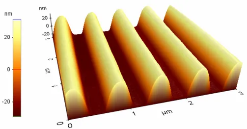
Figure 3.16: AFM topography image of the sine-like nanoimprinted polymeric grating
CHAPTER 3. OPTIMIZATION, FABRICATION AND 22 CHARACTERIZATION OF SPR GRATINGS 0 500 1000 1500 0 50 100 150 200 250 300 350 400 Width (nm) Depth (nm) Hard−bake @180oC Hard−bake @120oC RIE etch
Dil. Isopropanol etch
Figure 3.17: Topographic profiles of the polymeric gratings with different groove depths
Figure 3.18: Schematic representation of polymer-to-SiNx grating pattern transfer process using fluorine based reactive ion etching
CHAPTER 3. OPTIMIZATION, FABRICATION AND 23 CHARACTERIZATION OF SPR GRATINGS
Figure 3.19: AFM topography image of the sine-like SiNx grating
0 100 200 300 400 500 600 700 800 0 20 40 60 80 100 120 140 Width (nm) Depth (nm) Photoresist SiNx Dil. HF etch
CHAPTER 3. OPTIMIZATION, FABRICATION AND 24 CHARACTERIZATION OF SPR GRATINGS
3.2.2 Electron Beam Lithography
Lamellar SiNx gratings are fabricated using electron beam lithography (FEI
Nova NanoSEM 600). Two alternative processes are used: (a) Cr etch process and (b) Cr lift-off process (Fig.3.21). At process (a), chromium etch mask is defined by chromium etching. First, 50 nm chromium is sputtered on PECVD (plasma-enhanced chemical vapor deposition) growth SiNx film. Electron beam
lithography resist poly (methyl methacrylate) (PMMA) is spin-coated and
pre-baked at 180 oC for 2 minutes. 740 nm period linear gratings are defined by
electron beam exposure. PMMA is developed in 1:3 methyl isobutyl ketone
(MIBK): isopropyl alcohol (IPA) developer solution. Chromium is wet etched in
1:5 diluted Cr etchant (CR-7S, Cyantek) for 1 min. SiNx is then dry etched by
RIE CHF3:O2 plasma. Chromium mask is removed at the end and we are left
with lamellar SiNx gratings. At process (b), chromium etch mask is defined by lift-off process. First, PMMA is spin coated and pre-baked as in the previous case. After PMMA develop, chromium is sputtered on. PMMA mask is removed in ultrasonic acetone bath. Chromium sputtered on the PMMA are lifted-off and the same RIE etch procedure is followed. It should be noted that lift-off process has superiorities over the other process. First, wall profiles of the Cr mask is undoubtedly better such that Cr mask itself may be used as the grating excluding the RIE etch process. Second, it does not suffer from overetches which may lower the duty cycle. On the other hand, PMMA film has to be sufficiently thicker than the Cr film for the lift-off process to occur. Atomic force microscopy and scanning electron microscopy images of lamellar SiNx gratings fabricated using the second process are shown in Fig.3.21.
Exposure parameters should be optimized on some dummy samples before starting the fabrication of desired structures. Dose matrix process is employed for this purpose. In this process, a matrix of mask elements with steadily increasing exposure dose values is prepared and exposed to a dummy sample. Standard procedures for developing the PMMA are followed and according to the PMMA mask patterns imaged by usual scanning electron microscopy, the best fitting dose values are determined. For our case, at 10 kV beam voltage and
150 pA measured beam current, 100 mJ/cm2.sec gives the optimal results. Also
exposure resolution which is basically limited by the interface electronics between the lithography instrument and the control PC is an important parameter. 20 nm spatial resolution is found to produce satisfactorily smooth grating patterns with Λ=740 nm.
CHAPTER 3. OPTIMIZATION, FABRICATION AND 25 CHARACTERIZATION OF SPR GRATINGS
Figure 3.21: Fabrication steps of lamellar SiNx gratings. (a) Chromium etch process. (a.1) 740 nm period linear gratings are defined by electron beam exposure. (a.2) PMMA is developed and chromium is wet etched in diluted Cr
etchant. SiNx is dry etched by RIE CHF3:O2 plasma. (a.3) Chromium mask is
removed. (b) Chromium lift-off process. (b.1) Similar to (a.1) except there is no Cr layer initially. (b.2) Chromium sputtered on PMMA mask and lifted-off. (b.3-4) Same as the (a.2-3) (c) AFM topography image of lamellar SiNx gratings. (d) SEM image of lamellar SiNx gratings with thin Au/Pd coating.
3.2.3 Optical Lithography
Lamellar gratings with periods of Λ=3µm are fabricated using optical lithography (Fig.3.22). A positive photosensitive polymer (AZ5214) is
spin-coated at 5000 rpm on the PECVD growth SiNx layer and pre-baked at 110 oC
for 50 secs. UV light is exposed through a UV and visible-transparent mask (like quartz or glass) having opaque chromium grating patterns. Exposed regions are developed in 1:4 AZ400K:DI for 30 secs. Photoresist etch mask is then
post-CHAPTER 3. OPTIMIZATION, FABRICATION AND 26 CHARACTERIZATION OF SPR GRATINGS
baked at 120 oC for 2 minutes for good stiction during the wet etch process.
SiNx is wet etched in diluted HF and the remaining photoresist is removed by applying acetone and isopropanol.
In the case of lamellar grating fabrication, optical lithography duration is substantially shorter than electron beam lithography duration of the same size pattern. However, minimum feature size achievable using optical lithography is inherently limited by the diffraction of the light and is practically about sub-microns. Hence, only groove periods on the order of micrometers can be defined using this lithographic technique. Micron period gratings are appropriate for the excitation of surface plasmons at IR wavelengths.
Figure 3.22: Fabrication steps of 3 µm period lamellar SiNx gratings using optical lithography. (a.1) A positive photosensitive polymer on the PECVD growth SiNx layer and pre-baked . (a.2) UV light is exposed through a grating mask. (a.3) Exposed regions are developed and photoresist mask is post-baked. (a.4) SiNx is wet etched in diluted HF and the remaining photoresist is removed by applying acetone and isopropanol. (b) Scanning electron micrograph of 3 µm period lamellar SiNx gratings
CHAPTER 3. OPTIMIZATION, FABRICATION AND 27 CHARACTERIZATION OF SPR GRATINGS
3.3 Characterization of Gratings
Topographic and plasmonic properties of silver coated gratings are characterized using atomic force microscopy and variable angle spectroscopic ellipsometry (V-VASE, J.A. Woollam), respectively. AFM topography images reveal the exact profile of silver coated gratings (Fig.3.24). A representative line profile which is averaged over a wide area is imported to RCWA simulation as the real grating profile while generating the numerical dispersion diagram. Experimental dispersion diagram is obtained by measuring the p-polarized reflected intensity with respect to both excitation wavelength and angle of incidence. Numerical and experimental results are observed to be in good agreement (Fig.3.25). θFWHM’s below 1 deg is achieved as estimated by the numerical analysis.
Spectroscopic scan measurement of another silver coated grating is also provided to show the polarization dependence of the SPP excitation in the grating coupling scheme. In the spectroscopic scan, Ψ and ∆ are measured which are given by,
tan( ) p i s r e r ∆ = Ψ
where rpand rsare the normalized amplitudes of s and p components of the reflected light. Since surface plasmons are excited by only p components, Ψ diminishes and ∆ shifts by 90 degrees at the resonance angles (Fig.3.26).
Figure 3.23: Elliptically polarization of the linearly polarized beam upon reflection
CHAPTER 3. OPTIMIZATION, FABRICATION AND 28 CHARACTERIZATION OF SPR GRATINGS
Figure 3.24: Topographic characterization of a silver coated grating. (a) AFM topography image. (b) A representative line profile.
CHAPTER 3. OPTIMIZATION, FABRICATION AND 29 CHARACTERIZATION OF SPR GRATINGS
Angle of Incidence (deg)
Wavelength (nm) 15 20 25 30 500 510 520 530 540 550 560 570 580 590 600 0 0.1 0.2 0.3 0.4 0.5 0.6 0.7 0.8 0.9 1
a)
Angle of Incidence (deg)
Wavelength (nm) 15 20 25 30 500 510 520 530 540 550 560 570 580 590 600 0.1 0.2 0.3 0.4 0.5 0.6 0.7 0.8 0.9 1
b)
Figure 3.25: Plasmonic characterization of a silver coated grating (same as given in Fig.3.24). (a) Experimental dispersion curves (interpolated). (b) Numerical dispersion curves.
CHAPTER 3. OPTIMIZATION, FABRICATION AND 30 CHARACTERIZATION OF SPR GRATINGS
Angle of Incidence (deg)
Wavelength (nm) 15 20 25 30 500 510 520 530 540 550 560 570 580 590 600 10 15 20 25 30 35 40 45
a)
Angle of Incidence (deg)
Wavelength (nm) 15 20 25 30 500 510 520 530 540 550 560 570 580 590 600 90 100 110 120 130 140 150 160 170 180
b)
Figure 3.26: Spectroscopic scan measurements of a silver coated grating. (interpolated) (a) ψ with respect to the wavelength and the angle of incidence. (b) ∆ with respect to the wavelength and the angle of incidence.
31
Chapter 4
Angular Displacement Detection
Method
A new angular displacement detection method based on surface plasmon resonance is proposed. Two alternative designs are investigated as illustrated in Fig.4.1. Excitation light is incident at a bias angle maximizing the signal-to-noise ratio. Reflected or transmitted beam intensities are detected by a photodetector in single or double grating designs, respectively. Resonant transmission of light through the double grating structure is recently discussed. [27] Angular displacement is detected through the photocurrent change depending on the intensity change associated with the plasmonic excitation.
Figure 4.1: Illustration of the surface plasmon resonance based angular displacement detection schemes. (a) Single grating with thick metallization to read the reflected beam intensity at the same side with the light source. (b) Double grating with thin metallization to read the transmitted intensity at the opposite side of the light source
The photodetector current is given by
i
pd= ℜ
P
where P is the power of the incident beam upon the photodetector andℜ
is the spectral responsivity of the photodetector. The spectral responsivity is given by qhc η λ
ℜ =
where η is the quantum efficiency, q is the charge for one electron,λ
is the wavelength, h is theCHAPTER 4. ANGULAR DISPLACEMENT DETECTION METHOD 32
Planck’s constant and c is the speed of light. For a silicon pin photodiode,
0.41
ℜ ≈
A/W forλ
=633 nm andℜ ≈
0.69
A/W forλ
=950 nm assuming that the quantum efficiency is η =0.9. Photon shot noise current which arises due to the random arrivals of the photons to the photodiode is expressed as2
2
sh qi Bpd
i
=
where B is the measurement bandwidth in hertz. Shot noise equivalent angular displacement (SNEAD) may be considered as the minimum detectable angular displacement for our detection scheme as like other optical detection schemes. The angular sensitivity is defined asS
ipdθ
∂ ∂
=
whereθ
is the angle of incidence. SNEAD is evidently found as2 2 sh sh pd i i
θ
θ
∂ ∂ =
(4.1)Intensity of the incident beam as a function of the angle of incidence is numerically calculated using RCWA (Fig.4.2). As a first order approach, the photodetector current as a function of the angle of incidence ignoring the spectral width,
∆
λ
and beam divergence,β
of the light source, is expressed as( )
( ,
e) ( )
epd
i
θ
=
P
θ λ
ℜ
λ
(4.2)where
λ
eis the SPP excitation wavelength of the incident beam. Figure 4.3 shows calculated SNEAD as a function of the excitation wavelength for a silicon pin photodiode. Nanoradian per root hertz SNEAD is found to be achievable for a 1mW light source. 0,0 0,1 0,2 0,3 0,4 10 -8 10 -7 10 -6 10 -5 10 -4 10 -3 10 -2 10 -1 10 0 (a) F r a c t i o n o f t r a n s m i t t e d p o w e r , P i / P tAngle of incidence (rad) TM Order 1 TM Order 0 TM Order -1 0,0 0,1 0,2 0,3 0,4 10 -8 10 -7 10 -6 10 -5 10 -4 10 -3 10 -2 10 -1 10 0 (b) F r a c t i o n o f t r a n s m i t t e d p o w e r , P i / P t
Angle of incidence (rad)
TM Order 1 TM Order 0 TM Order -1
Figure 4.2: Fraction of transmitted powers, Pi/Pt with respect to the angle of incidence for TM beams with excitation wavelengths of λe=633 nm (a), and (b)
CHAPTER 4. ANGULAR DISPLACEMENT DETECTION METHOD 33 400 500 600 700 800 900 1000 10 -10 10 -9 10 -8 10 -7 10 -6 10 -5 0,0 0,2 0,4 0,6 0,8 1,0 SNEAD S hot noi s e e qui v a l e nt a ng ul a r di s pl a c e m e nt ( r a d/ Hz 1 / 2 ) Wavelength (nm) Spectral sensitivity S p e c t r a l s e n s i t i v i t y
Figure 4.3: Shot noise equivalent angular displacement with respect to the excitation wavelength of the incident beam for a commercial silicon PIN photodiode having the plotted spectral sensitivity
In a more realistic case with light sources having non-zero spectral widths, the photodetector current is approximated by
max min ( )
( , ) ( )
pdi
P
d
λ λθ
≈∫
θ λ
ℜ
λ λ
(4.3) Figure 4.4.a shows calculated SNEAD as a function of the angle of incidence for various selected spectral widths. SNEAD rises up by 2 orders of magnitude asλ
∆
is increased from 5 nm to 80 nm.In another realistic case with light sources having non-zero beam divergence angles, the photodetector current is approximated by
max min ( )
( )
e(
,
e)
pdi
P
d
α αθ
≈ℜ
λ
∫
θ α λ α
−
(4.4)Figure 4.4.b shows calculated SNEAD as a function of the angle of incidence for various selected beam divergence angles. 3 orders of magnitude increase in SNEAD is observed as
β
is expanded from 3 mrad to 300 mrad.CHAPTER 4. ANGULAR DISPLACEMENT DETECTION METHOD 34 0,0 0,1 0,2 0,3 0,4 10 -9 10 -8 10 -7 10 -6 10 -5 (a) S N E A D ( r a d / H z 1 / 2 )
Angle of incidence (rad) =5 nm =20 nm =80 nm 0,0 0,1 0,2 0,3 0,4 10 -9 10 -8 10 -7 10 -6 10 -5 10 -4 (b) S N E A D ( r a d / H z 1 / 2 )
Angle of incidence (rad) =3 mrad
=30 mrad =300 mrad
Figure 4.4: Shot noise equivalent angular displacements with respect to the angle of incidence for realistic cases. (a) For various spectral widths. (b) For various beam divergence angles.
35
Chapter 5
Design, Fabrication and
Characterization of MEMS Devices
5.1 Theoretical Background
5.1.1 Beam Theory
The dynamic behavior of beam resonators can be analyzed by Euler-Bernoulli theory.[28] The force balance on the infinitesimal section of an undamped beam is expressed as 2 2 2 2 2 2 ( , ) ( , ) ( , ) U y t U y t EI A F y t y y
ρ
t ∂ ∂ ∂ + = ∂ ∂ ∂ (5.1)where E is the Young’s modulus, I is the moment of inertia, ρ is the mass density, A is the cross-sectional area of the beam and ( , )F y t is the time-varying external load in the z-direction. In Figure 5.1, a doubly clamped beam loaded by
( , )
F y t at its fundamental mode is schematically depicted.
Figure 5.1: Fundamental mode shape of a doubly clamped beam resonator with length l , thickness h and width w. U y t( , ) is the position and time dependent displacement of the beam in the z-direction .
For a beam of rectangular cross-section with thickness h and width w, the cross-sectional area is A=hwand the moment of inertia is 1 3
12