Dipole Antenna Couplers for Subwavelength
Metal-Insulator-Metal Waveguides
M. Cengiz Onbasli1, Ali K. Okyay2,3
1 Department of Materials Science and Engineering, Massachusetts Institute of Technology, Boston, USA, MA 02139 2Department of Electrical and Electronics Engineering, Bilkent University, Ankara TR-06800, Turkey 3UNAM, National Institute for Materials Science and Nanotechnology, Bilkent University, Ankara TR-06800, Turkey
e-mail: [email protected], [email protected]
Abstract: Near-infrared light (λ=1550 nm) was coupled into a 100-nm-core Ag/SiO2/Ag
waveguide using dipole antennas. We demonstrate that using antennas, the field intensity inside the waveguide can be enhanced by changing the antenna size and location.
OCIS codes: 240.6680, 250.5403, 230.7370 1. Introduction
Metal-insulator-metal (MIM) waveguides have been investigated extensively in the recent literature due to sub-wavelength localization of electromagnetic radiation by plasmon modes [1-3]. Sub-sub-wavelength confinement combined with wide bandwidth capability [4,5], make MIM waveguides very attractive for high sensitivity spectroscopy applications, and biosensing [6,7], waveguiding [3], nonlinear optical phenomena [8,9] and on-chip signal routing, modulation and processing [10-12]. Copper interconnects used today are (i) bulky and (ii) cannot be integrated at high density due to increasing power dissipation per area and (iii) RC delays of copper lines limit operation bandwidth [13]. Optical waveguides can serve to circumvent the second and third limitation of copper interconnects. In order to achieve sub-wavelength localization and reach even higher density interconnects, plasmonic waveguiding through the MIM topology has been proposed [1,2].
MIM waveguides suffer from high attenuation especially in the visible spectrum due to strong losses at the metal claddings. It is possible to achieve compensation of dissipative loss by incorporation of gain medium as the insulating core and lasing through the core has been achieved [8]. In order to increase the propagation distance, research efforts focused on the optimization of the MIM waveguide architecture [3,5,14]. Most of such work focuses on the optimization of the electromagnetic modes inside the MIM structure. However, there are limited reports on the coupling of external electromagnetic radiation into the MIM waveguide. Most research in that area focuses on the use of a type of a tapered architecture combined with a grating coupler that precedes the taper [15,16]. Therefore, it is necessary to introduce effective coupling methods from micron-size fibers to the waveguides of a few hundred nanometers in size.
In this study, we propose and simulate dipole antenna-MIM waveguide system to show that simple dipole antennas can be integrated with MIM waveguides to achieve (i) enhanced coupling into the MIM waveguide, and (ii) tune the mode field intensity profile inside the silicon oxide core by changing the antenna length, antenna width and the antenna-waveguide separation.
2. Simulation
Two dimensional finite difference time domain simulations of combined antenna-waveguide structures were carried out using commercial software, Lumerical FDTD Solutions [17]. 2D simulations were preferred to 3D simulations for (i) reducing numerical memory and computational time requirements. Earlier work on the propagation distance versus waveguide parameters show that the propagation length no longer increases for waveguides thicker that 250 nm [3, Figures 4b and 6b]. A baseline waveguide was assumed and kept unchanged throughout the analysis. The MIM structure was assumed to be free standing in free space and it consists of 100-nm-wide silver claddings and 100-nm-wide SiO2 core, as shown in Figure 1. Both TE and TM incident plane waves were simulated for the range of λ = 1300 nm to λ = 1600 nm. The top and bottom silver cladding thicknesses were set at 100 nm with a 100-nm-thick SiO2 layer. We systematically varied the dipole antenna coupler structure in front of the baseline Ag/SiO2/Ag waveguide. The antenna arm length (along +y direction) was varied from 50 to 700 nm, arm width (along +x direction) was varied between 20 to 150 nm and antenna-waveguide separation was varied from zero (connected) to 150 nm.
a1070_1.pdf
FWU5.pdf
© 2010 OSA /FiO/LS 2010
FWU5.pdf
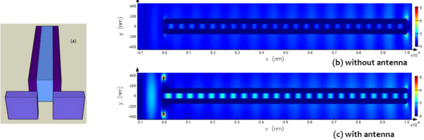
Fig. 1. (a) Schematics of the waveguide and the antenna structure. (b) E-field intensity profile for the waveguide without antenna (λ = 1600nm) (c) E-field intensity profile for antenna of 300 nm length, 50 nm width, connected to the waveguide (λ = 1600 nm). The antenna confines the energy inside the waveguide by increasing the effective aperture area of the input facet of the waveguide. All intensities are linear and normalized
with respect to source (Fig. 1c’s upper limit was scaled down from 14 to 9).
3. Results and Discussion
When the dipole antenna is disconnected from the MIM structure, a strong field confinement is obtained at the gap between the coupler and the antenna. This is due to the interaction between the modes of the antenna and the waveguide aperture. A limited amount of this mode is coupled into the waveguide since the near-field radiation pattern of the disconnected antenna strongly couples with the cladding edges. This cannot initiate strong surface plasmon modes within the waveguide, but instead, in the gap between the antenna arms and the waveguide. The angular distribution of the antenna emission pattern cannot induce as much surface charges at the interfaces as in the connected antenna case (i.e. the overlap integral of the surface plasmon modes and the emission pattern is smaller than that in the connected antenna case). When the antenna structure is connected to the waveguide, a very strong coupling is observed, effectively increasing the acceptance cross-section of the waveguide. Efficient coupling was obtained as demonstrated in Figure 1b and 1c, showing the field amplitudes inside the MIM structure with a dipole antenna coupler and without one. The E-field intensity inside the core is enhanced more than 5 times, varying with the antenna dimensions.
4. References
[1] Dionne, J. et. al., “Silicon-Based Plasmonics for On-Chip Photonics”, IEEE Journal of Selected Topics in Quantum Electronics, Vol. 16, No. 1, pp. 295- 306, January/February 2010
[2] Dionne, J. et. al., “Plasmon slot waveguides: Towards chip-scale propagation with subwavelength-scale localization”, Physical Review B 73, 035407 (2006)
[3] Veronis, G.; Fan, S.; “Modes of Subwavelength Plasmonic Slot Waveguides”, Journal of Lightwave Technology, Vol. 25, No. 9, Sept. 2007 2511
[4] S. E. Kocabas, G. Veronis, D. A. B. Miller, and S. H. Fan, “Modal Analysis and Coupling in Metal-Insulator-Metal Waveguides,” Phys. Rev. B 79, 035120 (2009)
[5] R. F. Oulton, V. J. Sorger, D. A. Genov, D. F. P. Pile & X. Zhang, “A hybrid plasmonic waveguide for subwavelength confinement and long-range propagation”, Nature Photonics 2, 496 - 500 (2008)
[6] P. Berini, Bulk and surface sensitivities of surface plasmon waveguides, New Journal of Physics 10 (2008) 105010
[7] K.M. Evenson, D.A. Jennings, K.R. Leopold, and L.R. Zink, “Tunable Far Infrared Spectroscopy”, Appl. Phys. Lett. 44 (6). 15 March 1984 [8] M. T. Hill, M. Marell, E. S. P. Leong, et. al., “Lasing in metal-insulator-metal sub-wavelength plasmonic waveguides”, Optics Express, 17, 13, pp. 11107-11112 (2009)
[9] Zongfu Yu, Georgios Veronis, Shanhui Fan, M. L. Brongersma, “Gain-induced switching in metal-dielectric-metal plasmonic waveguides”, Applied Physics Letters 92, 041117 (2008)
[10] D. K. Gramotnev, S. I Bozhevolnyi, Nature Photonics, Vol. 4, Feb. 2010, 83 [11] S. I Bozhevolnyi, Nature Photonics, Vol. 440, 23 March 2006, 508
[12] S. I Bozhevolnyi ed., Plasmonic Nanoguides and Nanocircuits (Pan Stanford Publishing, 2008)
[13] D. A. B. Miller, "Physical Reasons for Optical Interconnection," Special Issue on Smart Pixels, Int’l J. Optoelectronics 11 (3), 155-168 (1997).
[14] Rashid Zia, Mark D. Selker, Peter B. Catrysse, and Mark L. Brongersma, JOSA A, 21, 12, 2442 – 2446 [15] Pavel Ginzburg, David Arbel, and Meir Orenstein, Optics Letters, 31, 22, (2006)
[16] S. Lardenois et. al., “Low-loss submicrometer silicon-on-insulator rib waveguides and corner mirrors”, Optics Letters, 28, 13, 1150-1152 (2003)
[17] Lumerical FDTD Solutions Inc., Suite 201 - 1290 Homer Street Vancouver, British Columbia, Canada V6B 2Y5
a1070_1.pdf
FWU5.pdf
© 2010 OSA /FiO/LS 2010