.Зг Зі/'З ё ; ■> 'ί - /л’- '■ ■■ s •Г·'· • ·Τ%2 л‘ ' і ш м і т т : -Ϊ .у*':-ѵ·.; ·.■^^-VJ ■■■/-' / ’ч;.'·' V /*-/Ѵ '.' * *'.-“Г> « Г л ' .*
•586
f 5 5 X . . » « t S iâ * ,E L E C T R O N IC S T R U C T U R E
OF S i/G e
S E M IC O N D U C T O R
S U P E R L A T T IC E S
A THESIS
SUBMITTED TO THE DEPARTMENT OF PHYSICS AND THE INSTITUTE OF GRADUATE STUDIES
OF BILKENT UNIVERSITY
IN PARTIAL FULFILLMENT OF THE REQUIREMENTS FOR THE DEGREE OF
MASTER OF SCIENCE
By
Oguz GULSEREN
Êjc
• su
c 3 9 * ? 2
I certify that I have read this thesis and that in my opinion it is fully adequate, in scope and quality as a dissertation for the degree of Master of Science.
Principal Advisor
I certify that I have read this thesis and that in my opinion it is fully adequate, in scope and quality as a dissertation for the degree of Master of Science.
Prof. Dr. Cemal Yalabık
I certify that I have read this thesis and that in my opinion it is fully adequate, in scope and quality as a dissertation for the degree of Master of Science.
A K. X
I certify that I have read this thesis and that in my opinion it is fully adequate, in scope and quality as a dissertation for the degree of Master of Science.
^ — y{/ i. — I
Assoc. Prof. Dr. Recai Eilialtioglu
I certify that I have read this thesis and that in my opinion it is fully adequate, in scope and quality as a dissertation for the degree of Master of Science.
Assoc. Prof. Dr. $inasi Ellialtioglu
Approved for the Institute of Graduate Studies
Director, Institute of Graduate Studies, Prof. Dr. Mehmet Baray
ABSTRACT
ELECTRONIC STRUCTURE OF Si/Ge
SEMICONDUCTOR SUPERLATTICES
G Ü L S E R E N , Oğuz M . S. in Physics
Supervisor : Prof. Dr. Salim Çıracı February 1988, 70 pages
A brief review about the two dimensional electron systems and especially band offsets is given. The electronic properties of the Si„/Ge„(001) strained superlattices as a function of the superlattice periodicity and the band misfit is investigated by using the empirical tight-binding method. The difference between the direct and indirect band gaps is reduced from 2.01 eV for bulk Si to 0.01 eV for n = 6. Consequently, the superlattice with n = 6 can be considered as quasi-direct, while it is at least 0.15 eV for n = 4 case. For the cases n=5,6, and 8, the band gap might become direct for large values of band misfit.
Key words : superlattices, band discontinuity, band line-up, band offset, strained superlattices, optical transition.
ÖZETÇE
Si/Ge YARIİLETKEN
SÜPERÖRGÜLERİNİN
ELEKTRONİK YAPISI
G Ü L S E R E N , Oğuz
Yüksek Lisans Tezi, Fizik Bölümü Tez Yöneticisi : Prof. Dr. Salim Çıracı
Şubat 1988, 70 satıife
İki boyutlu elektron sistemlerin özellikleri ve bant süreksizlikleri özetlendi. Si„/G e„(001) gerilimli süperörgülerin elektronik özellikleri süperörgü periyodu ve bant süreksizliği fonksiyonu olarak Denemesel Sıkı Bağlanma yöntemi kullanılarak incelendi. Doğrudan ve dolaylı bant aralıkları arasındaki fark, Si kristalinde 2.01 eV iken n = 6 için 0.01 eV’e düşmüştür. Bu durumda Sie/Gee süperörgüsü doğrudan bant yarıiletkeni olarak kabul edilebilir. Bu fark n = 4 için 0.15 eV’dir. n = 5,6, ve 8 durumları için, bant süreksizliğinin büyük değerlerinde bant aralığı doğrudan olabilir.
Anahtar sözcükler : süperörgüler, bant süreksizlikleri, gerilimli süperörgüler, optik geçişler
Acknowledgement
It is my pleasure to express deep gratitude to my supervisor, Prof. Salim Çıracı, for his guidance, suggestions and helps during the development of this study. I would like to thank to Assoc. Prof. Şinasi Ellialtioglu for his contributions to this work. I appreciate Erkan Tekman for his valuable discussions and comments. Lastly I would like to thank to Cemal Akyel and the Research Assistants of the Faculty for their continuous moral support.
Table of Contents
A b s t r a c t ... ii
Ö z e t ç e ... iii
Acknow ledgem ent... iv
Table of C o n t e n t s ... v
List of F i g u r e s ... vii
List of T a b le s ... ix
1 Introduction 1 2 Two Dimensional Systems and Band Line-ups 4 2.1 O v e r v ie w ... 4
2.2 Electronic S tr u c tu r e ... 7
2.3 Band L in e - u p s ... 10
2.3.1 Introductory R em a rk s... 10
2.3.2 Methods of Band Lineup Measurements... 11
2.3.3 Linearity and Transitivity... 17
2.3.4 Theory of Band L in e -u p s ... 18
2.4 G r o w t h ... 27
2.5 Device A p p lic a tio n s ... 29
2.6 Resonant T u n n e lin g ... 33
2.7 Quantized Hall Effect ... 34
2.8 Research A r e a s ... 36
3 Electronic Structure of Strained S i/G e Superlattices 38 3.1 Strained Si/Ge Superlattices ... 38
3.2 Empirical Tight-binding M e t h o d ... 42
3.3 Electronic Structure of Strained Sin/Ge„(001) Superlattices . . . 44
3.3.1 O v e r v ie w ... 44 3.3.2 The Method ... 45 3.3.3 Calculations... 47 4 Conclusions 58 References... 60 V I
List of Figures
2.1 Quantum well structure and real space energy band structure. . . 5 2.2 Discontinuities of band edge energies at four kinds of hetero
interfaces. ... 11 2.3 Energy band diagram for an abrupt Ge-GaAs heterojunction . . 12 2.4 XPS spectrum of (110) Ge-GaAs interface... 13 2.5 Absorption spectra for valence band to conduction band transitions 14 2.6 Absorption spectra (2K) of GaAs layers between Alo.2Gao.8As
b a r r ie r s ... 15 2.7 Schematic diagram of the electron affinity, the work function,
and the ionization e n e r g y ... 20 2.8 Experimental valence band offsets as a function of theoretical
valence band offsets calculated by Harrison... 23 2.9 Experimental valence band offsets of X /G e systems as a function
of theoretical valence band offsets calculated by Harrison... 24 2.10 A molecular beam epitaxy system ... 29 2.11 Energy band diagram for n-doped and undoped superlattices. . . 30 2.12 Energy band diagram of a staircase avalanche photodiode . . . . 32 2.13 Resonant tunneling model for heterostructures... 33
2.14 Hall resistance and electrical resistance of a GaAs/AlGaAs heteroj unction... 35
3.1 Energy gaps versus lattice constants at 4.2 K ... 39 3.2 Critical layer thickness as a function of alloy composition . . . . 40 3.3 Minimum band gap of GejjSii-x as a function of germanium fraction 41 3.4 Unit cell and Brillouin Zone of Sin/Ge„(001) superlattices . . . . 46 3.5 Variation of various gaps as a function of A E for the strained
Si4/Ge4(001) superlattice... 48 3.6 Energy band structures of Si8(001), Ge8(001) and Si4/Ge4(001)
structures... 49 3.7 Localization (weight in Si-sublattice) of the conduction and
valence band states of Si4/Ge4(001) as a function of A E . 52 3.8 Variation of various gaps as a function of A E for the strained
Si6/Ge6(001) superlattice... 55 3.9 Difference of energy between direct and indirect band gap for for
superlattice periodicity n as a function of A E ... 56
List of Tables
2.1 Valence band discontinuities at selected heterojunctions... 17 2.2 Valence band discontinuities including the dipole effects for
selected heterojunctions... 26
3.1 Gap values and Si-content of the wavefunctions at the Conduc tion Band minimum for various superlattice periodicities... 57
Chapter 1
Introduction
The two most important discoveries of our century are the transistor and the laser. Multivariable optimization problems, the requirement of high technology and high speed communications, created needs for high speed electronic devices coupled with laser sources.
The silicon based integrated circuits have been developed since second world war. The electronic industry based on these becomes the most important technology and business nowadays. In fact the silicon is a mediacor material. Although it has excellent etching and mechanical properties, it is an indirect gap semiconductor. Because of this silicon cannot be used in photonics and optoelectronics.
Research on GaAs has began because of its high mobility with respect to the silicon for fast devices and it is a direct gap material. Also interesting results have been obtained from the research on artificial layered structures or heterostructures such as lattice matched GaAs/Gai_a;Ala;As superlattice.
Properties of artificial layered structures depend on the dimensionality. The properties of a condensed system is strongly dependent on its dimensionality. Advances in growth techniques made it possible to produce various systems with lower dimensionality. Lower dimensionality means a system with an effective dimension less than three.
Introducing the two dimensional systems into various branches of science leads to new physical phenomena and thus broadens our insight. Both academic and technologically interesting problems are found. In two dimensional systems, electrons or holes are free to move in two directions and are confined in the third dimension.
The most important property of a semiconductor heterojunction is the band line-up. An energy discontinuity appears at the interface, since the valence band maximum does not correspond to the same point for the two materials. Band line-up determines the conduction and valence band discontinuities and hence the effective barrier for electron or hole transport across the interface. By the help of controlled growth techniques, energy band structure of the materials can be adjusted. Band gap engineering opens new options on device applications. It enables us to design the energy band diagram of a device and thus to control its electrical transport properties.
experiment was performed on a Si mosfet in which the electrons were free to carry current confined within a thin layer. Hall resistance showed a quantized character in terms of the fundamental constant h, the Planck’s constant. K. von Klitzing received the Nobel Prize in physics in 1985 because of his work on Quantized Hall effect.
Apart from the lattice matched semiconductor heterostructures, excellent techniques of superlattice growth have made the growth of dislocation-free, strained-layer superlattices involving thin layers of semiconductors with large lattice mismatch possible. New properties of Si/Ge strained superlattices are promising for silicon technology. Direct optical transitions were observed in Si4/G e4(001) superlattices, which are not found in constituent crystals.
In this thesis, the electronic properties of Sin/Ge„(001) superlattices have been investigated. Empirical tight binding method is used in band structure calculations of Sin/Ge„(001). The organization of the thesis is as follows: Chapter 2 concentrates on a review about the properties of two dimensional systems. Electronic structure of strained Si„/Ge„(001) superlattices is analysed in Chapter 3. First, the properties of strained-layer superlattices are introduced, then emprical tight-binding method is summarized. Also the results on the electronic structure of strained Si„/Ge„(001) superlattices is discussed. In Chapter 4, conclusions are presented.
Chapter 2
Two Dimensional Systems and
Band Line-ups
2.1
Overview
Two dimensional (2D) electron systems are the ones in which the components of the system are free to move in two spatial dimensions but have their motion constrained in the third dimension. In other words, the electrons or holes have quantized energy levels for one spatial dimension, but are free to move in two spatial dimensions. Thus the wave vector is a good quantum number for two dimensions, but not for the third [1].
As examples for 2D systems we can consider the junctions between insulatox's and semiconductors such as Si-Si02 interfaces, between vacuum and liquid helium and layered structures of semiconductors which are called superlattices [2] and those with continually varying compositions which are called graded-gap structures. In addition to these many other systems show
two dimensional character such as intercalated graphite and thin films. AIGaAs GaAs ^ 100 A GaAs substrate Energy levels > o tr Conduction band High-ef'ergy ba.nd gao Low-energy banc gap I — -.j- --- — r I [aE. ^ Valence band
\ /
Layer thicknessesFigure 2.1: Quantum well structure and real space energy band structure.
Layers of two or more compounds grown periodically one after another is shown in Figure 2.1. In real space there will be discontinuities in the energy bands as seen in Figure 2.1, since the layers have different band gaps. Quantization of the carrier motion in the direction perpendicular to the layers leads to a set of discrete energy levels. When the free electron behaviour along
the interface is included, the energy levels take the form
(2.1)
where and ky are the wave vector components for motion parallel to the surface and the En are the electronic quantum levels arising from confinement in the narrow potential well. Each value of En is the bottom of a two dimensional continuum called a subband. If the energy discontinuities are large enough and the layers with high energy band gaps are wide enough then there will be a little interaction between the layers with low-energy band gap. We can then analyse those layers seperately, that is the carriers confined in each one of those layers behave independently. So the results are quantum well structures. In the case of interaction between layers, which means the barriers are narrow or the energy of a state is comparable to the barrier height energy discontinuity, the wave functions of the carriers are extended perpendicularly to the layers. Therefore, the carriers axe modified by periodic long-range modulation of the crystalline potential. This periodic array is called the superlattice while one period is the heterostructure [3]. The superlattice periodicity creates a new, smaller Brillouin zone in the k^ direction. The discrete quantum levels of widely spaced wells are replaced by a series of energy bands called minibands. Their energy bandwidth increases as the barrier height and width decrease.
2.2
Electronic Structure
Electronic structure calculations are based on the effective mass approx imation. A free electron state with certain effective mass m* is used to study the motion of the electron parallel to the interface plane. For the motion perpendicular to the layers a potential arising from superlattice is taken into account.
Sham and Nakayama [4] studied the effective mass equation for an interface potential, actually in the space-charge layer in a MOSFET and in the n inversion layer of Si(100)-SiO2. Because of sharply varying interface potential, effective mass equation needs modification. They constructed a basis set of energy eigenfunctions of the inhomogeneous system including the interface under no external potential, so the interface boundary conditions are satisfied by the basis functions. Then electron wave function is expanded as a linear combination of the bulk eigenfunctions at the same energy. Combination includes the Bloch waves and evanescent waves at the same energy. After this, effective mass equations are constructed.
Ando and Mori [5] investigated the electronic properties of semiconductor heterojunctions and superlattices using the effective mass approximation. A transfer matrix which gives a linear relation between envelopes and their first derivative at the interface was constructed. Band structure was calculated by using simple tight binding models with the boundary conditions imposed by
the transfer matrix.
A detailed formalism of effective mass approximation is given by envelope function theory [6,7]. Hamiltonian is written in such a way which restores the hermitian character of the hamiltonian. For the left side of the interface, m* = En(k = 0) = = 0) and for the right side m* = m^, En(k = 0) = E^{k — 0) is taken. Then k - p expansion is used to describe the bulk band edges. Boundary conditions for the envelope function is introduced as the continuity of the envelope function and the continuity of probability current.
In the case of the mixing of Bloch waves from different points of the Brillouin zone, continuity of the Bloch function at the interface fails. For these situations, the /^-dependence of Bloch function about k = 0 must be treated by additional parameters in the effective mass theories, or one must look to other methods such as empirical tight binding method.
In the tight binding method, dimension of hamiltonian matrix increases with the size of the unit cell because of the using of local orbital basis. Since the interface destroys translational symmetry in the perpendicular direction, the unit cell size becomes infinite. To overcome this computational difficulty, a slab with a finite thickness repeated in the perpendicular direction to create an artificial supercell is introduced [8]. Another approach is the reduced hamiltonian method which is suggested for solving the tight binding equations
for interfaces [9]. In this method, a transfer matrix is introduced to relate the electronic wave functions on different planes parallel to an interface. So the knowledge of the wave function on a small number of adjacent planes is sufficient to determine the wave function on all other planes. Then an expansion in bulk states with complex wave vector values is made. Heterojunction is modelled as the combination of three regions. There are two bulklike regions and between them a region of interfacial distruption. Compositional grading from one semiconductor to the other is represented by a layer dependent weighted average of the tight binding parameters of the two semiconductors. Finally, an iterative method is used for finding energy eigenvalues.
Pseudopotential methods are also used in electronic structure calculations. Jaros et al. [10] used an interesting approach for (001) GaAs-Gai_iAla;As superlattice. Hamiltonian is written as the summation of bulk GaAs hamiltonian and a potential determined by the difference in the atomic potentials of the alloy and bulk GaAs. The wave function is expanded in terms of bulk GaAs Bloch states. The components of each wave function specify the degree of participation of the individual bulk Bloch states in forming the superlattice state. Using this expansion with the Schrödinger equation leads to a set of linear equations. The superlattice eigenvalues and eigenfunctions are calculated by diagonalization of these equations.
2.3
Band Line-ups
2.3.1 Introductory Remarks
In a layered structure, since the valence band maximum does not correspond to the same point for the two materials and the energy gaps are not equal, an energy discontinuity at the interface is seen. They are similar to the ordinary electrostatic potential step of quantum mechanics. Band lineup is the relative position in energy of the band gaps in the two semiconductors. So there are two band lineups at an interface which are not necessarily equal to each other. Conduction band discontinuity, AEc is equal to the difference in the electron affinities of the two semiconductors. Valence band discontinuity, AEy is the result of the unequal band gaps of the two sublattices.
Heterojunctions can be classified into four groups according to the character of band discontinuity : Type I (straddling). Type Il-staggered, Type Il-misaligned and Type III (See Figure 2.2).
Band edge discontinuity is the important property of quantum wells and superlattices. This band lineup determines the conduction and valence band discontinuities which are the effective barriers for electron and hole transport accross the interface. Therefore, band offset is a parameter for device design.
. Ec2 AE. AE, •C2 -Cl -VI GaAs GQj./I^ As AEvf -Cl* ^V2 Ge Si AEv -V2
Type I Type II (Staggered)
■C2 -V2 ■ Cl -VI HgTe CdTe __ -C2 ■ V2
Type II (Misaligned) Type III
Figure 2.2: Discontinuities of band edge energies at four kinds of het-
pro—interfaces.___________________ ___ ____________________________________________________
2.3.2
Methods of Band Lineup Measurements
Measurement techniques for determining the band lineup determine the band offset by using some model for the band diagram. Therefore, a good result requires a realistic model.
The most reliable data is obtained from X-ray photoelectron spectroscopy (XPS). R.W. Graxit explained the measurement on Ge/GaAs heterojunction interface [11]. As seen in the Figure 2.3 valence band discontinuity can be
obtained by
AEy = - E°^) - Ga3d jpGaAs') - A Eb
(
2
.
2
)
where and E^^ are the binding energies of the Ge 3d core level and valence band edge, in bulk Ge respectively and same for E^°·^'^ and A Eb is the energy difference between the Ge 3d and Ga 3d levels measured with a Ge/GaAs heterojunction sample.,r.aAs
t„-0----XoAs
,GaM
Figure 2.3: Energy band diagram for an abrupt Ge-GaAs heterojunction This figure is taken from reference [11]
Therefore, the knowledge of the bulk core level binding energy relative to the valence band edge and the measurement of
AE
b
at an abrupt interface directly leads to the valence band discontinuity. A typical measurement madeby Grant et al. [11] is shown in the following figure which gives A il„= 0 .3±0.3 eV. T 1 r I---T I r Cc>j C.ili : t -" - i - 28 t ! \ 0 l \ C [ \ E ? .C Y 'c'.·'» J ______ 1______ I ___
Figure 2.4: XPS spectrum of (110) Ge-GaAs interface This figure is taken from reference [11]
Effect of the dipole field is included by making two measurements on two different orientations, one of them is neutral, and then looking at the difference.
Another technique for determining band lineup uses the infrared absorb- tion spectra of superlattices. Dingle investigated the optical absorbtion of a beam normal to the layers of AlGaAs/GaAs structures [12]. GaAs layer thickness, L^, is between 40
A
and 5000A
and Ala,Gai_a;As layer thickness ischosen such that the seperation leads to the localization of carriers in the GaAs layer. Transitions correspond to the excitation of an electron from the k=0 edge of the valence band to the k=0 edge at the conduction band. The peaks, which are seen in the Figure 2.5, are due to the exciton contribution, which is is formed from the Coulomb attraction between the excited electron and the hole left in the valence band.
ENERGY
Figure 2.5: Absorption spectra for valence band to conduction band transitions a) Bulk GaAs band edge absorption profile and the bulk conduction band density of states, b) Comparison of bulk and quantum limit (two dimensinal) density of states of a simple energy band c) Absorption spectra for valence band to conduction band
transitions with and without exciton effects at each two dimensional band edge. This figure is taken from reference [12]
Dingle’s work is shown in Figure 2.6. For determining band offsets the following energy equations
2m 14
UTT 2
(2.4) are solved for both electrons and holes using the measured transition energies and taking A E = AEc + AEy as the fitting parameter. This procedure gives
A E , = (0.85 ± 0.03)AE = 0.215 eV
AEy = (0.15 ± 0.03)Ai; = 0.03 eV
for GaAs/Alo.2iGao.79As barriers.
Figure 2.6; Absorption spectra (2K) of GaAs layers between Alo.2Gao.8As barriers
This figur« is taken from reference [12]
Capacitance-voltage (C-V) measurements and current voltage (TV) measurements are purely electrical measurement techniques for determining
band offsets. In C-V measurements, C-V characteristics of a Schottky barrier which is placed on the outer surface of the n-n heterostructure is obtained. The requirement that the. doping profile is known, is easily satisfied by the help of highly-developed technologies. Electron concentration n is determined by the classical C-V profiling theory [13] as
_d J _ _ 2 1
dv qeh(x) (2.5)
True electron concentration is just the difference between n profile and doping profile. Conduction band offset is obtained from the first moment of this difference distribution. If the electron concentration is position independent, C^-V characteristics is linear and the voltage intercept is equal to the total built- in voltage. Therefore the knowledge of the energy seperations between the bulk band edges and the Fermi level leads to the band offsets. Basic assumption in this approach is that the constant doping level and the absence of any interface charges.
Band offsets can also be obtained from the current-volt age measurements. This technique is the least reliable one, because the interface charges can deform the band diagrams of the entire heterojunction and hence change most electrical properties of the structure [14].
Some of the obtained valence-band discontinuties are given at Table 2.1. 16
Table 2.1: Valence band discontinuities at selected heterojunctions. All values in eV. References are indicated in paranthesis. This table is taken from reference [15]
Heterojunction Experiment Theoretical(Harrison [16])
AlAs/GaAs 0.19 [12] 0.04 InAS/GaSb 0.51 [17] 0.52 GaAs/InAs 0.17 [18] 0.32 Si/Ge 0.20 [19] 0.38 ZnSe/GaAs 0.96 [20] 1.05 ZnSe/Ge 1.52 [20] 1.46 G aAs/Ge 0.53 [21] 0.41 CdS/InP 1.63 [22] 1.48
2.3.3
Linearity and Transitivity
Band offsets are the differences between the respective absolute band energies of the two semiconductors,
= E ,{A ) - E ,{B ) + S{A/B)
(
2
.
6
)
where 6(A/B) is a correction which raises from the combination of A /B , that is a small quantity.Transitivity is a simple conclusion of the above definition. Given the band line-ups of two different semiconductor pairs with one common semiconductor. Then the line-up for the third possible pair is simple addition of the first two lineups [23],
A E M / B ] + AE^[B/C] + AE,[C/A] = 0 (2.7)
This rule is a simple check for both experiment and theory. 17
Waldrop and Grant [24] measured the band lineup of the heterojunctions CuBr/G e and CuBr/GaAs. They concluded that the transitivity rule fails using the lineup of Ge/GaAs. This is due to an antiphase disorder in the CuBr on Ge growth [25]. Another example is Ge/ZnSe heterojunctions [20].
AÆl„[Ge - onZn5e(110)] = 1.52 ± 0.03 eV
A F ^ Z n S e - onGe(llO)] = 1.29 ± 0.03 eV
The difference arises from the different atomic arrangement of the two growth sequences.
The examples show that the band lineup depends on growth technology, growth sequence and crystallographic orientation.
2.3.4
Theory of Band Line-ups
To interpret the experimental determination of band lineup correctly, theory of band lineup becomes important. There are many approaches in the theoretical calculation of band lineup. The most simple and essential one is given in Harrison’s work [16]. What follows is a quick review of these calculations :
Common Anion Rule
The valence band offsets are small compared to the conduction band offsets for semiconductors with same anion and this which is stated as common anion rule [23]. On the other hand, for semiconductor with same cation the valence band energies at the interface should correlate with the different anion electronegativities. The valence band wave functions derive largely from the anion atom wave function [26]. In addition, the fact that the valence band wave functions tend to be more localized than the conduction band wave functions, leads to the conclusion that valence band energies correlate with the anions.
Electron Affinity Rule
Electron affinity,^ , is the energy required to remove an electron from the bottom of the conduction band to the vacuum in a semiconductor. In the case of band bending near the surface, it is the work for the removal of an electron beneath the surface, not from the deep bulk. In an experimental point of view not the electron affinity but the photo-ionization threshold energy,<;fi , is the parameter. Photo-ionization threshold energy is the work required to remove an electron from the top of the valence band. Therefore electron affinity and photo-ionization threshold are combined by the band gap. These quantities are indicated in the Fig. 2.7.
Band offsets can be expressed in terms of these quantities. The conduction band offset is the difference of electron affinities of the two semiconductors
Figure 2.7: Schematic diagram of the electron affinity, the work function, and the ionization energy
The electron affinity x, the work function W and the ionization energy ^ are the work required to remove an electron to the outside of the semiconductor from, respectively, the bottom of the conduction band, the fermi level and the top of the valence band.
while the valence band offset is the difference of ionization energies of the two semiconductors.
The ionization energy must consist of an electrostatic part and a correlation part since the removed electron is not a test charge, it affects the distribution of the other electrons and leads to quantum mechanical exchange effects. As a conclusion it can be said that electron affinity rule is valid if the dipole term is small [27].
Linear Superposition of Atomic-like Potentials
A first order model can be given in terms of periodic atomic-like potentials [27]. According to this model, band line-up is the alignment of two periodic potentials of two constituent semiconductors at the interface. For the bulk semiconductor, a periodic potential which is the free atom potential near the atomic nuclei and overlapping free atom potentials within the intersites are given. So for the heterojunction, these two periodic potentials of the two semiconductors are the resulting potentials of the system for both sides of the junction. However, in the immediate vicinity of the interface the potential would contain contributions from atoms on both sides of the interface. In such a model, the line-up of the two bulk potentials is well defined. Therefore, the band line-ups are well defined if the calculation technique is established.
Frensley-Kroemer Pseudopotential Theory
Main approach of Frensley-Kroemer method is to obtain the band line-ups from the bulk properties of the two semiconductors [28]. Firstly they determined the periodic potentials present inside the two semiconductors and the energy band structure relative to the electrostatic potential. Band structure and the potential were calculated self-consistently by a pseudopotential approacli. Second step is the determination of the relative alignment of the two electrostatic potentials through a matching procedure. If the total charge distribution is a superposition of spherical charge distributions centered on the atoms and overlapping of different spheres are beyond the interatomic
distance, average of the two interstitial potentials is the potential at infinity. Requirement of the. same average interstitial potentials on both sides of the heterojunction gives the band line-ups. Since the bulk properties are considered in this approach, the effect of the interface dipoles is not taken into account.
Harrison’s Atomic Orbital Theory
Harrison introduced a theory which is very simple but in argood agreement with the experiment [16]. Main point in the estimation of band line-ups is setting the energy bands for all materials on the same energy scale. Tight- binding calculations which give the band energies in terms of the free-atom term values place all the systems on the same scale. The valence band maximum in the tight-binding theory is given by:
6^ + 6^ 6^ — 6^
(2.8)
where is the p-state energy of the metallic atom (cation), and e“ is the p-state energy of the nonmetallic atom(anion). The matrix element Vxx = 2.16^^/md^ which is fitted to the actual bands, is an appropriate interatomic matrix element between atomic p-states on neighbouring atoms, d is the bond length. Only the first nearest neighbour interactions are included.
Valence band discontinuity is obtained by the difference of valence band maxima. Since the valence band structure of the zinc-blende semiconductors is much simpler than the conduction band structure, and calculation gives more accurate result for valence band structure, valence band discontinuity
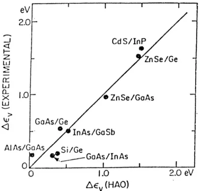
Figure 2.8: Experimental valence band offsets as a function of theoretical valence band offsets calculated by Harrison.
This figure is taken from reference [15]
is obtained directly. Then conduction band discontinuity is determined from the valence band line-up using the values of the band gaps.
Fig. 2.8 and Fig. 2.9 show the comparison of calculated values of band line ups of Harrison with the experimental data. Harrison neglects the electronic dipole shifts due to the charge transfer accross the interface.
Interface Dipoles
To attain a common Fermi level, charge is normally transferred from one sublattice to the adjacent one. The transferred charge creates a dipole field,
Figure 2.9: Experimental valence band offsets of X /G e systems as a function of theoretical valence band offsets calculated by Harrison.
This figure is taken from reference [15]
which in turn affects the natural band line-up.
This effect has been investigated by Tersoff [29]. The interface induces states in the gap of the one or both semiconductors. So the resulting dipole screens the potential step which occurs at the interface. Therefore the band line-up is such that would give zero induced dipole.
In comparison to an effective midgap energy, Eb , the states higher in the gap have more conduction character or lower ones have more valence character on the average. Therefore Eb is something like Fermi level. Alignment of Eb
gives the zero-dipole field band line-up. Eb is the energy where valence and conduction bands contribute equally to the cell-averaged real space Green’s function, G{R^ E), defined by:
G(R, E ) =
I
<PrY:Ji)
= ^ (2.9)Using this formalism Tersoff [30] calculated the valence band discontinuity for II-VI heterojunctions. It is found that the valence band offsets are quite large, 0.5 eV or more, for all telluride pairs, except ZnTe-CdTe, which is the failure of the common anion rule.
Tight Binding Theory of Interface Dipoles
Harrison’s tight-binding approach to the band line-up problem is modified by Harrison and Tersoff [31] such that the interface dipole effect is included. The average sp^ hybrid energy for the semiconductor can be used as an identification.
+ e^)/2 where eh = (e« + 3ep)/4, e, and €p are the atomic s and p eigenvalues, and a and c refer to the anion and the cation, respectively.
The hybrid energies of two semiconductors at the heterojunction differ by A with respect to each other across the interface. The bonds crossing the interface are modified by interface polar energy, Vp = A f 2 and there is a charge transfer ap = ~ i with being the intersite coupling, to the lower energy hybrid. These charges will shift the energy of the hybrids on those atoms and on neighboring atoms so the shift is modified. Therefore a self-consistent scheme comes to use, in order to obtain the final charge distribution and the shift.
Table 2.2: Valence band discontinuities including the dipole effects for selected heterojunctions.
All values in eV. Pinned means dipole field has been taken into account. This table is taken from reference [31]
Heterojunction Experiment Natural Pinned
AlAs/GaAs 0.50 0.03 0.12 InAS/GaSb 0.46 0.72 0.33 GaAs/InAs 0.17 0.16 -0.13 Si/Ge 0.20 0.38 0.29 ZnSe/GaAs 0.96 1.42 1.35 ZnSe/Ge 1.52 2.09 2.01 GaAs/Ge 0.56 0.67 0.66 CdS/InP 1.63 1.86 1.37
Hence the dipole reduces the difference in average hybrids, eh{A) — eh(B), by a factor of Cco- Then the hybrid energy of one semiconductor of the heterojunction lie above the other one by a factor (€k(A) — eh{B))/e^o· Modified valence band discontinuity is
= \eh{A) - e„(A)j - \€h{B ) - e„(H)j
the results of which is shown in Table 2.2.
(
2.
10)
Theories of Self-consistent Interface Potential
Exact potential in the interface determines the electron wave functions so the charge distribution. But the potential is due to the charge distribution. So the electron wave function and the potential are related quantities. They can be obtained self-consistently by taking an approximate trial potential across the interface at the beginning, then an iteration process is initiated. If the
procedure converges, finally, we get the self-consistent potential, wave function and charge distributions.
Final Remarks
Band discontinuity through a heterojunction is an essential property which gives an opportunity to design the energy band diagram for device applications. Because of this, determination of the band line-up is a fundamental problem.
Since the experimental techniques use a model to find out the band line up, accuracy of the measured band line-up value depends on the accuracy of the model. For a given material it is possible to see more than one measured values of band offsets.
There are several approaches to determine the band line-up theoretically. Harrison’s tight-binding theory is a simple theory but gives very reliable results. Although it gives the best results, it is not quite known why it works. Self- consistent potential considers the dipole effects, but they require appreciable amount of computation time.
2.4
Growth
Epitaxy is the growing of the crystalline semiconductor films such that crystallinity and the orientation are determined from the substrate. Heteroepitaxy is named for the growing of different atomic layers on top of each
other. In the past decade, precisely controlled crystal growth techniques such as molecular beam epitaxy (MBE) and metal-organic chemical vapor deposition (M OCVD) have been developed considerably. New possibilities for fabrication of artificially layered semiconductor structures arising from these techniques are the domain of so-called band gap engineering.
There are three methods commonly used in the growth of superlat tices [32]. In liquid-phase epitaxy, the molten metallic solution which contains the components needed to grow the layer is cooled slowly while it is in contact with the substrate. More common technique is the chemical-vapor deposition in which the growth results from the reaction of the substrate with the heated stream of gaseous elements or compounds. When organometallics are used as source then it is called the metal-organic chemical-vapor deposition (MOCVD). At atmospheric pressures, although, one can achieve very high growth rates, at low pressures MOCVD offers atomic layer epitaxy.
Molecular beam epitaxy (MBE) makes possible the preparation of structures with superlattice periodicity ranging from a few tens of nanometer down to the width of a monolayer. In addition, they have highly controlled characteristics such as chemical composition, dopant concentration and profile, as well as thickness uniformity. Under ultra-high vacuum (UHV) conditions, thermal atomic and molecular beams are directed to the heated single crystal substrate. Co-evaporated constituent elements of the epitaxial layer and
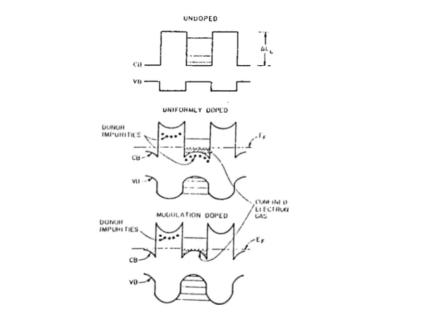
We have also opportunuities in doping. Modulation doping is one way for enhancing mobilities in heterostructures. In this method, barrier regions are doped while the well regions are not. Donors in the barrier layers are ionized and electrons are transferred to the well layers as shown in Fig. 2.11. As a
U N U O P E D Cl) V|j ■f
L
j
:
rUNI KOR ML Y UOPEO
Vfj
Figure 2.11: Energy band diagram for n-doped and undoped superlattices. a) undoped superlattice b) uniformly doped superlattice c) modulation doped
superlattice
result the ion cores and electrons are seperated from each other. Ion cores are scattering centers which increase the resistivity. The mobility increases in this structure because of this seperation. Measured mobilities parallel to the layers are much larger than those of a uniformly doped structures and in bulk spatial
seperation between carriers and scatterers. Band bending seen in Fig. 2.11 has occured because of electron accumulation near the interfaces due to the attraction by the space charge in the barrier regions.
Computer-controlled shuttering of molecular beams gives the ability to gi-ade the composition of compound semiconductors. This gives us an opportunity of fabricating novel devices such as unipolar graded rectifires, grtided and superlattice avalanche photodetectors and lasers, and high-gain hetorojunction bipolar transistors.
As an example, consider the avalanche photodiode [35]. In a photodiode, photo-generated electrons and holes are collected by metallic contacts which passes them to the external circuit as photocurrent. In the case of the avalanche photodiode, high electric field causes the carrier multiplication, so the enhanced photocurrent. The gain and the excess noise factor is strongly dependent on the ratio of the ionization coefficients of electrons and holes, a and ^ respectively. The ionization coefficient is defined as the average number of the secondary pairs created per unit length by impact ionization by an electron or hole along the direction of the electric field. Figure 2.12 shows the energy band diagram of the Alo.45Gao.55As/GaAs superlattice APD
(AEc=0A5
eV, and AF?„=0.08 eV). To show the avalanche multiplication, consider a hot electron accelerating in an AlGaAs barrier layer. When it enters GaAs well, it gains an energy equal to the conduction band discontinuityAEc=0A5
eV. So the ionization energy can beFigure 2.12: Energy band diagram of a staircase avalanche photodiode This figure is taken from Reference [35]
considered as reduced by this amount with respect to the bulk GaAs (Ionization energy E j=2.0 eV). Since the impact-ionization rate a increases exponentially with decreasing E,·, a large increase in the effective a with respect to bulk GaAs is expected. Because the valence band discontinuity of 0.08 eV is much less than AEc, the hole ionization rate ^ is not substantially increased. So we get an enhancement in the | ratio which leads to a low- noise avalanche photodiode.
In this example, ^ = 8 which shows a factor of 4 enhancement over the value in bulk GaAs.
2.6
Resonant Tunneling
Another interesting application of 2D systems is the resonant tunneling. Consider undoped Gax_j;Ala,As-GaAs- Gai_a,AliAs heterostructure as shown in Fig. 2.13. Under a small positive bias applied to the electrode on the right,
o
UJ
DISTANCE
(a)
VOLTAGE(b)Figure 2.13: Resonant tunneling model for heterostructures.
Resonant tunneling model for an undoped GaAlAs-GaAs-GaAlAs heterostructure placed between heavily doped GaAs electrodes.
This figure is taken from referance [36]
the tunneling probability is small, and so is the current between two electrodes. When the bias applied to the structures is such that the energy of the quantum
state Eo is within the Fermi energy of one of the electrodes, resonant tunneling occurs and the tunneling current increases. When Eo falls below the conduction band edge of the electrode the current drops to zero because of conservation of momentum parallel to the interfaces. At very high bias, one of the barriers effectively dissappears and the current increases again [36]. The energies of the bound states can be obtained from such resonant curves: half of the voltages at the current peaks correspond to the bound energies. Possible technological applications of resonant tunneling characteristics are quantum well oscillators at frequencies up to IS GHz, room temperature negative resistance, persistent photocarriers in quantum well resonators, and so on.
2.7
Quantized Hall Effect
A new experiment which is performed by von Klitzing in 1980 about an old known phenomena. Hall effect, brings an insight in physics which is known as quantum Hall effect, integral or fractional [37]. To observe the Hall effect, a planar sample of conductive material is placed in a magnetic field perpendicular to the sample’s surface. Then a small electric current is made to pass from one end to the other, and the voltages and currents through the two direction of the plane were measured.
K. von Klitzing performed the Hall experiment on a silicon field effect transistor in which the electrons are free to carry current are confined within a thin layer. He found that the electrical resistance and the Hall resistance
were dramatically different from the ordinary Hall measurements when the devices are cooled down to within about a degree of absolute zero and placed in extremely strong magnetic fields. As seen in the Figure 2.14 the Hall resistance,
MAGNETIC FIELD B(kG)
Figure 2.14: Hall resistance and electrical resistance of a GaAs/AlGaAs heterojunction.
This figure is taken from reference [32].
instead of increasing steadily and linearly as the strength of the magnetic field is increased, exhibits a series of plateaus. The Hall resistance is quantized to values where v is an integer. In a heterojunction fractional values are also
observed. Electrical resistance drops to zero in the same interval of magnetic field where the Hall resistance exhibits plateaus.
In a two dimensional electron system a magnetic field perpendicular to the ¡^lane of electrical confinement leads to the full quantization of the electron motion. The energy spectrum consists of sharp Landau levels seperated by the cyclotron energy TiUc. A quantized Hall resistance is resulted if the carrier density and the magnetic field are adjusted such that the filling factor v of the energy levels is an integer, since the electrons are moving like free particles.
2.8
Research Areas
Active research areas on two dimensional electron systems can be itemized as follows:
• B an d discon tin u ity: Since the band line-up is the fundemantal property of heterostructures, its determination both experimentally and theoretically is important. Although there are a lot of work about this subject, there is a need for further study. •
• G row th tech n iq u es: In addition to MBE and MOCVD, new techniques such as gas source MBE [38], low pressure MOCVD [39], chemical beam epitaxy (CBE) [40], hot wall epitaxy (HWE) [41], and atomic layer epitaxy (ALE) [42] have been explored for superlattice growth.
• T ra n sp ort p ro p e rtie s: Transport properties of one dimensional and two dimensional systems under electrical and magnetic fields are not known completely yet.
• F raction al qu an tu m H all effect: Although the integer quantized Hall effect was explained in terms of Landau levels, fractional quantum Hall effect has no full explanation.
Chapter 3
Electronic Structure of Strained
S i/G e Superlattices
3.1
strained S i/G e Superlattices
Condensed research on layered structures, i.e. superlattices, results in valuable improvements on device physics. In such structures, to avoid the defects on the interface it is necessary to use materials with similar crystal structures and nearly same interatomic distance. In other words, for defect free growth, matched lattice structures and lattice constants are essential.
Figure 3.1 shows the plot of energy gaps at 4.2K versus lattice constants for zinc-blende semiconductors together with Si and Ge. Joining lines represent ternary alloys. Superlattices and quantum wells or heterojunctions grown with pairs selected from those materials, include InAs/GaSb(/AlSb), InAlAs/InGaAs [43], InP/lattice matched alloys [44,45,46,47], Ge/GaAs [48,49], CdTe/HgTe [50,51,52], PbTe/PbSnTe [53,54], ZnS/ZnSe [41,55], and
ZnSe/ZnTe [56].
Figure 3.1: Energy gaps versus lattice constants at 4.2 K This figure is taken from reference [57]
As seen in Fig. 3.1 , silicon has a small lattice constant (5.43A) which is closely matched by only three other common semiconductors: GaP, AlP, and ZnS. These materials consist of the elements which are effective at generating free carriers in silicon, but germanium is not. Although germanium has the same crystalline structure with silicon , its lattice constant is about %4 larger.
Nowadays, it is possible to grow the dislocation-free, strained-layer super lattices involving thin layers of semiconductors with large lattice mismatch. [58] Fig. 3.2 shows the critical layer thickness for strained-layer epitaxy of GeSi on Si and Ge as a function of alloy composition.
X FOR G6x Si,.x ON Ge 1.0 0.9 0.0 0.7 0.6 0.5 0.4 0.3 0.2 01 0.0
X FOR Gex Sii-x ON Si
Figure 3.2: Critical layer thickness as a function of alloy composition This figure is taken from reference [59]
In the Si/Sii_a;Gea; system grown on the Si(OOl) substrate the lattice mismatch is completely accommodated by the uniform lattice strain in the commensurate Sii_a;Gea; layers. The layers parallel to the interface preserve the registery of the Si substrate, while the lattice constant in the perpendicular direction expands resulting in a tetragonal distortion. Since the energy barrier associated with reordering of atoms is too high, many defect-free commensurate layers can grow before the accumulated strain energy is relaxed by the generation of the misfit dislocations. The number of grown layers decreases with increasing x (or Ge content in the alloy) [60].
The strain is such that the band diagram of these structures is not just perturbed but changes considerably. Working with strain Hamiltonians and deformation potentials gives that the band gaps of GorSii-j; and Si depend strongly on the relative allocation of strain [61]. Fig. 3.3 shows the calculated results for the minimum bad gaps of several materials as a function of the atomic
Figure 3.3: M inimum band gap of Gej;Sii_a; as a function of germanium fraction
This figure is taken from reference [61]
fraction of germanium.
Lastly, it is observed that the two-dimensional electron systems in Si/Sii_iGex strained-layer superlattices with enhanced low-temperature
Recently, the growth of the pure Ge(i.e. x = 1) upto six layers restricted to the Si(OOl) surface unit cell have been achieved [63]. Most importantly novel electronic properties of these strained Sin/Ge„(001) superlattices have been reported [63,64,65,66] offering new device applications.For example, Pearsall et al. [63] observed direct optical transitions at 0.76, 1.25, and 2.51 eV which were found neither in the constituent crystals (i.e. Si and Ge), nor in the Sio.sGeo.s alloy. It is hoped that the well developed Si technology will be used in optoelectronics, especially in laser applications.
This important property, i.e. the lowering of direct gap upon the formation of superlattice and electronic structure is studied by Ciraci and Batra [66,67], and Fi'oyen, Wood and Zunger [68] using self-consistent field pseudopotential. The observed optical transitions were also investigated by using the effective mass approximation [69] and the tight binding method [70].
bilities [62].
3.2
Empirical Tight-binding Method
There are many methods to obtain the band structures of solids in the Energy Band Theory, such as the Augmented Plane Wave Method, the Orthogonalized Plane Wave Method, the Cellular, the Pseudopotential Method, the Tight-binding Method and more accurate methods such as Self-consistent Field calculations or first principal calculations. Linear combinations of atomic
orbitals (LCAO) or tight-binding method (TBM ) is the most simplest one in practice for solving the periodic problems.
TBM has originally been suggested by Bloch and depends on making the linear combination of atomic orbitals located on the various atoms of the crystal with the coefficients as the plane waves exp(ikR) where R is the position vector at which the atom is located [71]. Arising of the difficult integrals is the expense of getting solutions showing all the correct symmetry properties of the energy bands and reaching the solutions for every band at an arbitrary point in the Brillouin zone, whereas applying other methods becomes very difficult except at the certain symmetry points, since these integrals are independent of k. So they are calculated somehow once and are used at an arbitrary ¿-point in the Brillouin zone. Furthermore, Emprical Tight-binding method (ETBM) becomes easier by introducing constants for the integrals, they are chosen by a fitting procedure to the result of more accurate calculations made by other methods at the special symmetry points of Brillouin Zone, or to some experimental data.
Now, let us take an atomic orbital <f>n(r — Ri — ri), located on an atom at vector position Ri -|- ri where Ri is the translation vector and fv is the position vector in the unit cell and n is the principal quantum number. Then foi'm the Bloch sum:
=
/J n R , - n ) (3.1)We can then set up a wave function consisting of a linear combination of all 43
these Bloch sums:
0 (3.2)
n,i
There will be a matrix elements of the hamiltonian between these Bloch sums and these matrix components is made up from the integrals:
J - R , - Ri - f i ) d v (3.3)
which will be replaced by disposable constants resulting from the fitting procedure, where the work on the lattice symmetry and neglecting the far interactions reduces the size of the matrix. Then variational calculus gives us a secular equation:
[H - iE]a = 0 (3.4)
Resulting wave functions and energy levels from this secular equation are the solutions of the periodic potential problem.
3.3
Electronic Structure of Strained Si„/Ge„(001)
Superlattices
3.3.1
Overview
The electronic structure of the strained Sin/Ge„(001) superlattices for n ranging from 1 to 8 is investigated. Results were summarized in the previous publications [72,73]. This paper presents our results providing an understanding of the effect of the superlattice periodicity on the electronic properties. The strained superlattices are constructed by taking Si atoms in their ideal positions,
and by using the lattice constant of Si for the lateral lattice constant of the supercell. The separation of the Si(OOl) and Ge(OOl) layers at the interface, and the interlayer distance in the Ge site are obtained from the self-consistent field (SCF) pseudopotential calculations [64,65,66]. The structural parameters relevant to our study, and the superlattice Brillouin zone (SLBZ) are shown in Fig. 3.4. In the same figure the relation between the symmetry points of the parent crystal BZ and that of the SLBZ, i.e. zone folding for the Sis(OOl) superstructure is also shown.
3.3.2
The M ethod
The purpose of the present work is to reveal how the electronic properties depend on the superlattice periodicity, rather than an accurate calculation of the band gap. Therefore, the electronic band structures are obtained by using the empirical tight binding (ETB) method. In fact an accurate calculation of the band gap by using an SCF-method within the local density functional theory seems to be a distant goal. On the other hand, a great care has to be exercised on the following points to obtain reliable results from the ETB calculations for a system consisting of two different crystals: (i) The set of the energy parameters: We have used the energy parameters which are capable of yielding fairly good conduction bands, and which were proven to be successful in many previous applications [74]. (ii) The effect of the strain on the energy parameters: In the pseudomorphic Si/Ge system the Si-Ge and Ge-Ge interatomic distances, d, deviate from their ideal values because of the strain imposed by the lattice
R·
X
a)
R,
M = X
Figure 3.4: Unit cell and Brillouin Zone of Si„/Ge„(001) superlattices (a) Unit cell of the Si„/Ge„(001) strained superlattice, with dots and dotted circles representing the Si and Ge atoms, respectively. The lateral lattice constants Ri and R2 are 5.43 A/\/5, the perpendicular lattice constant R3 ( / / [001] direction) changes
according to n. Interlayer distances are di=5.43 A/4, ¿2=(5.43+5.65)
A/8
and¿3=5.82 A/4. Lattice constants of bulk Si and Ge are taken to be 5.43
A
and 5.65A ,
respectively.(b) The corresponding Superlattice Brillouin Zone (SLBZ). The width of T-Z decreases with increasing n. (c) The zone folding for the X- and L-points of the fee BZ onto the SLBZ. To avoid the confusion the X and L symmetry points of the feeBZ are shown with bars.
mismatch. This effect is taken into account by the scaling [75,26] of the energy parameters, (iii) The band discontinuity: The energy of the valence band maximum, and also the average value of the crystal potential in two
sublattice crystals (Si and Ge) are different [76]. This is the origin of the natural band lineup. Furthermore, to attain a common Fermi level, charge is normally transferred from one sublattice, to the adjacent one. The transferred charge creates a dipole field, which in turn affects the natural band lineup. While the dipole field induced by the transfer of charge, and thus the band discontinuity at the valence band, AEy, is directly obtainable by the SCF methods, this has to be implemented in the ETB calculations by shifting the self-energies, A E = < <f>i(r) I H I >, of Ge orbitals. We have examined the effect of the band lineup on the direct and indirect band gaps by calculating the electronic structure of Sin/Ge„(001) for A E ranging from —1.0 eV to 1.5 eV.
3.3.3
Calculations
As seen in Fig. 3.5, the ordering of the gaps of Si4/G e4(001) relevant to our study is unaltered for -0 .9 < A E < 0.25 eV. In this energy range the states of Ge at the L-points of the BZ (which is folded near the X-points of the SLBZ) dominate the minimum of the conduction band. However, the ordering changes in the region 0.25 < A E < 1.5 eV several times. Beyond A E > 0.5 eV the minimum occurs at the Z-point. Because of the size effect, and the Si-Ge interaction at the interface, A E is not identical with AE^. In the rest of this study we used the values of A E which incorporates the values calculated by the SCF-pseudopotential method [64,65].
To reveal the effect of the superlattice formation on the electronic 47
AE(eV)
Figure 3.5: Variation of various gaps as a function of A E for the strained Si4/G e4(001) superlattice.
Indices V and c stand for the highest valence band and lowest conduction bands at the
indicated SLBZ points respectively.
structure, we present the bands of Si8(001) superstructure in Fig. 3.6a. The bands of the strained Ge8(001) superstructure ( in which the lateral lattice constants Ri= R2 are taken to be equal to that of the ideal Si, but interlayer distance, ¿3, is expanded to accomodate the lateral strain ) are shown in Fig. 3.6b.
Silicon crystal has six minima along the A-direction of BZ denoted by the A*-states. The resulting experimental band gap is indirect and 1.1 eV. The direct band gap is large, and the energy difference between the direct and
J • · · · :·· ■ ·. ‘ · : '* .··* *··/·* i:.·*
·-.··-r-'·
···· - CB -- /·*••r ’" . I — V B ✓ , · .·**' *** • *· *’ ·. \ • ·· · · *· .* . · ·** ·· * * • · • . ■ - ( a )-Figure 3.6: Energy band structures of Si8(001), Ge8(001) and Si4/G e4(001) structures
(a) Si8(001) superstructure (b) Ge8(001) strained superstructure restricted to Si(OOl) surface unit cell and (c) the Si4/Ge4(001) strained superlattice restricted to Si(OOl)
surface unit cell. {AE = 0.84 eV.)
indirect band gap, Adi, is ~2 eV. Also Ge is an indirect band gap semiconductor, except that the conduction band minima occur at the eight L-points of BZ. By forming a Si4/G e4(001) superlattice the effect of the zone folding [2], the lattice
strain and the band lineup are combined in the electronic structure. Because of the tetragonal supercell of Si8(001) the bands with k j / [001] are folded along the rZ-direction of SLBZ. In addition to four minima (A*) along the FM-direction, the remaining two minima appear near the Z-point. The important effect of the band folding is that A*· is decreased from ~ 2 eV to 0.4 eV. Bands of Ge8(001) experience similar foldings, and thus the minima of the conduction band occur at the X-point of SLBZ. Because of the tetragonal strain the valence bands, which are degenerate at F, are split and the energy of the highest state rises. The calculated value of the band splitting (0.59 eV) is in fair agreement with those calculated by the SCF-pseudopotential method [64,65,67]. The lowest and unfolded conduction band state at F also rises, the net effect of the strain being the increase of the indirect band gap [67].
Upon the formation of the Si4/G e4(001) superlattice the electronic state of the strained Ge-sublattice has to rise relative to that of the Si-sublattice. A state in one sublattice can match to the state in the adjacent one, as long as their momenta and energies are conserved. If their energies are different, the lower energy state is generally confined in its sublattice. The effective masses along the superlattice axis, and the size of the quantum well may influence the confinment. Also, owing to the coupling between the sublattices of the same kind, the bands of the confined states along ¿ / / [001] direction may have a dispersion. The energy band picture of the Si4/G e4(001) superlattice presented in Fig. 3.6c illustrates these effects.


![Figure 2.3: Energy band diagram for an abrupt Ge-GaAs heterojunction This figure is taken from reference [11]](https://thumb-eu.123doks.com/thumbv2/9libnet/5688388.114810/25.959.308.623.484.846/figure-energy-diagram-abrupt-gaas-heterojunction-figure-reference.webp)


![Figure 2 . 12 : Energy band diagram of a staircase avalanche photodiode This figure is taken from Reference [35]](https://thumb-eu.123doks.com/thumbv2/9libnet/5688388.114810/44.959.280.646.167.679/figure-energy-diagram-staircase-avalanche-photodiode-figure-reference.webp)
