Comparison of electron and hole charge-discharge dynamics in germanium
nanocrystal flash memories
Imran B. Akca, Aykutlu Dâna, Atilla Aydinli, and Rasit Turan
Citation: Appl. Phys. Lett. 92, 052103 (2008); doi: 10.1063/1.2835455 View online: http://dx.doi.org/10.1063/1.2835455
View Table of Contents: http://aip.scitation.org/toc/apl/92/5 Published by the American Institute of Physics
Comparison of electron and hole charge-discharge dynamics in germanium
nanocrystal flash memories
Imran B. Akca,a兲 Aykutlu Dâna, and Atilla Aydinli
Department of Physics, Institute of Materials Science and Nanotechnology, Bilkent University, 06800 Ankara, Turkey
Rasit Turan
Department of Physics, Middle East Technical University, 06800 Ankara, Turkey
共Received 10 August 2007; accepted 19 December 2007; published online 4 February 2008兲 Electron and hole charge and discharge dynamics are studied on plasma enhanced chemical vapor deposition grown metal-oxide-silicon germanium nanocrystal flash memory devices. Electron and hole charge and discharge currents are observed to differ significantly and depend on annealing conditions chosen for the formation of nanocrystals. At low annealing temperatures, holes are seen to charge slower but to escape faster than electrons. They discharge slower than electrons when annealing temperatures are raised. The results suggest that discharge currents are dominated by the interface layer acting as a quantum well for holes and by direct tunneling for elec-trons. © 2008 American Institute of Physics. 关DOI:10.1063/1.2835455兴
Nanocrystals共NCs兲 of Silicon 共Si兲 and Germanium 共Ge兲 in silicon based dielectric materials have attracted a lot of attention in recent years for applications in opto- and micro-electronics. NCs can be formed, typically, by ion implanta-tion or plasma enhanced chemical vapor deposiimplanta-tion of semi-conductor rich dielectrics and post annealing. Both Si and Ge NCs are being considered for applications in flash memories and they have been studied extensively.1
In order to study charge and discharge dynamics of car-riers in nanocrystal memories, conventional floating gate models have been applied by De Salvo et al.2and later modi-fied to include the discrete nature of the charges.3It is well known that direct tunneling dominates in thinner oxides whereas thicker oxides require Fowler–Nordheim共FN兲 tun-neling. Results of hydrogen annealing experiments in Si NCs pointed to the role of traps in the NCs during charging and discharging, and modeled by Campera and Iannaccone4 Charge retention at deep traps in Ge NCs was also observed.5,6 Seemingly long retention times suggested that carrier discharge occurs through direct tunneling in the ab-sence of interface states.7 However, long retention times are meaningful only when write times are short. Truly long hole retention times were found in chemical vapor deposi-tion 共CVD兲 grown Ge NCs with Si precursors without postannealing.8Theoretically, Ge NCs are thought to be bet-ter suited for data retention due to its smaller band gap com-pared to Si. Recently, it was also suggested9that hole storage in SiGe NCs has important advantages in terms of retention of carriers. However, none of these studies considered the role of interface layers, which should be included in any realistic model of NC memory devices.
In Ge NC formation processes where post annealing is required, typical temperatures used range from 600 to 800 ° C for the formation of Ge NCs. Since Ge is a fast diffuser in SiO2, formation of Ge NCs is often accom-panied by diffusion of Ge into the SiO2/Si interface even at
relatively low temperatures. Considering that the tunnel bar-rier in a flash memory is only a few nanometers thick, it is
hard to avoid diffusion of Ge under these conditions. The presence of Ge at the interface creates an interface layer, which has to be taken into account in any analysis of flash memories. In this work, we present experimental results that compare charging and discharging dynamics of electrons and holes in Ge NC metal-oxide-semiconductor 共MOS兲 capaci-tors fabricated by plasma enhanced CVD 共PECVD兲 with postannealing and discuss the validity of assumptions about dominant carrier discharge mechanisms. Trilayer MOS ca-pacitor structures carrying Ge NCs as charge storage medium has been studied by capacitance-voltage共CV兲 spectroscopy. Electron and hole storage and escape have been character-ized experimentally. The results point to the importance of the interface layer due to Ge diffusion to the SiO2/Si
inter-face.
The samples were grown using a parallel-plate-type PECVD reactor 共PLASMALAB 8510 ° C兲. Germanosilicate
films were grown at 350 ° C, in a pressure of 1 Torr and rf power of 10 W at a frequency of 13.56 MHz, applied to plates with a diameter of 24 cm using GeH4as the precursor.
Trilayer structures consist of a 4 nm thick thermal oxide fol-lowed by a 10 nm thick Si0.6Ge0.4O2layer关as determined by
x-ray photoelectron spectroscopy 共XPS兲 characterization兴, capped with a 15 nm thick PECVD oxide. Annealing was done at temperatures of 650– 850 ° C for duration of 5 min under nitrogen environment. The samples were studied by cross sectional transmission electron microscopy共TEM兲 共not shown兲 and nanocrystal size distributions and areal densities were inferred. It is also observed that, for the fixed duration of annealing, samples annealed at 850 ° C show precipitation of Ge to the silicon substrate interface as discussed elsewhere.10 The charge and discharge currents of NCs can be calculated separately assuming FN tunneling from the substrate to the NC layer during charging and direct tunnel-ing durtunnel-ing discharge.11Diffusion of Ge toward the interface, however, complicates the situation. The possibility of thin homogeneous and inhomogenous alloy layers forming at the interface may lead to trapping and/or trap assisted tunneling which is especially important during retention. Since charge and discharge currents are dependent on a large number of
a兲Electronic mail: [email protected].
APPLIED PHYSICS LETTERS 92, 052103共2008兲
parameters, it is hard to distinguish unambiguously these multiple mechanisms from the measurement and analysis of only the discharge current and single carrier type. However, comparison of charge and discharge currents for electrons and holes provides a greater contrast if the dominant dis-charging mechanism is not direct tunneling. One would ex-pect to observe increased discharge rates if trap assisted tun-neling during discharge is dominant. On the other hand formation of alloy islands or quantum wells at the interface may also inhibit discharge. In order to measure charge and discharge currents, we use a modified CV spectroscopy setup, where a feedback loop is used to measure flatband voltage shifts before and after applied pulses or during reten-tion. The cumulative flatband shift is proportional to the total deposited charge after a number of write pulses and is given by12 ⌬VFB= qnnc 苸ox
冉
tcox+ 苸oxtnc 2苸Ge冊
, 共1兲where q is the electronic charge, tcox is the control oxide
thickness, tncis the average diameter of the NCs, and⑀’s are
the dielectric constants of respective materials. The charging current is assumed to be due to FN tunneling. The charging current density then becomes13
Jc= AFtox2 VB ⫻ exp
冉
−BVB 3/2 Ftox冊
, 共2兲where A = q2mSi/162moxប, B=2
冑
8moxq/3ប, Ftoxis thetun-nel oxide field during charging, mox is the tunnel effective
mass, and VB is the barrier height between the oxide and the
substrate. The differential charges deposited per unit area
d in a time interval d can be calculated through
d= pcDtJc共Ftox兲d, where pc is the average capture cross
section and Dt is the available density of final states. The
capture probability may depend on NC shape and Dt⬇NNC
is the NC areal density. Similar studies of charge and dis-charge current have been recently reported.14 It is well known that, as the storage layer is saturated with carriers, the flatband shift reaches a maximum value in both conventional and NC flash memories.14We, therefore, consider only small flatband voltage shifts for comparison of charge and dis-charge dynamics.
The flatband voltage shift measured between repetitive
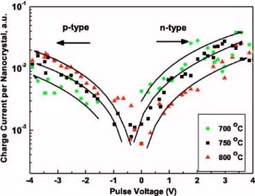
d= 25 ms write pulses of varying voltage values are recorded.11Noting that, the derivative of the flatband voltage shift divided by pulse duration gives the charge current den-sity, we plot the charging current per nanocrystal in Fig.1. It is seen that, for small charging currents, charging current increases monotonically for n and p type samples, in a man-ner proportional to the NC density, consistent with TEM data indicating average diameters of⬃3.1 and ⬃7.4 nm and den-sities of 3.8⫻1012and 8.0⫻1011cm−2for samples annealed
at 700 and 800 ° C, respectively. It is observed that, for volt-age pulse amplitudes of less than 4 V, the charge currents for electron and holes are roughly on the same order of magni-tude, electrons tunneling faster by less than a factor of three than holes. This is understood by noting that hole barrier is greater when SiO2 is used as the tunnel dielectric. The
dis-charge currents have been measured in the same setup by monitoring the flatband voltage shift as a function of time. The derivative of the flatband voltage shift is calculated nu-merically and plotted as a function of time in Fig. 2. The
flatband voltage shifts are with respect to the uncharged de-vices, therefore, the flatband shift due to surface pinning modification is already taken into account. It is seen that, the discharge currents of holes are larger than that of electrons for a similar flatband voltage shift at low annealing tempera-tures. However, as the annealing temperature is raised, hole escape rates drop below those of the electrons, the difference becoming larger at higher the annealing temperatures.
As the direct tunneling current is normally expected to be weak, surprisingly high hole discharge current at low an-nealing temperatures suggests that hole discharge dynamics are dominated by other mechanisms than direct tunneling such as trap assisted tunneling. On the other hand, samples annealed at higher temperatures show very low escape times for holes. This suggests that there is significant trapping of holes during the discharge phase. This could be understood by considering two factors that come into play at higher annealing temperatures. First, as the temperature is raised, nanocrystal sizes increase which in turn results in a higher energy barrier for holes bound at quantum states of the
nano-FIG. 1.共Color online兲 Experimental data of charging of n 共right兲 and p 共left兲 type capacitors. Charging currents as a function of charge voltage are mea-sured for samples annealed at 700– 800 ° C.
FIG. 2.共Color online兲 Discharge current densities as a function of time for
n and p type devices. The holes decay faster than the electrons for samples
annealed at low temperatures whereas they decay much slower for samples annealed at higher temperatures.
crystal. Second, the diffusion of Ge to the interface should result SiGe alloy formation which constitutes a quantum well. This results in more homogenous layer with less inter-face states. In addition, on their way to the substrate, holes encounter to the substrate encounter the quantum well and are trapped at the bound states of the quantum well. In-creased annealing temperatures result in longer diffusion lengths for Ge, hence, wider quantum wells and larger bar-riers for holes trapped in the quantum well.
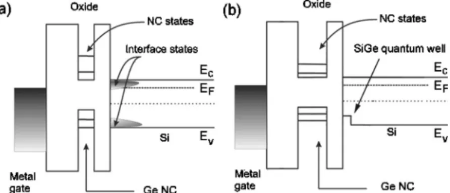
The results are summarized in the schematic band dia-gram for electrons and holes in Fig. 3. Note that at low annealing temperatures, Ge atoms diffusing to the interface do not form a homogenous layer. However, they create sig-nificant amount of interface trap states in the band gap of Si near the valence band edge lie energetically close to the con-fined states of holes in Ge NCs in contrast with electron confined states, which are above the conduction band edge. It can be argued that, both the valance band states and the presence of large number of traps within the silicon band gap result in an increased discharge current, mainly due to trap assisted tunneling of holes,关Fig.3共a兲兴. As the annealing tem-perature is raised, the energy band diagram is modified by the presence of a thin quantum well at the oxide Si interface and the presence of larger nanocrystal sizes, 关Fig. 3共b兲兴. It
should be noted that, introduction of Ge into Si does not change the conduction band appreciably while the valence band is raised.15This is the reason for the different behavior of holes than electrons.
In conclusion, we have studied charge and discharge dy-namics of both electrons and holes in PECVD grown and post annealed Ge NCs MOS capacitors. We find that in con-trast with idealistic models of such devices, hole retention times are actually shorter than electron retention times for samples annealed at low temperatures. We suggest that the observed reduction of hole retention times is due to interface
traps states. However, formation of a Ge rich alloy at the interface with high temperature annealing results in longer retention times, which is promising for actual device opera-tions. These observations emphasize the importance of proper interface engineering for Ge NCs memory devices.
This work was supported by a grant from TUBITAK 共104T115兲 and by European Commission’s FP6 project SEMINANO, under Contract No. NMP4-CT-2004-505285. We are grateful to T. G. Finstad for TEM data and S. Suzer for XPS measurements.
1J. De Blauwe, IEEE Trans. Nanotechnol. 1, 72共2002兲.
2B. De Salvo, G. Gibaudo, G. Pananakakis, P. Masson, T. Baron, N. Buffet, A. Fernandes, and B. Guillaumot, IEEE Trans. Electron Devices 48, 1789 共2001兲.
3C. Busseret, S. Ferraton, L. Montes, and J. Zimmermann, IEEE Trans. Electron Devices 53, 14共2006兲.
4A. Campera and G. Iannaccone, Solid-State Electron. 49, 1745共2005兲. 5M. Yang, T. P. Chen, J. I. Wong, C. Y. Ng, Y. Liu, L. Ding, S. Fung, A. D.
Trigg, C. H. Tung, and C. M. Li, J. Appl. Phys. 101, 124313共2007兲. 6M. She and T.-J. King, IEEE Trans. Electron Devices 50, 1934共2003兲. 7B. H. Koh, E. W. H. Kan, W. K. Chim, W. K. Choi, D. A. Antoniadis, and
E. A. Fitzgerald, J. Appl. Phys. 97, 124305共2005兲.
8M. Kanoun, C. Busseret, A. Poncet, A. Souifi, T. Baron, and E. Gautier, Solid-State Electron. 7-8, 1310共2006兲.
9J. S. de Sousa, V. N. Freire, and J.-P. Leburton, Appl. Phys. Lett. 90, 223504共2007兲.
10S. Foss, T. G. Finstad, A. Dana, and A. Aydinli, Thin Solid Films 515, 6381共2007兲.
11A. Dana, I. Akca, O. Ergun, A. Aydınlı, R. Turan, and T. G. Finstad, Physica E共Amsterdam兲 38, 94 共2007兲.
12R. Scholz, V. Talelaev, and M. Zacharias, Appl. Phys. Lett. 87, 202110 共2005兲.
13M. Lenzlinger and E. H. Snow, J. Appl. Phys. 40, 278共1969兲. 14V. Beyer, J. von Barony, and M. Klimenkov, Appl. Phys. Lett. 89, 193505
共2006兲.
15R. Turan and T. G. Finstad, Semicond. Sci. Technol. 7, 75共1992兲. FIG. 3. Band structure of Ge nanocrystal MOS capaci-tor,共a兲 annealed at low temperatures and 共b兲 annealed at high temperatures. Note the effect of quantum well at the interface and the increased nanocrystal size.