Blue quantum electroabsorption modulators based on reversed quantum
confined Stark effect with blueshift
Emre Sari, Sedat Nizamoglu, Tuncay Ozel, and Hilmi Volkan Demira兲
Deparment of Physics, Bilkent University, Bilkent, Ankara 06800, Turkey; Department of Electrical and Electronics Engineering, Bilkent University, Bilkent, Ankara 06800, Turkey; and Nanotechnology Research Center, Bilkent University, Bilkent, Ankara 06800 Turkey
共Received 18 October 2006; accepted 22 November 2006; published online 2 January 2007兲 The authors present the design, growth, fabrication, experimental characterization, and theoretical analysis of blue quantum electroabsorption modulators that incorporate ⬃5 nm thick In0.35Ga0.65N / GaN quantum structures for operation between 420 and 430 nm. Growing on polar c
plane on sapphire, they obtain quantum structures with zigzag potential profile due to alternating polarization fields and demonstrate that their optical absorption blueshifts with applied electric field, unlike the redshift of conventional quantum confined Stark effect. In InGaN / GaN quantum structures, they report the largest absorption change of 6000 cm−1 for 6 V bias swing around 424 nm, holding promise for blue optical clock generation and injection directly into silicon chips. © 2007 American Institute of Physics.关DOI:10.1063/1.2424642兴
Today silicon microelectronics is limited in operating speed: the electrical interconnects suffer from the RC limita-tion; scaling does not mitigate this problem.1This leads to a bottleneck in electrical clocking. Optical clocking is pro-posed as a remedy.2 Optical clock distribution is imple-mented commonly in the near infrared共IR兲 spectral region where optoelecronic devices are readily available.3,4 How-ever, silicon photodetectors, for example, those fabricated in standard complementary metal-oxide-semiconductor 共CMOS兲 process, unfavorably exhibit long absorption length and thus a diffusion tail problem in the near IR. This limits the operating speed of Si CMOS photodetectors to 1 Gbits/ s.5To circumvent this problem, one approach is to utilize high-speed III-V photodetectors hybrid integrated on Si chips. This, however, introduces difficulties related to post-CMOS fabrication. On the other hand, unlike in the IR, optical clock injection directly to Si is possible in the blue, where Si features a very short absorption length共⬃100 nm at 400 nm兲 and thus lacks the diffusion tail.6
However, there exists no chip-scale device to modulate optical clock signal in the blue at high speeds to date. In this letter, we propose blue InGaN / GaN based quantum electroabsorption modula-tors for a possible chip-scale solution in optical clock modu-lation in the blue. Here we present the design, epitaxial growth, fabrication, experimental characterization, and theo-retical analysis of our quantum electroabsorption modulators that incorporate ⬃5 nm thick In0.35Ga0.65N / GaN quantum
structures in a p-i-n diode architecture for operation in the blue spectral range, as shown in Fig.1.
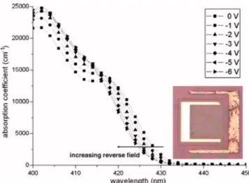
We grow these quantum structures on the polar c plane of GaN on sapphire in metal organic chemical vapor deposi-tion共MOCVD兲 and obtain a zigzag potential profile due to high polarization fields with alternating directions in their heterostructures. We study the electroabsorption behavior of these quantum zigzag structures for proof-of-concept demon-stration of their use in blue modulation. In the blue range, using InGaN / GaN quantum structures, we experimentally demonstrate the largest optical absorption change of 6000 cm−1 with the application of a reverse bias of −6 V
across our diodes共corresponding to 50 cm−1/ 1 V /m field
swing兲 at 424 nm in the highly transmissive region below the band edge. This implies that a modulation contrast ratio of ⬎10 dB is possible with an optical interaction length⬃100m and a field swing of 2 V /m in principle. Opposite to the typical redshift of the traditional quantum confined Stark effect共QCSE兲, we demonstrate in these zig-zag structures that the band edge shifts to shorter wave-lengths共blueshifts兲 with the increasing applied reverse field, as plotted in Fig.1. Our theoretical analysis shows that this reversed behavior of the quantum confined Stark effect stems from high alternating polarization fields.
The conventional quantum structures in nonpolar III-V semiconductors form a steplike potential profile. In such square quantum well structures, we observe quantum con-fined Stark effect,7which brings the electron and hole energy states closer in energy when an external electric field is ap-plied 共in either direction兲. Thus, the traditional QCSE red-shifts the optical absorption edge with respect to the no-field case共where the energy bands are flat兲. However, III-N based quantum structures form a zigzag potential profile due to the
a兲FAX:关⫹90兴共312兲290-1015; electronic mail: [email protected]
FIG. 1. 共Color online兲 Optical absorption spectra measured from our InGaN / GaN based quantum electroabsorption modulator parametrized with the applied reverse bias at room temperature, along with a top-view micro-graph of one of our fabricated devices.
APPLIED PHYSICS LETTERS 90, 011101共2007兲
0003-6951/2007/90共1兲/011101/3/$23.00 90, 011101-1 © 2007 American Institute of Physics
high alternating polarization fields.8 For such quantum zig-zag structures, our quantum mechanical simulations based on transfer matrix method demonstrate that the band edge blue-shifts as presented in Fig.2, verifying our experimental ob-servation in Fig.1, when an external electric field is applied in the opposite direction of the polarization field seen in the wells. Comparing Fig.2共a兲for the zero-field case共F=0兲 and Fig.2共b兲 for the non-zero-field case 共F⫽0 in the opposite direction of the well polarization兲, we observe that E1⬎E0
and thus 1⬍0, where E0,1 are the energy separations be-tween the first electron and hole states and0,1are the
cor-responding absorption band edges in the respective 共a兲 F = 0 and 共b兲 F⫽0 cases. Here we understand that this re-versed QCSE arises because the electric field applied in the opposite direction of the well polarization compensates for the polarization and brings the quantum zigzag structure closer to the flat energy band condition in the wells. On the other hand, when the external field is applied in the direction of the well polarization field, we observe the typical QCSE with a redshift, rather than the reversed QCSE with a blueshift.
The epitaxial design of our modulators is based on a
p-i-n structure that houses InGaN / GaN quantum structures
in its intrinsic region. We grow our epitaxial wafers on
c-plane double side polished sapphire substrates using our
AIXTRON RF200/4 RF-S MOCVD system located at Bil-kent University Nanotechnology Research Center. Our epi-taxial growth starts with a 14 nm thick low-temperautre GaN nucleation layer and a 200 nm thick high-temperature GaN buffer layer for a high crystal quality and then follows a 690 nm thick Si doped GaN layer for n-type contact. Subsequently we grow our active region that consists of five ⬃5 nm thick In0.35Ga0.65N well and ⬃5 nm thick GaN
barrier structures at a constant temperature of 682 ° C. We finalize our growth with Mg doped, 50 nm thick Al0.1Ga0.9N
and 120 nm thick GaN layers—both p type, with the latter serving as the p-contact layer. In our MOCVD epigrowth, we use TEGa共for quantum structures兲, TMGa 共for bulk layers兲, TMIn, TMAl, and NH3as the precursors.
We start the device fabrication with the dehydrogenation of Mg dopants by annealing our epitaxial wafers at 750 ° C for 15 min in N2 ambient atmosphere. We use standard
li-thography for reactive ion etching of device mesas and sub-sequent metallization steps. We evaporate Ni:Au and Ti:Al layers共both 10/100 nm thick兲 for p and n contacts,
respec-tively. We finally apply rapid thermal annealing at 650 ° C for 1 min. Our fabricated devices have mesa sizes varying from 10⫻10 to 300⫻300m2, with open optical windows
to couple light into and out of the mesa in surface-normal operation.
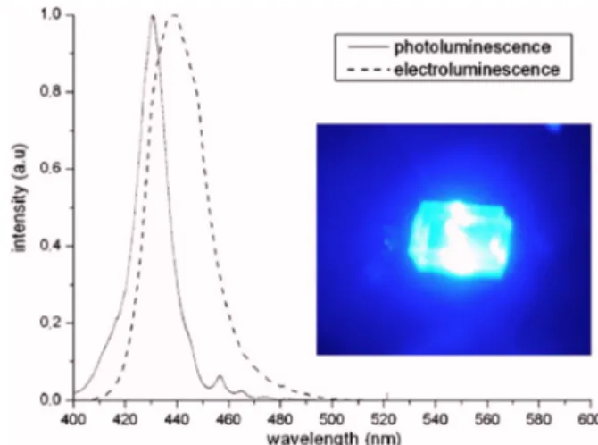
We perform photoluminescence共PL兲 characterization at room temperature using a He–Cd laser at an excitation wave-length of 325 nm. We observe the PL peak at 430 nm with a full width at half maximum共FWHM兲 of 14 nm, as shown in Fig. 3. This verifies the proper epigrowth of ⬃5 nm thick In0.35Ga0.65N / GaN quantum structures. In forward bias,
these InGaN / GaN devices exhibit strong electrolumines-cence共EL兲. Figure 2also shows the EL spectrum when the diode is driven with 10 mA of current, along with a micro-graph of the blue light emitted from the device. The optical power coupled from one side is⬎0.35 mW at a current in-jection level of 20 mA. EL spectrum peaks at 437 nm 共red-shifted with respect to PL兲 with a FWHM of 25 nm.
We measure the optical absorption spectra using our photocurrent measurement setup including a monochro-mator, a xenon lamp, a lock-in amplifier, a power meter, and a dc power supply for the application of various reverse bias voltages. Figure1shows the optical absorption spectra from 400 to 460 nm parametrized with the applied reverse biases from 0 to − 6 V共with the dark current levels in the range of few nanoamperes兲. Here we observe that the optical absorp-tion edge blueshifts with the increasing applied reverse field, unlike in the case of the conventional QCSE. This blueshift is a direct experimental evidence of the polarization fields seen in the wells in the opposite direction of the applied reverse field 共thus, in the opposite direction of the built-in field兲. Therefore, the well polarization field lies in the oppo-site direction of the epi-growth and extends from the top epitaxial layer共p side兲 toward the bottom epitaxial layer 共n side兲, verifying the expected direction of the polarization in the InGaN wells on polar c plane.9Also, in Fig. 1, we ob-serve an inflection point at 418 nm on the absorption curves of our InGaN / GaN quantum structures under different bi-ases, which is in agreement with the work of Friel et al. on GaN / AlGaN quantum structures.10 For reverse biases close to −6 V and beyond, the barriers that have polarization in the same direction as the applied reverse field turn into consid-erably thin potential barriers, exhibiting transition from the quantum confined case to the bulk case, also observed in Fig.
FIG. 2. Electron and hole energy states共a兲 for the nonbiased case 共F=0兲 and共b兲 for the biased case 共F⫽0兲, simulated by the transfer matrix method. Here E1⬎E0, which implies1⬍0for the corresponding absorption band edges.
FIG. 3.共Color online兲 Photoluminesence and electroluminesence spectra of our InGaN / GaN based quantum electroabsorption modulator, along with a micrograph of the emitted blue light when the diode is forward biased.
011101-2 Sari et al. Appl. Phys. Lett. 90, 011101共2007兲
1. From the compensation of the polarization field with the applied field, we experimentally predict the intrinsic polar-ization field in the wells to be 120 V /m, which is compa-rable to the theoretically expected 300 V /m.
Figure 4 shows the optical absorption spectrum of our InGaN / GaN quantum zigzag structures when a forward bias of 1 V is applied, along with the spectra under a reverse bias of −1 V and no bias for comparison. Here we observe that the absorption spectra differ for different directions of bias application 共despite comparable levels of leakage current兲. The absorption spectrum appears more to redshift due to the traditional QCSE when forward biased共i.e., when the elec-tric field F is applied in the direction of the well polarization
P兲 and to blueshift due to the reversed QCSE when reverse
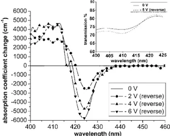
biased共i.e., when F is applied in the opposite direction of P兲. Figure5 shows the electroabsorption coefficient change 共with respect to the no-bias case兲 with the largest change of 6000 cm−1 for a 6 V swing 共corresponding to 50 cm−1
ab-sorption coefficient change for 1 V /m field change兲 at 424 nm. Here the blue region between 420 and 430 nm is a very good operating wavelength range for such a modulator with large absorption change and low background absorption 共as low as 767 cm−1兲. In Fig. 5, we also show the optical
transmission spectra modulated with the reverse bias in the inset. The transmission and absorption spectra lead to the same observations of the blueshift and inflection point at 418 nm. Here, in the surface-normal configuration, the short optical interaction length of 50 nm 共along with 17% stray light not passing through the mesa兲 renders a low transmis-sion modulation of 3.05% at 424 nm for 5 V bias, as also expected by the absorption spectra.
For electroabsorption, we observe a maximum optical absorption change of 67 cm−1/ 1 V /m field swing between the reserve biases 0 and −2 V. This electroabsorption effect is stronger than those previously observed in bulk GaN based materials11 and in InGaN / GaN quantum structures of blue laser diodes.12 This implies that a 100 m long waveguide modulator with a reasonable overlap integral of the wave-guide mode with our InGaN / GaN structures共e.g., ⌫⬃0.1兲 is expected to achieve a 10 dB contrast ratio for a 2 V /m field swing. This further means that the electroabsorption performance of these InGaN / GaN quantum zigzag structures in the blue is comparable to that of the InGaAsP / InP quan-tum well structures in the near IR 共e.g., c band兲,13,14 also commercially used in communications. Furthermore,
be-cause of the low parasitic in-series resistance共⬍100 ⍀兲 and low capacitance共⬍100 fF for a 3⫻100m2 lateral device
area兲, blue InGaN/GaN quantum electroabsorption modula-tors hold promise for⬎10 GHz optical clock generation and injection directly into Si CMOS chips in the blue. Addition-ally, the electroluminescence of these InGaN / GaN quantum devices in the blue range makes it possible to consider on-chip integration of blue light source and modulator for a compact optical clocking scheme.
In conclusion, we presented blue InGaN / GaN based quantum electroabsorption modulators that find application in blue optical clock injection directly into Si CMOS, unlike in the infrared. Using our InGaN / GaN quantum zigzag structures, we demonstrated strong electroabsorption behav-ior with a blueshift due to the reversed quantum confined Stark effect.
This work is supported by EU MOON 021391, EU NOE PHOREMOST 511616, Turkish Academy of Sciences TUBA GEBIP, and TUBITAK EEEAG 104E114, 106E020, 105E065, and 105E066.
1D. A. B. Miller and H. M. Özaktas, ARTE CEMENTO 41, 42共1997兲. 2J. W. Goodman, F. I. Leonberger, and S. Y. Kung, Proc. IEEE 72, 850
共1984兲.
3D. A. B. Miller, Int. J. Eng. Sci. 11, 155共1997兲.
4G. Li, D. Huang, E. Yuceturk, P. J. Marchand, S. C. Esener, V. H. Ozguz,
and Y. Liu, Appl. Opt. 41, 348共2002兲.
5T. K. Woodward and A. V. Krishnamoorthy, Electron. Lett. 34, 1252
共1998兲.
6A. Bhatnagar, S. Latif, C. Debaes, and D. A. B. Miller, J. Lightwave
Technol. 22, 2213共2004兲.
7D. A. B. Miller, D. S. Chemla, T. C. Damen, A. C. Gossard, W.
Wiegmann, T. H. Wood, and C. A. Burrus, Phys. Rev. B 32, 1043共1985兲.
8V. Fiorentini, F. Bernardini, F. D. Sala, A. Di Carlo, and P. Lugli, Phys.
Rev. B 60, 8849共1999兲.
9T. Takeuchi, C. Wetzel, S. Yamaguchi, H. Sakai, H. Amano, I. Akasaki, Y.
Kaneko, S. Nakagawa, Y. Yamaoka, and N. Yamada, Appl. Phys. Lett. 73, 1691共1998兲.
10I. Friel, C. Thomidis, and T. D. Moustakas, J. Appl. Phys. 97, 123515
共2005兲.
11A. E. Oberhofer, J. F. Muth, M. A. L. Johnson, Z. Y. Chen, and E. F. Fleet,
Appl. Phys. Lett. 83, 2748共2003兲.
12M. Kneissl, T. L. Paoli, P. Kiesel, D. W. Treat, M. Teepe, N. Miyashita,
and N. M. Johnson, Appl. Phys. Lett. 80, 3283共2002兲.
13N. C. Helman, J. E. Roth, D. P. Bour, H. Altug, and D. A. B. Miller, IEEE
J. Sel. Top. Quantum Electron. 11, 338共2005兲.
14H. V. Demir, V. A. Sabnis, O. Fidaner, J. S. Harris, Jr., D. A. B. Miller,
and J.-F. Zheng, IEEE J. Quantum Electron. 11, 86共2005兲. FIG. 4. Optical absorption curves measured under 1 V共forward bias兲, 0 V
共no bias兲, and −1 V 共reverse bias兲 at room temperature.
FIG. 5. Optical absorption coefficient change with respect to 0 V, along with transmission spectra at 0 and −5 V in the inset.
011101-3 Sari et al. Appl. Phys. Lett. 90, 011101共2007兲