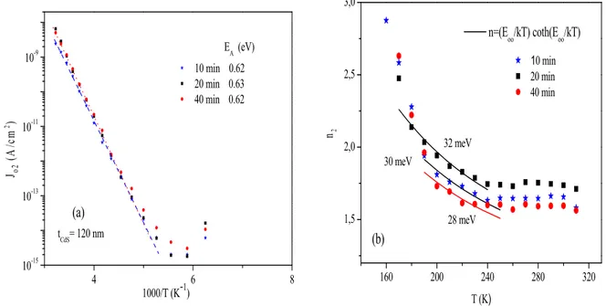
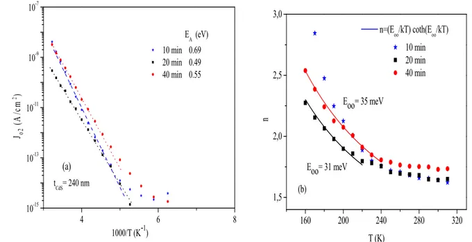
Regimes of current transport mechanisms in CdS/CdTe solar cells
Tam metin
Şekil


Benzer Belgeler
In the second chapter we have started with Schwarzschild spacetime equation and we assumed that each planet moves as a test particle for the motion of the planets in
Limitations: The primary limitation in the simulations per- formed is the simulation of a cell with lesser absorber thickness (100 µm) instead of the dimension of the
Peter Ackroyd starts the novel first with an encyclopaedic biography of Thomas Chatterton and the reader is informed about the short life of the poet and the
Bu çalışmada, semi pozitif ortogonal dönme matrisinin bulunmasında alternatif diye adlandırılan iki farklı metot veriliyor. Ayrıca, semi-pozitif ortogonal A matrisine karşılık
• The change of an electric current or the amount of reduced and oxidized matter in the interfaces is directly proportional to the amount of electricity passing through the
47 Otomatik Kontrol (Transfer Fonksiyonlar ) - Ders sorumlusu: Yrd.Doç.Dr.Hilmi Ku çu... 48 Fizik I (Tek ve ki Boyutta Hareket) - Ders sorumlusu: Yrd.Doç.Dr.Hilmi
• Operating cycle = inventory period + accounts receivable
5 Otomatik Kontrol (Transfer Fonksiyonlar ) - Ders sorumlusu: Yrd.Doç.Dr.Hilmi Ku çu... 7 Otomatik Kontrol (Transfer Fonksiyonlar ) - Ders sorumlusu: Yrd.Doç.Dr.Hilmi
