https://doi.org/10.1007/s10854-020-02944-4
The effects of air, oxygen and water exposure on the sub‑bandgap
absorption, the electronic conductivity and the ambipolar
diffusion length in highly crystalline microcrystalline silicon films
for photovoltaic applications
Mehmet Güneş1 · V. Smirnov2 · F. Finger2 · R. Brüggemann3
Received: 7 November 2019 / Accepted: 20 January 2020 / Published online: 1 February 2020 © Springer Science+Business Media, LLC, part of Springer Nature 2020
Abstract
Reversible and irreversible changes due to long term air and short term de-ionized water (DIW) or pure oxygen exposure were investigated in about 1 µm thick hydrogenated microcrystalline silicon (µc-Si:H) films deposited on rough glass sub-strates, thereby comparing highly crystalline with compact material. Time and temperature dependent dark conductivity, steady-state photoconductivity, the steady-state photocarrier grating and dual-beam photoconductivity methods have been used to study the effects. Standard measurement procedures defined previously have been carefully applied to record the changes after different treatments using the steady-state methods under light. After long term air exposure of highly crystal-line µc-Si:H films, a thermal annealing step leads to an increase in dark conductivity (σD) and steady-state photoconductivity
(σph) as well as to a significant increase in the sub-bandgap absorption. These effects are likely due to a reversible recovery from surface adsorbents in a porous microstructure after air exposure resulting in surface charge and Fermi level shifts in agreement with earlier results. Compact µc-Si:H films showed only marginal effects upon an annealing after long term air exposure suggesting much reduced susceptibility to surface adsorbent induced by Fermi level shifts. Five hours exposure to de-ionized water at 80 °C caused more than an order of magnitude increase in σD and σph and a substantial decrease in the sub-bandgap absorption spectrum in highly crystalline as well as in compact µc-Si:H films. In addition, minority car-rier diffusion lengths measured by the steady-state photocarminority car-rier grating method improved significantly. The changes after exposure to water were not reversible upon our standard annealing procedure. Exposure to high purity oxygen gas at 150 °C resulted in similar effects like the exposure to DIW. Also here the changes in material properties were not reversible upon annealing. Results are discussed in terms of adsorption and chemical reactions on surfaces in the porous highly crystalline material versus the materials with more compact structures. Results are compared to earlier observations and consequences for device application will be indicated.
1 Introduction
Hydrogenated microcrystalline silicon (µc-Si:H) has been investigated over the last three decades and applied suc-cessfully in photovoltaics and microelectronics (e.g. thin film transistor devices) [1–3]. While in the past photo-voltaic applications of µc-Si:H were mainly for thin film silicon based solar cells [4], recently µc-Si:H and related alloys are also of considerable interest for Si wafer based heterojunction solar cells [5–7]. For these device applica-tions long-term electronic and mechanical stability is of high importance and observations that µc-Si:H can show strong instability or metastability effects upon storage at ambient with exposure to atmospheric gases are of concern * Mehmet Güneş [email protected] V. Smirnov [email protected] F. Finger [email protected] R. Brüggemann [email protected]
1 Department of Physics, Mugla Sitki Kocman University,
Kötekli Yerleskesi, Mugla 48000, Turkey
2 Forschungszentrum Jülich, IEK-5 Photovoltaik, Jülich 52425,
Germany
3 Institut für Physik, Carl Von Ossietzky Universität
and several reports on a number of phenomena have been published already starting with the first communications on µc-Si:H [8].
Microcrystalline silicon (also known as nanocrystalline silicon) is a wide range of mixed phase material consisting of an amorphous silicon phase or better disordered phase, a micro (-nano) crystalline phase and voids. The structural composition can be adjusted during the deposition process and the range of possible nanostructures seems to be inde-pendent of the deposition method used. Electronic defects mainly exist in the disordered regions between crystalline grains, along the grain boundaries and on the surface of such grains (for a summary see Shah [4]). Hydrogenated micro-crystalline layers which are prepared using decomposition of pure silane diluted strongly in hydrogen with “plasma enhanced” or “hot wire” chemical vapor deposition (PECVD or HWCVD) can have a wide range of dark conductivities over several orders of magnitude even without adding any intentional doping. Suggested reasons for this are variations in the structure compositions, doping effects of build-in impurities such as oxygen or nitrogen [9, 10] surface charge on inner and outer surfaces induced by adsorption and oxida-tion or a combinaoxida-tions of these effects. Reliable determina-tion of the type of majority carrier (n- or p-type) in undoped µc-Si:H material by Hall effect or thermo power measure-ments is not available; however, it is plausible to assume and it is in agreement with numerous experimental observations that such material is usually n-type and the described vari-ation in the dark conductivity can be related to Fermi level shifts in the upper half of the band gap. We will assume the same interpretation for our experiments described in the present study.
Metastability and instability effects in undoped µc-Si:H such as variation of their electrical properties upon exposure to ambient atmosphere or alternatively to pure oxygen or water have been already studied in some detail. In the first reports by Veprek et al. on fairly conductive highly crys-talline µc-Si:H material prepared with a chemical transport process [8] several orders of magnitude decrease in dark conductivity upon exposure to air or high purity oxygen was found. Those authors also reported on changes in the spin density measured by electron-spin resonance (ESR)—both reversible and non-reversible. Two decades later the topic was reinvestigated in the context with the application of µc-Si:H absorber layers in thin film silicon based solar cells with material prepared by PECVD or HWCVD. Depend-ing on the type and usage of the µc-Si:H material such as degree of crystallinity, presumed porosity as measured, e.g., by the degree of oxygen in-diffusion, thickness of the layer, single layer on substrate vs. layer built into a solar cell, etc., a variety of reversible and irreversible effects were identified [11–23] not always fitting into a single conclusive picture. As an approach for a better understanding of the microscopic
effects it was attempted to relate changes in the electronic dark conductivity and possible shifts of the Fermi level with (i) the density of occupied defect states measured with pho-toconductivity spectroscopy and (ii) minority carrier dif-fusion length investigated via the steady-state photocarrier grating (SSPG) technique.
This is also the approach followed in our present com-parative study of reversible and irreversible effects in highly crystalline silicon films as well as intrinsic compact µc-Si:H layers as reference samples. In contrast to the majority of previous reports where the sample thickness was in the range of a few hundred nm, here we investigate relatively thick layers deposited on a rough glass substrate, having the thick-ness consistent with the absorber layers in the state-of-the art solar cells [24]. In addition, we compared the changes in the highly crystalline silicon layers prepared at low (around 0.08 nm/s) and high (1.57 nm/s) deposition rates. We investigated the changes in electrical and opto-electronic properties of µc-Si:H films after long term (2 years) expo-sure to ambient air and short term rapid degradation (5 h) achieved by exposure of the samples to DIW and oxygen. No measurements were performed right after the deposition of the samples and during the long term storage in labora-tory ambient. The samples were characterized by the time and temperature dependent dark conductivity, steady-state photoconductivity (SSPC), steady-state photocarrier grat-ing (SSPG) method and dual-beam photoconductivity (DBP) technique, providing detailed insights into the changes in the sub-bandgap absorption and the minority carrier diffusion lengths of µc-Si:H layers upon the degradation procedures used here.
2 Experimental details
Microcrystalline silicon films about 1 µm thick were depos-ited by very high frequency (VHF) PECVD from a mix-ture of silane and hydrogen gas on rough glass substrates at 200 °C. The H2 flow was kept constant at 200 sccm and
the SiH4 flow was adjusted to obtain different crystallinity
of the samples. The highly crystalline films were prepared under both high plasma excitation power conditions (200 W) yielding high deposition rate (DR) of 1.57 nm/s and also low power conditions (20 W) at low deposition rate of 0.08 nm/s. Using rough glass substrates allows us to investigate suffi-ciently thick samples (up to 1500 nm thickness) which would otherwise peel off from the smooth glass substrate after the various treatment steps – in particular after prolonged expo-sure to water. Such highly crystalline samples are considered to have a pronounced porosity susceptible to in-diffusion of atmospheric gases. For comparison we also prepared mate-rial with medium crystallinity with similar thickness as ref-erence samples with a likely much more compact structure
on both rough and smooth substrates (reference sample1 and sample2). For the smooth substrate, a thin (20–30 nm) SiOx interlayer was deposited prior to the deposition of the µc-Si:H layer. Such thin SiOx layers were shown to improve adhesion of typically 1 µm thick µc-Si:H films consider-ably while not affecting the electronic and optical properties measured on those samples on a glass substrate [22]. The preparation conditions and properties of all samples inves-tigated in this work are presented in Table 1.
Temperature and time dependent dark conductivity, σD,
steady-state photoconductivity (SSPC) [25], σph,
steady-state photocarrier grating (SSPG) method [26] and dual-beam photoconductivity (DBP) technique [27] were used to detect the reversible and irreversible changes created by (a) long term exposure to room ambient and (b) 5 h de-ionized water (DIW) treatment at 80 °C. Within 10 min after water treatment, the sample surface was dried using nitrogen gas to remove the water droplets, followed by sample transfer to a vacuum cryostat chamber for conductivity measurements. The reference sample2 on the smooth glass was alternatively exposed to high purity oxygen gas for 5 h under positive pressure (> 1 atm), while the sample was heated at 150 °C in the cryostat in order to compare the oxidation effect with that of DI water treatment. Since the photoelectrical and transport properties of microcrystalline silicon films vary considerably with material composition (e.g. the ratio of crystalline and amorphous components as well as cracks and voids), Raman spectroscopy is frequently used to char-acterize microcrystalline silicon. In this work, the Raman intensity ratio (ICRS) has been used for the semi-quantitative
evaluation of the crystallinity and material composition of the studied films. Raman spectra were measured with a laser excitation wavelength of 488 nm and a spectrum of a refer-ence fully amorphous sample was subtracted from the meas-ured spectrum. The ICRS value is then defined as the ratio
of the integrated crystalline intensity to the total integrated intensity, as described by Köhler et al. [28].
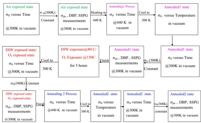
Standard measurement procedures defined in Fig. 1 were carefully applied for reliable characterization of reversible and irreversible changes, which was based on the recording of time dependent dark conductivity until it reaches a steady-state value, as “sample in high vacuum” after each treatment procedure and as annealing continues. Then, steady-state measurements of SSPC, SSPG and DBP were performed in order to detect the changes in the conductivities, minor-ity carrier diffusion lengths as well as the sub-bandgap absorption spectrum. SSPC and SSPG measurements were performed using He–Ne laser light with different intensities. DBP measurements were carried out using ac monochro-matic light with energy between 0.6 eV and 2.2 eV and a red dc bias light with different intensities [27]. Silver paral-lel electrodes were evaporated on the samples with 0.05 cm width and 0.5 cm length and a dc voltage in the Ohmic region of the current–voltage curve was applied between the electrodes during the measurements.
Relative DBP spectrum, YDBP = σac(hν)/Flux(hν), of thin
amorphous silicon films deposited on the smooth glass sub-strate is directly proportional to the absolute optical absorp-tion coefficient, α(hν), spectrum at energy region below the bandgap [29]. In order to obtain α(hν) related to the defects states in the bandgap, YDBP is normalized to the absolute α(hν) spectrum obtained independently from the transmis-sion and reflection (T&R) of the same sample at a single energy around the bandgap. In this approach, interference fringes of YDBP must be eliminated appropriately [30]. Alternatively, the fringe free absolute α(hν) of the sample deposited on the smooth glass substrate can also be calcu-lated indirectly by using the YDBP and optical transmission
spectrum, T, both having characteristic interference fringes of the sample, through the optical equations provided by Ritter and Weiser [31]. Then the α(hν) at the lower energy region will be a direct consequences of the optical transition of electrons from occupied defect states to the conduction band edge as reported previously [27]. A simple approach to get a qualitative information about the density of occupied Table 1 Summary of the deposition parameters and some material properties for the samples used in this investigation. Substrate, thickness, deposition rate, gas flows, ICRS as Raman intensity ratio and EA as dark conductivity activation energy of the samples are presented
Sample ID Substrate t (nm) Deposition
Rate (nm/s) Power (W) H2 Flow (sccm) SiHFlow 4 (sccm)
ICRS (%) E A (eV)
Before treatment EAfter treatmentA (eV)
High crystalline1 Rough glass 1127 1.57 200 200 8 75 0.33 (slightly
n-type) 0.20(DIW)
High crystalline2 Rough glass 735 0.08 20 200 4 83 0.24 (slightly
n-type) 0.22(DIW) Compact1
(refer-ence sample 1) Rough glass 1057 0.20 20 200 11 54 0.49 (intrinsic) 0.23(DIW)
Compact2
defects states in the bandgap of the thin silicon films is to monitor the changes in the α(hν) values at a single energy taken in the sub-bandgap region [32]. Alternatively, the quantitative information about these defects states was either obtained by a numerical modeling of the α(hν) spectrum based on a detailed carrier generation and recombination kinetics [27] or by using a deconvolution of the α(hν) spec-trum as presented by Niu [33].
However, the highly crystalline thick silicon films used in this investigation were deposited on rough glass substrate and therefore the optical transmission spectrum could not be measured due to optical scattering. Additionally, interfer-ence fringes in the DBP spectrum disappear. Because of that, the absolute α(hν) spectrum cannot be calculated through the Ritter-Weiser optical equation [31]. In addition, independent calculation of absolute α(hν) from the T&R measurements used to normalize the relative YDBP spectrum can no longer
exists. For this reason, our investigation of reversible and irreversible effects on the gap states due to long term air and short term DIW treatment was limited to the measurements of the relative sub-bandgap absorption spectrum, which is the relative DBP yield spectrum, YDBP. The changes in the
density and distribution of gap states after the treatments are evaluated by comparison of the changes in the YDBP spectra at sub-bandgap energies of microcrystalline silicon films.
For this purpose, relative YDBP spectra of different states of
the sample are normalized to a constant number at a single energy in the high energy part of the spectrum, where no changes in the density and distribution of defect states is expected and all spectra overlap. The differences in YDBP
spectra at lower energy part of the spectrum are used for the qualitative comparisons of the changes in defect states created by different treatments. Similarly, the absolute α(hν) spectra were calculated from the raw DBP and optical trans-mission spectra, which show interference fringes, through the optical equations defined by Ritter and Weiser [31] for the reference sample2 deposited on smooth glass; however, the remaining interference in the α(hν) spectrum will prevent to derive quantitative information about the defect states. In this case, relative changes in the α(hν) values at the low energy region will reflect the changes in the defect states created after the treatments. A home developed computer software was used to collect the data in time and temper-ature dependent dark conductivity as well as in the DBP measurements.
Fig. 1 Schematic diagram of the standard measurement procedures used to investigate reversible and irreversible effects due to air, DIW and oxygen exposures of thick microcrystalline silicon films (Color figure online)
Standard Measurement Procedure to Study Metastability/lnstability Effects
Air exposed state Air exposed state Annealing 1 Proces Annealedl state c:;0 versus Time cr 0(300K) O"plı, DBP, SSPG Heating to cro versus Time Cool to cro versus Temperature
Constant measurements 440K
@440K in 300K in vacuum
@300K in vacuum @300K in vacuum vacuum
ı
DIW exposed state/ DIW exposure@80 C/ Annealedl state Annealedl state
02 exposed state
02 Exposure@l50C O"ph , DBP , SSPG c:;0 versus Time
Cool to ~ Q"o (300K)
cro versus Time measurements
for 5 hours @300K in vacuum
@300K in vacuum 300K @300K in vacuum Constant
cr0(300K) yonstant
D IW exposed state/ Annealing 2 Process Annealed2 state Annealed2 state Annealed2 state
02 exposed state
~ c:;0 versus Time t:ool to cro versus cro versus Time ao(300K) O"plı , DBP, SSPG
c;ph, DBP, SSPG
-
Temperature • measurementsmeasurements @440 K in vacuum 300K @300Kin constant
in vacuum vacuum @300K in vacuum
3 Results
3.1 Dark conductivity results
The investigation of reversible and irreversible changes in microcrystalline silicon films, created after atmospheric exposures, inert gases, oxygen as well as de-ionized water treatments, requires long pre-experimentation monitoring of the dark conductivity to obtain a reliable record of the effects on the minority and majority carrier properties measured under steady-state conditions [23]. Probe meas-urements were performed once σD remained unchanged
with time at 300 K in the high vacuum cryostat with pres-sure of 1–2 × 10⁻⁶ mbar. Thin film semiconductors with
(i) low conductivity and possibly (ii) high susceptibility of the surface to atmospheric adsorbates can show a consider-able influence of such adsorbates on the conductivity by surface band bending resulting in strong variation of the electronic transport at and near the surface which can be a major contribution for the overall sample conductivity. Therefore, it is common practice to measure such materials in an inert atmosphere or in vacuum to assure defined and reproducible film surface condition. In case highly doped (conductive), bulk materials or samples under additional carrier excitation (illumination) are measured—with much higher conductivities—this may be done also in ambient. However, this was not the case in our studies. The percent change in σD, ΔσD ((ΔσD = (σD(measurement begins)—
σD(measurement ends))/σD(measurement begins)) × 100%) during several hours of measurements was less than 10% as seen in the figures below. The sequence of treatments on the samples was the following: The samples had been stored in laboratory atmosphere in the dark for 2 years. After this and a first detailed characterizations at 300 K, the samples were annealed at 440 K in dark and high vacuum. Then two different methods to create metastabil-ity effects were applied: (i) De-ionized water treatment at 80 °C for 5 h on samples deposited on the rough glass and (ii) oxygen exposure to Reference sample 2 deposited on the smooth glass at 150 °C for 5 h. The treatment with oxygen was preferred for the samples on smooth glass to avoid sample peeling which is frequently observed when such thin films deposited on smooth glass are immersed into water. Finally, the samples were re-annealed at 440 K to remove the created metastability effects due either to de-ionized water or oxygen gas. All measurements after each treatment were performed at 300 K in high vacuum.
In Fig. 2, time dependent dark conductivity at 300 K, σD(300 K), for highly crystalline silicon films deposited under high and low growth rates and a compact silicon film with medium crystallinity, the reference sample1, are presented after each treatment. The time scale starts with
switch-on of the vacuum pump, respectively. Measure-ments in vacuum after two years of air exposure indicate that σD(300 K) reaches a steady-state level after several hours for both highly crystalline and compact silicon films. Once the steady-state conditions of dark conductivity are established, samples were carefully characterized using SSPC, DBP, and SSPG methods in detail as described below.
After characterization of the air exposed state, the sam-ples were annealed in vacuum at 440 K for more than 10 h. In this annealing step it is assumed that the material will recover from any metastable surface adsorption processes. However, possible irreversible processes during the 2 year storage at ambient would not be identified in this procedure. The time dependence of σD at the annealing temperature is
shown in Fig. 3. The two highly crystalline samples show similar annealing behavior in dark conductivity, which initially increases during several hours of the annealing and then tends to saturate reaching to a time independent Fig. 2 Time dependence of σD measured at 300 K in high vacuum
after long term air exposure, five hours of DIW treatment as well as annealed states carried out after these treatments for a highly crys-talline1 sample, b highly crystalline sample, and c compact reference sample1, on the rough glass substrate. Same symbols indicate the same state of each sample. The sample geometry used in this study is also presented in the inset of c (Color figure online)
10"" m•
e
~
10"" C 1:) 10 .. 10-' 10 .. 104e
.!:! 10"" ~ C 1:) 10 .. 10""o
DR=1.57 nm/s - high crystalline1 T=300K ı/•=o.1s AfterDIW Exposure --
-• a b DR=0.20 nm/s-* ·
Annneale 2-After DIW1/
5=0.54 - • ·After DIW ExposureRe/erence sample1 - • · Annealed 1-Before DIW
-e -After Air Exposure (2years
After Dl Exposure
500 1000
value. Dark conductivity of the compact reference sample1 showed only little change at 440 K. After this annealing step (called the annealed1 state) the samples were slowly and computer-controlled cooled to 300 K. The activation energy of the dark conductivity (EA) was calculated from
the slope of an Arrhenius plot as shown in Fig. 4. EA was 0.33 eV and 0.24 eV for high and low growth rate samples, respectively, and 0.49 eV for the reference sample1. When the temperature of the sample reached the value of 300 K, the development of σD with time was further monitored as shown in Fig. 2a, b, and c (filled square of magenta color). σD(300 K) decreases slowly within a factor of 2–3 in 15 h before reaching a steady-state value. It was made sure by careful sample-temperature monitoring that this effect is not due to a further small decrease of the sample temperature. At the end, σD(300 K) in the annealed1 state is a factor of
20–30 higher than that of the air exposed state for highly crystalline samples. In general, more compact samples with lower crystallinity and void/crack fractions are expected to be less sensitive to the exposure processes. This is consist-ent with the assumption that the first annealing step after long time air exposure brings the sample back close to its as-deposited state as concerns dark conductivity in agree-ment with previous results reported on similar but thinner (200–400 nm) material [11, 12]. For reference sample1 with medium crystallinity, very little effect on σD upon annealing after long time air exposure is observed. While this looks in agreement with another previous investigation [22], in contrast a substantial decrease in σD(300 K) was reported
after annealing of the air exposed state of thin (200–400 nm) compact samples with similar crystallinity [11, 12].
To address such partly conflicting results by reliable, reproducible and accelerated simulation of the metastability effects upon exposure of µc-Si:H to ambient atmosphere, we have previously suggested a measurement cycle with expo-sure of the sample to de-ionized (DI) water at 80 °C for 60 min [19]. In the present study and based on that approach we have exposed the highly crystalline and compact micro-crystalline silicon films to DI water at 80 °C for an extended time of 5 h.
The time dependent σD(300 K) results recorded after
de-ionized water treatment (red filled circles) are also shown in Fig. 2. For both highly crystalline samples, in contrast to the air exposed state, σD(300 K) increased by more than
an order of magnitude during the first 10 h before reaching a time independent value. Stabilized σD(300 K) after
de-ionized water treatment was a factor of 20 and 5 higher than that of the annealed1 state level for high crystalline1 and Fig. 3 Time dependent σD measured at the annealing temperature
440 K after air exposure for highly crystalline samples and for the compact reference sample1 deposited on the rough glass substrate. In the inset, annealing temperature versus time is shown (Color figure online)
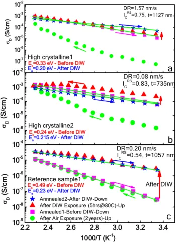
Fig. 4 Temperature dependence of σD measured in high vacuum after
long-term air exposure, five hours of DIW treatment and annealing carried out after these treatments for a highly crystalline1 sample, b highly crystalline2 sample, and c compact reference sample1, depos-ited on the rough glass substrate. Same symbols indicate the same state of each sample (Color figure online)
High crystalline1&2 •- DR= 1.57 nm/s,
1/
8=0.75 440 ı--- • DR= 0.08 n/s, le "8=0.83 •- DR=0.20 nm/s, lc"8=0.54 10-7 L . - _ _ . _ __.__....__;;_.L---ı--lL-... _ı...___. _ _J o 200 400 600 800 1000 Time(min) 10-2 DR=1.57 nm/s 10-31/
8=0.75, 1=1127 nme
104•
~••
"'
~ 10-5•• ••
•
t) 10-6 10-7 10-2 10-3-
E 10"4~
10-5-
C t:> 10-8 10"4 10-5""'--!
High crystalline1 E =0.33 ev - Before DIW E:=0.20 ev -After DIW High crystalline2 E0 =0.24 eV - Before DIW E. =0.215 ev -After DIW Reference sample1 E =0.49 ev - Before DIW ı:: =0.23 ev - After DIW• • •
•
• • • •
a
DR=0.08 nm/s RS le =0.83, t=735n... ... ...
... t
• • • •
b
t:>c*
Annnealed2-After DIW-Down10-8 .& After DIW Exposure (5hrs@80C)-Up
•
Annealed1-Before DIW-Down10-9 • After Air Exposure (2years)-Up
2.2 2.4 2.6 2.8 3.0 10001T (K1)
3.2
C 3.4
high crystalline2 samples, respectively. Now different from our expectation σD(300 K) did not recover upon annealing
after the DI water treatment. The σD(300 K) remained almost
unchanged after the second annealing process (called the annealed2 state) carried out at 440 K.
For the compact reference sample1, which did not show any change between the atmospheric gas exposure and the first annealing step, time-dependent σD (300 K) measured after de-ionized water treatment also showed an increase during the first 6 h before reaching to a stabilized level. σD(300 K) of the de-ionized water treated state was
more than two orders of magnitude higher than that of the annealed1 state. Similar to the highly crystalline samples the conductivity of the reference sample1 with medium crys-tallinity did not recover after the second annealing process performed at 440 K (Fig. 2c). From the temperature depend-ent σD(T) recorded after annealing of the DIW treated state, the slope of the Arrhenius plots yielded activation energy values, EA, of 0.20 eV and 0.22 eV for high crystalline1
and high crystalline2, and 0.23 eV for the compact refer-ence sample1, respectively (Fig. 4). Apparently both highly crystalline silicon films and the compact reference sample1 undergo an irreversible increase in dark conductivity after DIW treatment which does not recover after annealing.
It was shown earlier that DIW treatment and oxygen gas exposure at 80 °C caused similar conductivity increase on thin (200–400 nm) silicon films [20]. Considering that the reference sample2 on a smooth glass substrate with a thick-ness of 1.1 µm might peel off during the DI water exposure, we have treated this sample in an oxygen gas atmosphere for five hours at 150 °C. A temperature of 150 °C was chosen
because previous experiments on similar thick samples (≈ 1 µm) with an exposure temperature of 80 °C in oxygen have yielded very little changes in conductivity, DBP and SSPG [22].
The time dependence of σD(300 K) for the reference sample2 is presented in Fig. 5. Similar to the results of the reference sample1 shown in Fig. 2c, there was no change in σD(300 K) upon annealing after long term air exposure. In addition, after 5 h of oxygen exposure at 150 °C, the σD(300 K) measured in vacuum initially is very similar to the state after air exposure or after the annealing1 step. How-ever, upon continuous measurement, σD (300 K) increases slowly to reach a time independent value after more than 1000 min. While such an increase in σD(300 K) during
meas-urement after oxygen exposure was reported earlier [22, 23], the amount of increase by a factor of 20 from the annealed1 state is significantly higher than the results obtained after oxygen exposure carried out at 80 °C on similar quality thick intrinsic silicon films [22]. After this increase in σD(300 K)
upon measurement in vacuum after the oxygen exposure the final σD(300 K) state reached does not change anymore after an additional annealing step. Temperature dependence of σD
for the reference sample2 is shown in Fig. 6, where the slope of Arrhenius plot gives an activation energy, EA = 0.58 eV before oxygen exposure and 0.40 eV after the annealing of the oxygen exposed state.
In summary; both reference samples with medium crys-tallinity and presumed compact structure do not change their conductivity between long time air exposure and subsequent annealing. Upon treatment in DI water or alternatively in pure oxygen both finally show a considerable increase in
Fig. 5 Time dependence of σD measured at 300 K in high vacuum
after long term air exposure, five hours of oxygen gas exposure as well as annealed states carried out after these treatments for intrinsic reference sample2 deposited on the smooth glass substrate (Color fig-ure online)
Fig. 6 Temperature dependence of σD measured in high vacuum after
long term air exposure, five hours of oxygen exposure carried out at 150 °C for intrinsic reference sample2 deposited on the smooth glass substrate (Color figure online)
10-5 10-6
E
~ 10-7 C t) 10-a 10-9 DR=0.52 nm/s, 1 RS =O 69 C • t=1109 nm - - -.&.•
•
t::::==:::::=:::==
A
=>
ftel
o,
Exposureo
•
Annealed2-After O,(in SSPG)*
Annealed2-After O,(in DBP).&.- After 02 Exposure
•
Annealed1-Before 02 • After Air Exp sure500 1000 Time (min) 1500 10-3 10-4 10-6
-
E -!::! 10-6 en-
cı tı 10-7 10-8 10-9 2.2 Reference sample2 DR=0.52 nm/s1/
5 =0.69, t=1109 nm _.,.._ Annealed2- Down _._ After 02 Exposure- Up•
Annealed1- Down• After Air Exposure-Up
2.4 2.6 2.8 3.0 3.2 3.4
dark conductivity which cannot be restored by thermal annealing.
3.2 Steady‑state photoconductivity results
It was presented above that after a long time air exposure of µc-Si:H films (≈ 1 µm thickness) on glass, thermal anneal-ing leads to an increase in σD(300 K) in highly crystalline material, whereas medium crystalline material showed no difference between air exposure and annealing. Further treatment in DI water or oxygen resulted in a further strong increase in σD(300 K) for both types of materials which in all cases was not reversible by annealing. Assuming that such an increase in σD(300 K) is related to a Fermi level shift
and as a consequence to changes in the charge occupation of gap states, one would also expect direct influence on the
steady-state photoconductivity via changes in the lifetime of photo-induced charge carriers [12].
In Fig. 7, the results of steady-state photoconductiv-ity, σph, versus photon flux are shown after the long term air exposure, short-term DIW treatment as well as for the annealed states carried out after these treatments for samples deposited on the rough glass substrate. In the air exposed state, the exponent γ of the plot, σph versus photon flux, is less than unity and found to be 0.85 ± 0.02 and 0.70 ± 0.02 for high crystalline1 and high crystalline2 samples and 0.65 ± 0.02 for the compact reference sample1, respectively. In the annealed1 state, the exponent γ slightly decreased and σph measured at the photon flux of 8.0 × 1015 cm−2 s−1
increased by factor of 4 and 2 for high crystalline1 and high crystalline2 samples, respectively. Similar to its dark conductivity, σph of the compact reference sample1 showed no change after annealing of the air exposed state. Upon DI water treatment σph measured at the photon flux
of 8.0 × 1015 cm−2 s−1 increased by a factor of 20 for high
crystalline1 sample and a factor of 6 for high crystalline2 sample. A factor of 9 increase in σph was recorded for the compact reference sample 1. The exponent γ is around 0.63 ± 0.02 for the highly crystalline samples and decreased from 0.65 ± 0.02 to 0.50 ± 0.02 for the compact reference sample1. For all samples the increase in σph after DIW treat-ment was not reversible with thermal annealing.
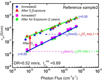
The results of σph for the compact reference sample2 are
presented in Fig. 8 after long term air and 5 h of oxygen exposure applied at 150 °C as well as for the annealed states performed after these treatments. There is little change in the σph data between long term air exposed and annealed1 states,
Fig. 7 Steady-state photoconductivity versus photon flux measured in high vacuum at 300 K after long term air exposure, 5 h of DIW treatment and annealing carried out after these treatments for a high growth rate sample, b low growth rate sample, and c reference sam-ple1, deposited on the rough glass substrate. Same symbols indicate the same state of each sample. The level of σD(300 K) for each state
is also indicated by corresponding dashed lines in color (Color figure online)
Fig. 8 Steady-state photoconductivity versus photon flux measured in high vacuum at 300 K after long term room air and five hours of oxy-gen gas exposure applied at 150 °C as well as annealed states carried out after these treatments for intrinsic reference sample2 deposited on the smooth glass substrate. The level of σD(300 K) for each state is
also indicated by corresponding dashed lines in color (Color figure online) le ss=0.83, !=735 nm b 10-4 - - - --cr0(DIW).cr0(Ann2) -________ ".ı,{Ann1). cr0(Air exp.) -High crystalline2 104 ... +-... ~ C
y=0.65 - - - -cr0(Ann1),cr0(Air exp.)
-1/3=0.54, !=1057 nm DR=0.20 n is 10-9 L-.L...L..LLlu.LIL---&....L.IU..U.LIL-...L..L..UU.WL-.L...L..LLlu.ı.ıL---&....L.LJ 1012 1013 1014 1015 1016 104 - - - . . . . - - - . - - - - ,
*
Annealed2.A. After O2Exposure
Reference sample2
•
Annealed1• After Air Exposure (2 years)
y=0.50
10-8 y=0.65
- - - a0(Ann1),cr0(Air exp.)
--9 DR=0.52 nm/s, le Rs =0.69 10 12
10 1013 1014 1015 1016 Photon Flux (cm-2s-1}
similar to the results of the compact reference sample1 pre-sented in Fig. 7c. However, high temperature oxygen gas exposure caused a factor of 6 increase in σph at the photon
flux of 8 × 1015 cm−2 s−1 and the exponent γ decreased from
0.65 to 0.50 after oxygen exposure. Again the annealing2 step after O2 exposure does not restore the σph value similar
to the results after DI water treatment (Fig. 7).
We summarize: Air exposure, DI water or oxygen treat-ment and subsequent annealing steps on µc-Si:H films result in for their σph values in qualitatively similar changes as
observed for the corresponding σD(300 K) values. The
sub-linear dependence of photoconductivity on light intensity, the exponent γ less than unity, as observed in this investiga-tion is a direct consequence of the continuous distribuinvestiga-tion of gap states located in the bandgap of microcrystalline silicon and can be explained by the model proposed by Rose [25]. When the light intensity is increased, the electron and hole quasi-Fermi levels are moved towards their respective band edges so that the higher or lower lying states are thus con-verted into recombination centers. The increased density of recombination centers decreases the carrier lifetimes and yields the sublinear dependence of photoconductivity on light intensity. Both charge state and number of gap states acting as recombination centers affect both σph values as well as the exponent γ. This should possibly show up in defect absorption spectroscopy as well as in the properties of minority carriers. For this reason, this was also studied on these µc-Si:H samples after the various treatment steps and will be presented next.
3.3 Sub‑bandgap absorption results
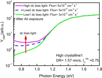
The sub-bandgap absorption coefficient spectrum obtained from the dual-beam photoconductivity (DBP) method is a powerful tool to investigate the density and distribution of gap states in amorphous silicon thin films [27], where the occupation of the gap states can be easily modified by changing the dc bias light intensity. Examples of the rela-tive DBP yield spectra, YDBP, having no interference fringes
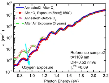
measured for different dc bias light intensities are shown in Fig. 9 for the air exposed state of the highly crystalline silicon film deposited on the rough glass under high depo-sition rate. Similarly, YDBP spectra of the compact
refer-ence sample2 deposited on the smooth glass substrate are shown in Fig. 10. Distinct fringes are seen on the YDBP and corresponding optical transmission spectra given in the inset. YDBP increases in the energy range below 1.2 eV as
the intensity of the dc bias light increases for both samples, which is related to an increase in the occupation of gap states as the quasi-Fermi levels move closer to the band edges [27,
34]. Due to the complexity of the gap state distribution in the phase mixture material µc-Si:H with possible overlaps of amorphous and crystalline silicon band structures, any
quantitative information about the types, density and energy location of these gap states cannot be easily obtained from such relative YDBP spectra, which integrate over the
contri-bution from the different structure components in µc-Si:H. However, we consider it safe to assume that the YDBP spec-trum measured under the lowest dc bias light (referred to as low1 dc bias light) corresponds to the optical transitions between the occupied gap states below the dark Fermi level and the conduction band states. For this reason, the Fig. 9 Relative DBP yield spectra, YDBP, as a function of photon
energy measured in high vacuum under different dc bias light inten-sities for the high growth rate microcrystalline silicon film after long-term air exposure. The flux of dc bias light in DBP is approx-imately 3 × 1012 cm−2 s−1 for low1, 5 × 1014 cm−2 s−1 for low2 and
5 × 1015 cm cm−2 s−1 for high dc bias light (Color figure online)
Fig. 10 Relative DBP yield spectra, YDBP, as a function of photon energy measured in high vacuum under different dc bias light inten-sities for compact reference sample2 deposited on the smooth glass after long term air exposure. The flux of dc bias light in DBP is 3 × 1012 cm−2 s−1 for low1 and 5 × 1015 cm−2 s−1 for high dc bias light
(Color figure online)
103 . . - - - ,
- -High de bias light- Flux= 5x1 O 15 em-2 s-1
::J
-e
~ 101 "' o >-10°- - Low2 de bias light- Flux= 5x10¹⁴ em-2 s-1
- -Low1 de bias light- Flux= 3x10¹² em-2~s--' ---ı
After Air exposure
High crystalline1
RS
DR= 1.57 nm/s, le =O. 75
10-1 .____.__....____.__...____._....___. ___ ...__.____.___,
0.8 1.0 1.2 1.4 1.6 1.8
Photon Energy (eV)
103- - - ,
high de bias light - Flux = 5x1 O 15 em-2 s-1
low1 de bias light- Flux = 3x10¹² em-2 s-1
102 Reference sample2 S' 101 ..ci ~ a. gı 10° >-0.8 1.0 1.2 1.4 1.6 Photon Energy (eV)
1.8 2.0
YDBP(low1) spectrum measured after different treatments will be used for the qualitative evaluation of changes in the density of occupied gap states of samples deposited on the rough glass substrate.
As already mentioned, for easier explanation and not in disagreement with other experiments, we will describe the results in the following with the assumption that our sam-ples are in general n-type with electrons as majority carriers. In Fig. 11, the YDBP(low1) spectra measured after different treatments are presented for the samples deposited on the rough glass substrates. These relative YDBP spectra were
normalized to a constant value at the energy of 1.90 eV as described at the end of Experimental Details section. Since none of the treatments do not change the density and dis-tribution of defects above the bandgap energies, all meas-urements corresponding to different treatments do overlap nicely at higher energy part of the spectrum after a nor-malization procedure as shown in Fig. 11. But significant
changes in the sub-bandgap energy region indicates that changes in defect distributions in the bandgap exist due to treatments. In the annealed1 state, the YDBP (low1) spectrum at the lower energy region at around 0.9 eV increases by a factor of 2 from the air exposed spectrum for both highly crystalline samples. For the two reference samples instead there is hardly any difference in the subgap absorption signal between the air exposed state and the state after annealing1 (see also Fig. 12).
Upon DIW treatment, the relative YDBP(low1) spectra at
energy of 0.9 eV for the highly crystalline and the reference sample1 (red filled circles) show a considerable decrease of up to one order of magnitude from the annealed1 spectrum. Finally this state (after DIW treatment) is not reversible with the second annealing step (annealed2). For the reference sample2 on smooth glass substrate, we are able to determine the absolute absorption coefficient, σ(hν), spectra from the raw YDBP and optical transmission spectra measured after
the different treatments. Similar observations are obtained for reference sample2 with O2 exposure and subsequent
annealing (Fig. 12). After O2 exposure, the α(hν)(low1) in
the subgap region around 0.9 eV decreases from annealed1 state and remains there also after annealing2 step.
As a summary, the DBP spectra of the investigated µc-Si:H samples with high and medium crystallinity show a similar qualitative response on the various treatments (long-time air exposure, DI water or O2 exposure, and annealing) as was observed for dark conductivity and photoconductivity in the sense that highly crystalline samples show changes in subgap absorption after annealing of the air exposed state and further changes after DI water treatment. Additional Fig. 11 Relative sub-bandgap absorption spectra, YDBP,
meas-ured under the lowest dc bias light in high vacuum at 300 K after long term air exposure, five hours of DIW treatment and annealing carried out after these treatments for a high growth rate sample, b low growth rate sample, and c reference sample1, deposited on rough glass substrate. Same symbols/lines indicate the same state of each sample (Color figure online)
Fig. 12 Absorption coefficient spectra obtained from the YDBP(low1)
and optical transmission spectra measured in high vacuum at 300 K after long term air exposure, five hours of oxygen exposure applied at 150 °C and annealing carried out after these treatments for intrinsic reference sample2 deposited on smooth glass substrate (Color figure online) 103. -s-1cı2 -e ~ i 101 o ...J '• >~ 100 - -Annnealed2-After DIW a
- • -After DIW Exposure(5hrs@80C)
··O· Annealed1-Before DIW
- - -After Air Exposure (2years)
High crystalline1 DR=1.57 nm/s ,
1/
8=0. 75, !=1127 nm 103r-+----+---ı---+---+---+----ı ::ı 102 -e ~ i o 101 -t.
>~ 100 ~ 102 ::ı -e ~ i 101 o ...J '• >~ 10° AfterDIW b High crystalline2 DR=0.08 nm/s ,1/
8=0.83, 1=735 n Reference Sample1 DR=0.20 nm/s , C 10-1 L"LLı..._., _ _,.. AflerDIW RS le =0.54, t=1057 nm0.8
1
1.2
1.4 1.6 1.8
Photon Energy (eV)
105
r--r----r---.---~----..--- r--r----r---.---~----..---Annealed2- After 02
104 - • - After 02 Exposure{5hrs@150C) - o- Annealed1-Before 02
103 - - After Air Exposure (3 years)
10° Reference sample2 t=1109 nm DR=0.52 nm/s Oxygen Exposure I Rs =O 69 10-1 .__...,__.___,.___.__.___,_...___ ... ___ı_c_.___JL... . ...ı.-L-....ı....J 0.8 1.0 1.2 1.4 1.6 1.8 2.0 2.2 Photon Energy (eV)
annealing after DI water treatment does not induce further changes. For the medium crystalline compact reference sam-ples no significant changes were detected between long time air exposure and the first annealing step, but similar effects on sub-bandgap absorption exist due to DI water treatment (or alternatively O2 exposure) as seen in the highly
crys-talline samples and similarly no response on an annealing step after DI water or O2 exposure has been detected. It can be concluded that DI water and O2 exposure seem to have similar effects on µc-Si:H reference samples as was also observed for the conductivity results.
3.4 Minority carrier diffusion length results
Minority carrier diffusion length, LD, in the bulk of absorber
layers in thin film silicon solar cells is one of the most impor-tant parameters for the carrier collection at the contacts and for the overall solar cell performance. The steady-state pho-tocarrier grating (SSPG) method [26] was used to investi-gate the effects of long term air exposure and short term DIW and oxygen gas treatments on the minority carrier diffusion lengths. In this method, the experimental value β = Icoh/Iincoh was recorded as a function of the experimental
grating period, Λ, as the angle θ between two light beams is altered. Here, Icoh is the ac photocurrent measured between the contacts as the polarization vectors of the laser beams are parallel and Iincoh is the ac photocurrent as the polarization
vectors of the laser beams are perpendicular. The grating period Λ is equal to λ/[2sin(θ/2)], where λ is the wavelength of the laser light. The Λ represents the distance between the fringes existing in the gap between the parallel electrodes of the sample as two coherent light beams impinge on the sample. The ratio β versus the grating period Λ was defined in the non-linear equation as
where the fit parameter ϕ defining the grating quality as ϕ = γγdγo2 (where γ is the exponent of σ
ph versus photon
flux, γd is the dark conductivity reduction factor defined as
γd = σph/(σph + σD) and γo is called the grating quality
fac-tor) and the minority carrier diffusion length LD is obtained from the best fit to the experimental data using Eq. (1) [26]. The fitting parameter ϕ is typically between 0.3 and 0.8 for the samples deposited on the smooth glass substrate [35]. However, it decreases to around 0.1– 0.2 for the samples deposited on the rough glass substrate due to higher optical scattering [36].
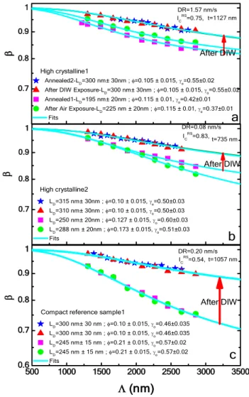
The results of β versus the grating period Λ in non-linear plots are summarized in Fig. 13a, b, and c for the 3 micro-crystalline silicon films deposited on the rough glass sub-strates. In the air exposed state, the minority carrier diffusion length LD was obtained to be 225 nm and 288 nm for high
(1) 𝛽 = 1 − 2𝜙∕(1 + 4𝜋2L2D∕Λ2)2
crystalline1 and high crystalline2 samples and 245 nm for the compact reference sample1. The values of LD obtained
for both types of samples are similar to those recently reported on the highly crystalline thick silicon films (> 1 µm) deposited on a smooth glass substrate [23]. Corresponding best fit values for the fit parameter ϕ in non-linear Eq. 1 were found to be 0.113, 0.173, and 0.210 for high crystal-line1, high crystalline2 and the compact reference sample1, respectively. The lower values of ϕ are consistent with the previous investigations carried out on similar quality silicon films deposited on rough substrates [36]. The error limits of both fit parameters, LD and ϕ, indicate in Fig. 13 that
equivalent good fits for the experimental data points can be obtained within ± 20 nm for LD and ± 0.015 for ϕ, where
Fig. 13 Experimental ratio β (symbols) versus grating period Λ of steady-state photocarrier grating method measured under dc laser light flux of 6 × 1016 cm−2 s−1 in high vacuum at 300 K after
long-term air exposure, five hours of DIW treatment and annealing car-ried out after these treatments, respectively, for a highly crystalline1 sample, b high crystalline2 sample, and c compact reference sample1, deposited on rough glass substrate. Same symbols indicate the same state of each sample. Lines are fits to the data (Color figure online)
0.9
cc. 0.8
High crystalline1
*
Annealed2-LD=300 nm± 30nm; o=0.105 ± 0.015. r,=0.55±0.020.7 After DIW Exposure-L0=300 nm± 30nm; o=0.105 ± 0.015, r,=0.55±0.0
• Annealed1-L0=195 nm± 20nm; o=0.115 ± 0.01, r,=0.42±0.01
• After Air Exposure-L0=225 nm ± 20nm; o=0.115 ± 0.01, r,=0.37±0.01
- -Fits 8 nm s 1c Rs=o.a3, t=735 nm 0.9 cc. 0.8 High crystalline2
*
L0=315 nm± 30nm; 0=0.10 ± 0.015, r,=0.50±0.03 0.7 .As LD=310 nm± 30nm; o=0.10 ± 0.015, r,=0.50±0.03 • LD=250 nm± 20nm; o=0.127 ± 0.015, r,=0.60±0.03 • LD=288 nm ± 20nm; o=0.173 ± 0.015, r,=0.51±0.03 - -Fits DR=0.20 nm/s 0.9 cc. 0.8Compact re/erence sample1
*
LD=300 nm± 30 nm; o=0.10 ± 0.015, r,=0.46±0.035 0.7 • LD=300 nm± 30 nm; o=0.10 ± 0.015, r,=0.46±0.035 • L0=245 nm± 15 nm; 0=0.21 ± 0.015, r,=0.57±0.02 e LD=245 nm ± 15 nm; o=0.21 ± 0.015, r,=0.57±0.02 O.S - -Fits 500 1000 1500 2000 2500 3000 A(nm)b
C 3500smaller values of ϕ results in larger values of LD, and/or vice versa. In the annealed1 state, LD decreased slightly by
30 nm and 38 nm for high crystalline1 and high crystalline2 samples, respectively, within the similar error limits of LD and ϕ. For the compact reference sample1, no detectable change was obtained in both LD and ϕ upon annealing after
air exposure, consistent with the results of σD, σph, as well
as the relative YDBP(low1) presented above.
The effects of DIW treatment on the LD are also presented in Fig. 13. The β vs. Λ curves show a considerable change from the data of the annealed1 state. The minority carrier diffusion length LD improved significantly from the value of the annealed1 state for all the samples investigated. It increased from 195 to 300 nm for high crystalline1 sample, from 250 to 310 nm for the high crystalline2 sample and 245 nm to 300 nm for the compact reference sample1. Both highly crystalline samples and the compact reference sam-ple1 reach to the similar values of LD after the DIW
treat-ment. Correspondingly, the fit parameter ϕ shows a further decrease towards a value of 0.10 after the DIW treatment for all the samples as presented in Fig. 13. At this level of LD and fit parameter ϕ, the accuracy of the fit to the experimen-tal data decreases. The error level of LD was estimated to be
within ± 30 nm and that of ϕ stays the same within ± 0.015. Equivalent fits can also be obtained with even lower values of the fit parameter ϕ, such as values between 0.07 and 0.1. But such lower values of ϕ results in unrealistically high values of LD.
Annealing after the DIW treatment shows no significant change in the data obtained from SSPG as seen in Fig. 13
and the extracted values for ϕ and LD remain also unchanged
within the same error limit of the fitting procedure indicated above. Therefore, similarly as observed for σD, σph and the sub-bandgap absorption, we find for the minority carrier parameter LD that it is not restored from its value after DI
water treatment with the annealing2 step.
Furthermore, the fit parameter ϕ also allows us to obtain the grating quality factor γo by using the experimental values
of the exponent γ and dark conductivity reduction factor γd obtained from the conductivity results presented above. The values of the grating quality factor γo obtained in this investigation for the highly crystalline films and the compact reference sample1 are in the range between 0.40 and 0.60 as indicated in Fig. 13. These values of γo are lower than those reported for thinner films (200–400 nm) deposited on the smooth glass [35] which can be related to the multiple internal scattering of light in thick (≈ 1 µm) highly crystal-line films in addition to the contribution of the rough glass substrate [36].
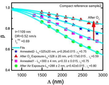
SSPG results for the compact reference sample2 depos-ited on a smooth glass are shown in Fig. 14. Better accuracy and higher values of both fit parameters, LD and ϕ, were obtained for the reference sample2, where LD was found to
be 288 nm ± 2 nm in the air exposed state and increased to 300 nm ± 4 nm after the annealing1 step. Correspondingly the fit parameter ϕ decreased from 0.42 to 0.33 upon anneal-ing of two years air exposure. Such slight improvement in LD
could be due to annealing of metastable defects not caused by the air exposure since dark conductivity, σD(300 K),
shown in Figs. 5 and 6, is almost identical in both annealed1 and air exposed states. This effect can be due to annealing of light-induced metastability [37] created in the amorphous phase of the material during the long term storage of the sample in the laboratory ambient since a slight increase upon annealing in σph was also measured in the reference sample2
as shown in Fig. 8.
Similarly observed after DIW treatment of microcrystal-line samples presented above, significant changes in both fit parameters, LD and ϕ, were measured after oxygen exposure
of the compact reference sample2. LD increased from 300 to 328 nm and the fit parameter ϕ decreased further to 0.17. At this state of sample, accuracy of the fit for LD decreases
and equivalent good fits can be obtained within ± 20 nm as ϕ changes within the same error limit of ± 0.015. After oxygen exposure there is no significant change in LD upon annealing
of the oxygen exposed state, however, the major change seen in Fig. 14 was found to be due to a significant increase of the fit parameter ϕ. It increased from 0.17 to 0.26 within the same error limit of 0.015 after annealing2 step. In contrast to that observed in microcrystalline silicon films on the rough glass substrate presented above, the grating quality factor γo
calculated from the fit parameter ϕ and other experimental parameters of γ and γd shown in the above figures are close
Fig. 14 Experimental ratio β (symbols) versus grating period Λ of steady-state photocarrier grating method measured under dc laser light flux of 6 × 1016 cm−2 s−1 in high vacuum at 300 K after
long term air exposure, five hours of oxygen exposure applied at 150 °C and annealing carried out after these treatments, respectively, for the compact reference sample2 deposited on smooth glass sub-strate. Lines are fits to the data (Color figure online)
1.0 0.8 0.6 1=1109 nm DR=0.52 nm/s
1/
8 =0.69 - FitsCompact reference sample2
*
Annealed2- L0=325±20 nm, $=0.26±0.015 ,r,=0.75A After 02 Exposure-L0=328 ± 20 nm, $=0.17±0.015, r,=0.59
•
Annealed1 - L0=300 ± 4 nm, $=0.33 ± 0.015, y0 =0.75• After Air Exposure-L0=288 ± 2 nm, $=0.42±0.015, r,=0.80 0.4 ..__..._ _ _ _ _ _ _ _ _._ _ _ _ ... _ _ _ __,
1000 1500 2000 2500 3000
to unity, indicating a much better grating quality of fringes in silicon films deposited on the smooth glass substrate [35].
Moreover, the irreversible change in LD after oxygen
exposure is consistent with the results of σD, σph, and the sub-bandgap absorption of this compact reference sample2. Further it can be inferred that both highly crystalline sili-con films and the compact reference samples deposited on rough or smooth glass substrates exhibit similar irreversible changes in their electronic properties after either DIW or oxygen gas treatment. The minority carrier diffusion length, LD greatly improves towards a value of 300 nm ± 30 nm for
all the samples investigated.
4 Discussion
For thin film semiconductors with large surface-to-bulk ratio, the effects due to adsorption by physisorption and chemisorption processes are usually considered by meas-uring electronic conductivity in vacuum and possibly after a moderate annealing step to remove surface adsorbents which would influence evaluation of the conductivity prop-erties of thin semiconductor films. This can be particularly important in case such a thin film has, in addition, a porous microstructure with openings to the surface—as is the case in some microcrystalline silicon materials. It is therefore not surprising that µc-Si:H shows reactions on the exposure to atmospheric gases or liquids as concerns the electronic conductivity or charge carrier properties in general and a number of metastability phenomena in µc-Si:H have been reported. Explanations have been suggested within the pic-tures of physisorption and chemisorption processes.
In addition to reversible adsorption processes, depending on the duration and sequence of the exposure, the treatment temperature, and the type of reactant (ambient atmosphere, DI water, pure oxygen), we have also observed non-revers-ible effects in our studies on µc-Si:H which point towards strong chemical bonds, including creation or passivation of defects which when located as electronic states in the band gaps will be similar to the surface adsorption change, charge distribution and band bending. Therefore we can in some cases have superposition or cross reaction of several effects which will make interpretation more complex.
In the following we will summarize and discuss our observation and we will try to find some common descrip-tion for the observed phenomena. And while identificadescrip-tion of microscopic origins may remain speculative, the fact that we measured a number of quantities as a function of surface exposure that will be helpful at least to focus down on pos-sible explanations.
Due to the complex nature of its microstructure, there is no standard microcrystalline silicon film with well-defined properties. Additionally, structural evolution with film
thickness is frequently observed [38, 39]. There are several structural and physical parameters to be considered when reporting the results on such films, such as crystalline vol-ume fraction ICRS, porosity, thickness, substrate type, as
well as transport properties, such as the dark Fermi level position which determines the occupation of defect states by maintaining the charge neutrality as well as defining the conductivity type of the sample. Among those parameters; crystalline volume fraction, thickness and the position of dark Fermi level seem to play the major role in determining the conductivity changes after exposure of microcrystalline silicon to different ambient conditions.
The steady-state methods using light for the probing of the metastable changes require a priori establishment of con-stant dark conductivity at concon-stant probe temperature for the accurate recording of reversible and irreversible changes in majority and minority carrier properties. In this investiga-tion, we have carefully applied the standard measurement procedures described in the Fig. 1 by monitoring of the dark conductivity as a function of time as presented in Figs. 2
and 5 before using the steady-state methods to record the changes created by long term air, 5 h of DIW and oxygen exposures as well as by the annealing performed at 440 K after these treatments [23]. Only after this established stand-ard measurement procedure shown in Fig. 1, reliable com-parison of the results obtained on different microcrystalline films due to different treatments can be made.
It was found in the present investigation that highly crys-talline about 1 µm thick microcryscrys-talline silicon films depos-ited on a rough glass substrate have an activation energy of the dark conductivity of 0.33 eV and 0.24 eV for the high crystalline1 sample prepared under high growth rate and for the high crystalline2 sample prepared under low growth rate, respectively. High crystalline silicon films even when deposited under optimum deposition rates have porous microstructure [38]. As the deposition rate increases, poros-ity and the fraction of the cracks/voids increases so that air molecules can easily diffuse through the bulk of the samples. Both reversible conductivity decreases and irreversible con-ductivity increases were observed in these highly crystalline samples. Such results on the same film were not reported before. Reversible conductivity changes occur due to storage of samples in room ambient, where both σD(300 K) and σph
of the air exposed state increased substantially after anneal-ing1 step as shown in Figs. 2, 4, and 7. It was speculated that such conductivity changes were due to the in-diffusion of air molecules, mainly oxygen and H2O, adsorbed physically on
the surface of crystalline grains [14], which induced surface charge on the surface of grains and the Fermi level moved away from the conduction band edge to maintain the charge neutrality. Annealing1 step removes the physically adsorbed oxygen and/or H2O from surface of grains and the Fermi level shifts back towards the conduction band edge causing
an increase of both σD (300 K) and σph for these highly crys-talline samples as presented above in Fig. 4a and b as well as an increase in the density of occupied defect states below the Fermi level. This is consistent with the results of the sub-bandgap absorption spectra measured under the lowest dc bias light DBP measurement, where YDBP(low1) spectrum
of the annealed1 state at the energy of 0.9 eV was higher by a factor of 2 from the air exposed state as shown in Fig. 11a and b.
The second effect observed in these highly crystalline materials is an irreversible conductivity increase from the annealed1 state after DIW treatment. σD(300 K) increased by factor of 20 and 5 for high crystalline1 and high crys-talline2 samples, respectively. Such increase in σD(300 K)
can only be possible if the dark Fermi level shifts towards the conduction band edge. It was found from the activation energy results of the dark conductivity given in Fig. 4 that the EA, measured after DIW treatment, decreased to a value
of 0.22 ± 0.02 eV for both samples. Such shift of the dark Fermi level will also increase the photoconductivity and decrease the exponent γ [40] as observed in Fig. 7a and b. In addition, large increase in σph should also imply that the
den-sity of recombination centers in the bandgap should decrease after DIW treatment. The results of sub-bandgap absorption shown in Fig. 11a and b confirm that almost an order of magnitude decrease in the YDBP(low1) spectrum at energy of
0.9 eV was recorded from the annealed1 state spectrum for both highly crystalline films. Such decrease in YDBP(low1) indicates that density of occupied defect states below the Fermi level decreased substantially after DIW treatment and became irreversible after annealing of the DIW exposed state. A large decrease in the density of occupied gap states below the Fermi level cannot be due to a shift of the Fermi level towards the midgap since it moved towards conduction band edge. This implies that water molecules made chemical bonding with the defects on the surface of crystalline grains causing a reduction in the defect density as well as a shift of Fermi level towards the conduction band edge.
The reversible and irreversible effects observed in the results of conductivities and sub-bandgap absorption of highly crystalline microcrystalline silicon samples can also be related to the changes in the minority carrier diffu-sion lengths, LD. Long term air exposure results in a small
amount of increase in LD for both samples due to a decreased density of occupied defect states. As presented in Fig. 13a and b, LD in the air exposed state is 30 nm higher than that
of annealed1 state for high crystalline1 sample and 38 nm higher for the high crystalline2 sample. The cycle between air exposure and annealing also demonstrates reversibility in LD measurements in our previous investigations [21, 23].
After DIW treatment, LD increased further to a value of
300 nm ± 30 nm from the annealed1 state level and became irreversible after annealing of the DIW exposed state.
Significant amount of improvement in LD indicates that the density of recombination centers for the minority carrier holes located between the valence band edge and the hole quasi-Fermi level decreased by a detectable amount. This was qualitatively confirmed by the results of the sub-band-gap absorption spectra presented in Fig. 11a and b for these highly crystalline microcrystalline silicon samples.
Investigation of reversible and irreversible changes in thick highly crystalline silicon films was extended to thick compact reference samples with similar thicknesses, which have intrinsic conductivity with activation energy of dark conductivity larger than 0.49 eV before exposing to DIW or oxygen. Since the best solar cell efficiency values were reported with such compact absorber layers having mixture of amorphous and crystalline regions [2, 41, 42], it is sci-entifically and technologically important to investigate the effects in such thick absorber layers. In the present investi-gation, one of the compact reference samples had crystal-line volume fraction of ICRS = 0.52 and was deposited on the
rough glass substrate. The second one was prepared on a smooth glass substrate with ICRS = 0.69. As recently reported
by Michard et al., thick (~ 700 nm) compact microcrystalline silicon films deposited under similar conditions of our com-pact reference samples do not show significant in-diffusion of oxygen after six months of storage in air as measured by FTIR and SIMS methods [43]. The results on thick com-pact reference samples obtained in this study also showed undetectable changes between the measured σD (300 K), σph, SSPG and sub-bandgap absorption results of the annealed1 and long term air exposed states as presented above, which are also consistent with our recent report on thick (> 1 µm) intrinsic microcrystalline silicon films with varying crystal-line volume fractions [22].
However, DIW treatment for the reference sample1 and high temperature oxygen gas exposure for the reference sample2 created the same irreversible conductivity increase in such a short time of five hours. Orders of magnitude increase in both σD(300 K) and σph were observed and that
the activation energy of samples EA decreased from 0.49 eV
to 0.23 eV for the reference sample1 and from 0.58 eV to 0.40 eV for the reference sample2. Such improvement in σph correlates well with the results of sub-bandgap absorption, where a significant decrease at the energy of 0.9 eV was observed after the treatment of compact reference samples as presented in Figs. 11c and 12, respectively. The change in sub-bandgap absorption became almost irreversible after the annealing. Such decrease in the density of occupied defect states below the Fermi level leads to a significant reduction of the density of recombination centers for the minority car-rier holes, which finally improved the minority carminority car-rier dif-fusion length, LD. Similarly observed in highly crystalline
silicon films, LD showed an increase towards the value of 300 nm ± 20 nm after the treatments and became irreversible