INVESTIGATION ON ELECTRICAL CHARGING/DISCHARGING PROPERTIES OF THIN PS/PMMA POLYMERIC FILMS BY DYNAMIC X-RAY PHOTOELECTRON
SPECTROSCOPY
A THESIS
SUBMITTED TO THE DEPARTMENT OF CHEMISTRY
AND THE INSTITUTE OF ENGINEERING AND SCIENCES OF BİLKENT UNIVERSITY
IN PARTIAL FULFILLMENT OF THE REQUIREMENTS FOR THE DEGREE OF
MASTER OF SCIENCE
By
HİKMET SEZEN May 2008
II
I certify that I have read this thesis and that in my opinion is it is fully adequate, in scope and quality, as a thesis of the degree of Master in Science
……….. Prof. Dr. Şefik Süzer (Principal Advisor)
I certify that I have read this thesis and that in my opinion is it is fully adequate, in scope and quality, as a thesis of the degree of Master in Science
……….. Prof. Dr. Ergin Atalar
I certify that I have read this thesis and that in my opinion is it is fully adequate, in scope and quality, as a thesis of the degree of Master in Science
……….. Assoc. Prof. Dr. Margarita Kantcheva
III
I certify that I have read this thesis and that in my opinion is it is fully adequate, in scope and quality, as a thesis of the degree of Master in Science
……….. Assist. Prof. Dr. Erman Bengü
I certify that I have read this thesis and that in my opinion is it is fully adequate, in scope and quality, as a thesis of the degree of Master in Science
……….. Dr. Gülay Ertaş
Approved for the Institute of Engineering and Sciences
……….. Prof. Dr. Mehmet Baray
IV
ABSTRACT
INVESTIGATION ON ELECTRICAL CHARGING/DISCHARGING
PROPERTIES OF THIN PS/PMMA POLYMERIC FILMS BY DYNAMIC X-RAY PHOTOELECTRON SPECTROSCOPY
HİKMET SEZEN M.S. in Chemistry
Supervisor: Prof. Dr. Şefik Süzer May, 2008
Electrical charging/discharging properties of thin layers of spin coated pure PS polystyrene (PS), and pure poly(methyl methacrylate), (PMMA) and an immiscible PS/PMMA blend are studied with externally applied DC and dynamic(squarewave stress) X-Ray Photoelectron Spectroscopy (XPS).
PS and PMMA exhibit quite different charging properties under DC stress. Due to the different charging properties of PS and PMMA domains within an immiscible PS/PMMA blend film, charge contrast or phase separation is clearly observed between domains.
V
Electrical parameters of PS and PMMA thin films while employing a squarewave pulse stress in a 10-3 - 103 Hz range of frequency are probed by dynamic XPS. A model, which can simulate the dynamical XPS measurements, is shown to lead to obtain effective resistance and capacitance values for each polymer. RC time constants and inflection points(frequency) are also determined. Moreover, thickness also affects the charging/discharging properties and other electrical parameters of polymeric thin films. Furthermore, to mimic certain dielectric properties of thin polymeric films and to validate our model, we have included an externally RC circuit to a conducting graphite sample under both DC and squarewave pulse stresses.
Keywords: XPS, Dynamic XPS, Charging, Differential Charging, Time Constant, Charge Contrast, Phase Seperation, Simulation.
VI ÖZET
İNCE PS/PMMA POLİMER FİLMLERİNİN ELEKTRİKSEL ÖZELLİKLERİNİN
DİNAMİK XPS İLE İNCELENMESİ
HİKMET SEZEN Kimya Yüksek Lisans Tezi Danışman: Prof. Dr. Şefik Süzer
Mayıs, 2008
İnce-kaplama methoduyla hazırlanmış saf polistiren (PS), poli(metil metakrilat) (PMMA), ve karışım PS/PMMA polimer filmlerinin elektriksel özellikleri X-ışını fotoelektron spektroskopisi (XPS) ile dışarıdan doğrusal voltaj ve dinamik(kare dalga) uygulanarak incelenmiştir.
PS ve PMMA farklı yüklenme özellikleri olmasından yola çıkılarak, karışım PS/PMMA polimer filmi yüzeyindeki saf PS ve PMMA bölgelerinin birbirilerine göre farklı yüklenme özellikleri olduğundan yük ayrışımı ve/veya faz ayrışımı açık bir şekilde XPS’e dışarıdan doğrusal voltaj uygulamasıyla ölçülmüştür.
VII
10-3 - 103 Hz frekans aralığında dışarıdan uygulanan kare dalga ile ince-kaplama PS ve PMMA polimer filmlerinin eletriksel parametreleri dinamik XPS ile incelenmiştir. Geliştirilen bir modelle etkin direnç ve kapasite değerleri her bir ince-kaplama ile hazırlanmış polimer filmleri için saptanmıştır. XPS ölçümlerini modelleyebildiğimiz method ile ince polimerik filmlerin etkin direnç ve kapasite değerleri saptanmıştır. Ayrıca aynı method ile bu filmlerin zaman sabitleri ve bükülme frekanları hesaplanmıştır. Bunun yanında, polimer film kalınlıklarının yüklenme ve diğer elektriksel parametrelere olan etkileri incelenmiştir. Son olarak, modelin geçerliliğini denemek ve polimerik filmlerin dışardan doğrusal voltaj ve kare dalga uygulamalarındaki dielektiksel davranışlarını simüle edebilmek için, değerleri bilinen ve dışarından paralel bağlanmış direnç ve kapasite içeren devre elemanı ile iletken bir grafit numunesinde de ölçümler yapılmıştır.
Anahtar Kelimeler: XPS, Dinamik XPS, Yüklenme, Diferansiyel Yüklenme, Zaman Sabiti, Yük Ayrışımı, Faz Ayrışımı, Modelleme.
VIII ACKNOWLEDGEMENTS
This short, but comprehensively scientific survey more than for achieving my master thesis is an enjoyable period of my life, and an impressive preface of my academic carrier. The most probable reason of that the great interaction with my supervisor, Prof. Dr. Şefik Süzer, for the duration of the period. I am aware of the privilege of work with my supervisor, and so I have my deepest thankfulness to him.
I would also like to deepest thanks to Dr. Gülay Ertaş, who also supervised me during each step of my master work. I also thanks to Aykutlu Dâna, who has a significant role to complete my thesis.
Thanks to previous and current Süzer-lab members; Ferdi Karadaş, Korcan Demirok, Bora İnci, Hacı Osman Güvenç, İlknur Kaya-Tunç, Eda Özkaraoğlu, Pınar Cönger, Engin Karabudak, Hatice Başbuğ, Sinem Yılmaz, and Sevnur Kömürlü.
I would like to show appreciation to my dear friends for moral support without any remuneration; Cemal Albayrak, Yüksel Alan, Oğuzhan Çelebi, Mustafa Fatih Genişel, Yurdanur Türker, Ünsal Koldemir, H. Burak Tiftik. Also a special thanks to Ethem Anber, Emine Yiğit, and Hüsnü İçer.
I always feel myself indebted to Bilkent University and Chemistry Department for providing highly equipped education and research opportunity.
Finally, I want to express my deepest gratitude to my family and my love Feriza Özkuzucu if I can.
IX
TABLE OF CONTENTS
1. INTRODUCTION... 1
1.1. X-Ray Photoelectron Spectroscopy (XPS) ... 1
1.1.1. Principles... 1
1.1.2. Common Application Areas of XPS... 6
1.1.2.1. Elemental Identification ... 6
1.1.2.2. Chemical State Identification ... 8
1.1.2.3. Quantification... 10
1.1.2.4. Depth Profiling... 11
1.1.2.4.1. Nondestructive Depth Profiling ... 11
1.1.2.4.1.1. Angle Resolved XPS(ARXPS) ... 11
1.1.2.4.2. Destructive Depth Profiling ... 13
1.1.3. Charging Issue in XPS Measurement ... 14
1.1.3.1. Controlled Surface Charging... 15
1.1.3.2. Theory and Modeling of Dynamic XPS... 18
2. AIM OF THE WORK ... 23
3. EXPERIMENTAL... 24
3.1. Surface Coating... 24
3.2. Preparation of Thin PS and PMMA Films on Si Wafers... 27
3.3. Instruments and Techniques ... 28
X
3.3.2. Dynamic XPS... 28
3.3.2.1. The Software for Simulating the Dynamic XPS ... 30
3.3.3. External RC... 30
3.4. Monitoring the Layer Thickness of SiO2 Using XPS and FT-IR ... 30
4. RESULTS AND DISCUSSIONS ... 34
4.1. Applying External DC Voltage Stress to Polymeric Thin Films... 34
4.1.1. Phase Separation of Thin PS/PMMA Blend Film ... 41
4.2. Applying Square Wave Pulse for Monitoring Frequency Dependence of Thin Films ... 43
4.2.1. Extracting Electrical Information of Thin Film via Software... 48
4.2.1.1. Fitting Resistance and Capacitance Values of Thin Polymer Films ... 48
4.2.1.2. RC Time Constant and Determination of the Inflection Frequency of Thin Polymeric Films ... 50
4.3. External RC... 57
4.3.1. Mimicking Dielectric Behavior of Polymeric Films ... 57
5. CONCLUSIONS ... 62
XI
LIST OF FIGURES
Figure 1. Basic principles and components of XPS experimental set-up. ...2
Figure 2. Schematic diagram of the energy levels...3
Figure 3. Photoelectric effect due to X-Ray radiation. ...4
Figure 4. Schematic representation of the photoelectric effect...4
Figure 5. An example of a typical XPS spectrum of fluorinated organosilane, FTS, on a Si substrate. ...7
Figure 6. The XPS spectrum of 2p region of SiO2/Si sample...9
Figure 7. The conventional and angle resolved XPS set-ups...12
Figure 8. The angle resolved XPS spectrum of a SiO2/Si sample. ...13
Figure 9. Charging processes in (a) convinus a conductive and (b) a nonconductive material during recording of XPS data. ...15
Figure 10. The XPS spectra of 2p regions of SiO2/Si sample under (a) -10 V and (b) +10 V DC stress with varying e-gun currents...17
Figure 11. Schematic representation of the charging and developed potential of surface structure of nonconductive SiO2 layer under (a) -10 V and (b) +10 V DC stress with varying the current level of the low-energy electron flow. ...18
Figure 12. (a) The circuit for the simulation of dynamic XPS system and (b) theoretically calculated lineshape functions at different frequencies.34...19
Figure 13. (a) Calculated lineshape functions at 1 Hz and 0.001 Hz for an 8.2 MΩ and 1µF resistance and capacitance values. (b) Grounded XPS spectrum of a graphite sample. (c) Experimentally measured and theoretically calculated XPS spectra of the graphite sample connected with an external RC (8.2 MΩ and 1µF) circuit, and also shown on offset corrected calculated spectra. (d) Schematics diagram of the experiment set-up. ...21
XII
Figure 14. Dependence of the calculated peak broadening on squarewave pulse frequency of the graphite + RC unit sample(dotted line) and measured XPS spectra of C1s of this sample(solid lines) at three different pulse
frequencies: 0.001 Hz, 0.018 Hz, and 1 Hz with FWHM values. ...22
Figure 15. The preparation of thin polymeric films via spin coating technique...25
Figure 16. The procedure of dip coating technique. ...26
Figure 17. The schematic diagram of a typical, DC biased, and dynamic XPS set-up. ...29
Figure 18. (a) The area of FTIR peak of SiO2 layers versus annealing times. (b) The baseline corrected FTIR spectra of Si/SiO2 samples at different oxide thicknesses. ...31
Figure 19. XPS spectra of Si/SiO2 systems with various thicknesses of the SiO2 layers...32
Figure 20. XPS spectra of C1s regions of a graphite sample connecting to ground, and subjected to -10 V, and +10 V external DC stresses. ...35
Figure 21. C1s region of XPS spectra of thin PMMA film on Si substrate, when the sample is grounded and under +10 V DC stress both without electron gun, and +10 V DC with 3.0 A current of e-gun, +10 V DC and 3.2 A current of e-gun. +10 V corrections are done by subtracting 10 eV from binding energy axes of spectra. A model of experimental set-up(left) and deconvoluted C1s of envelop PMMA(right) are shown in the insets of Figure. ...36
Figure 22. (a) After bias correction on XPS spectra of C1s regions of thin PS film, and (b) C1s and (c) O1s regions of thin PMMA film on a Si wafer while connecting ground, subjecting -10 V, and +10 V DC bias. ...39
Figure 23. (a) XPS spectra of deconvoluted C1s and O1s envelopes of PMMA. (b) The measured surface charging on each sub-peak of C1s and O1s as a function of the applied external bias in the presence of 3.0 A e-gun current. ...40
XIII
Figure 24. The XPS spectra of C1s regions of thin PS, PMMA and blend PS/PMMA films under (a) +10 V, (b) -10 V DC stress, and (c) grounded without bias correction. ...43 Figure 25. The C1s region of XPS spectra of (a) graphite, (b) PS(ca. 20 nm) and (c)
PMMA(ca. 20 nm) thin films when samples are grounded and subjected to ±10 V squarewave pulses at 1 Hz and 0.001 Hz. The inset shows experimental set-up of the dynamic XPS...45 Figure 26. Frequency dependences of measured binding energy difference of thin PS
(ca. 20 nm), PMMA(ca. 20 nm), and immiscible PS/PMMA(ca. 15 nm) blend films. ...47 Figure 27. (a) Frequency dependence of the measured binding energy difference of
thin PS film and calculated binding energy differences at same resistance, but with different capacitance values. The arrow shows direction of the increment in the capacitance value. (b) Calculated broadening behaviors corresponding to these resistance and capacitance values. The solid lines are theoretically calculated and the line+symbol is the experimentally measured values plotted in a semilog fashion...49 Figure 28. Frequency dependences of the measured binding energy difference of 20
nm, and 55 nm of thinner and thicker PS films in a semilog fashion, (b) calculated peak broadening behavior of this PS film. The solid lines are theoretically calculated data in both (a) and (b)...52 Figure 29. (a) The C1s region of XPS spectra of thin PS(ca. 20nm) film under
squarewave pulse at different frequencies, (b) when it is grounded, and subjected under -10 V, and +10 V DC stresses without any bias correction...53 Figure 30. (a) C1s region of XPS spectra of PS thicker (ca. 55nm) film under
squarewave pulse at different frequencies, (b) C1s region of XPS spectra of PS thicker (ca. 55 nm) film (c) and of PS thinner (20 nm) film when is connected to ground, and subjected to -10 V and +10 V DC stresses...54
XIV
Figure 31. Frequency dependence of 20 nm of PMMA film of measured binding energy difference in a semilog fashion, (b) calculated peak broadening behavior of PMMA. The solid lines are theoretically calculated data in both (a) and (b)...55 Figure 32. (a) C1s region of XPS spectra of PMMA thin film under squarewave pulse
at different frequencies, (b) when connected ground, and subjected under -10 V, and +-10 V DC stresses without any bias correction. ...56 Figure 33. (a) C1s region of XPS spectra of PS (20 nm) film (b) of graphite + RC
when connected ground, and subjected -10 V and +10 V DC stresses. The inset shows experimental set-up for the purpose of mimicking. ...58 Figure 34. (a) Frequency dependence of graphite only, graphite + RC, and PS(20nm)
film. (b) C1s spectrum of graphite + RC subjected to ±10 V squarewave pulses at 1 Hz and 0.001 Hz...59 Figure 35. (a) Frequency dependence of theoretically calculated and measured of two
samples of graphite + RC with different resistance and capacitance values, (b) theoretically calculated broadening activities of both these two graphite samples...60
XV
LIST OF TABLE
1
1. INTRODUCTION
1.1. X-Ray Photoelectron Spectroscopy (XPS)
X-Ray Photoelectron Spectroscopy (XPS), is one of the most powerful methods for surface analysis, which is also known as ESCA, Electron Spectroscopy for Chemical Analysis. XPS technique was firstly developed by Kai Siegbahn, who was awarded with the Nobel Prize for his crucial contributions in electron spectroscopy in 1981, and has been in use intensively since 1970s.1, 2 The reason, that XPS is a popular surface analysis technique, is due to its relative simplicity, and ability in deriving chemical information from the peak positions with a perfect precision and sensivity.
1.1.1. Principles
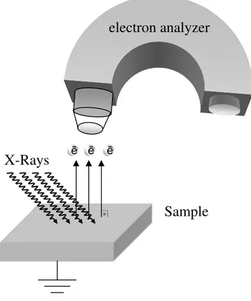
As illustrated in Figure 1, XPS analysis is based on determination of the kinetic energy of emitted electrons using an electron energy analyzer. The binding energy of the emitted electrons is obtained by using the Einstein’s relation;
2
Figure 1. Basic principles and components of XPS experimental set-up.
where BE refers to the binding energy, KE to the measured kinetic energy of photoelectron, and hυ is the energy of X-Ray photons. Ф is the work function, which is the minimum required energy to remove one electron from an atom in a solid to the vacuum level as demonstrated in Figure 2.
The work function, Ф, is usually eliminated from Equation 1 because the binding energies of photoelectrons are mostly tabulated by referencing to their Fermi levels rather than vacuum level2 and Equation 1 becomes simpler;
BE= hυ – KE (2)
X-Rays
ē ēSample
electron analyzer
ē •3
Figure 2. Schematic diagram of the energy levels.
The analytical value of the binding energy includes characteristic information about specific signals of the corresponding atoms. In the light of foregoing, the classifying XPS signals provide chemical and physical information of a few outer atomic layers of the sample due to photoelectric effect. However, X-Rays can reach 1-20 µm depth into the sample, the probe length of XPS is approximately 10-20 nm, which essentially depends on the type of X-Ray source and the sample. Photoelectric effect, as shown in the Figure 3 and 4, was discovered by Hertz and explained by Einstein in early 1900s.3, 4 Photoelectrons are preferentially ejected from core(inner) levels instead of valance or outer levels as a consequence of better matching between the wavelength(or energy) of X-Rays and the energy levels of the core electrons as represented in Figure 4.
Ф
work functionK
L
1L
2,L
3M
Valance band
Fermi level, E
fVacuum level, E
vX-Rays
1s
2s
2p
3s,p,d
4
Figure 3. Photoelectric effect due to X-Ray radiation.
Ne0 or O2- Ne+1 or O1-
Figure 4. Schematic representation of the photoelectric effect.
ē ē ē ē ē ē ē ē ē X-Rays ē
d
I
ē1-20 µm
Sample
ēI
0ē ē
X-Rays
scattered electron
ēphotoelectron
ēK.E.
ē ē ē ē ē ē ē ē ē ē excited electron of Ne or O 1s5
However, generated photoelectrons can not survive due to inelastic collisions with other atoms in the solid. This is the reason why only a depth length of 10-20 nm is accessibly by the XPS technique. This range is governed by the characteristic value of attenuation length (AL) or inelastic mean free path (IMFP) of the substance, which is usually represented by “λ”. The IMFP is defined as the average traveling distance of a beam of photoelectrons where the intensity of photoelectrons decay by 1/e of their initial intensity due to both elastic and inelastic collisions which cause them to lose kinetic energy and/or to change direction. The relationship is expressed by Equation 3 and demonstrated also in Figure 3.
I/I
0=e
-d/λ(3)
The AL or IMFP is also a function of the kinetic energy of photoelectrons.5-7According to the above expression, after traveling along just one λ path length, 63% of photoelectrons are already scattered from their original route. Therefore, using XPS one has a chance to detect photoelectrons having kinetic energy to travel at most 3 λ length, which corresponds to more than 95% scattering, in the solid to reach the surface of the sample.
Thus, with such an extremely short depth length, 10-20 nm, XPS emerges as a crucial surface sensitive technique and it perfectly matches today’s demanded technologic requirements for analysis in the nanometer scale. Moreover, the surface sensitivity of XPS can be boosted up by changing the receiving angle of photoelectrons with respect to the surface plane of the sample. This technique is named as Angle Resolved XPS8-11 and will be introduced later. However, such a surface sensivity may also become disadvantageous in some cases. For instance, a 10 nm depth length corresponds to just a few atomic layers
6
where one or more contaminant layers on each surface are always present. Hence, extreme care must always be practiced to ensure correct analysis results.
1.1.2. Common Application Areas of XPS
Application areas of XPS technique can be listed as:2 - Elemental Identification
- Chemical State Identification - Quantification
- Depth Profiling
1.1.2.1. Elemental Identification
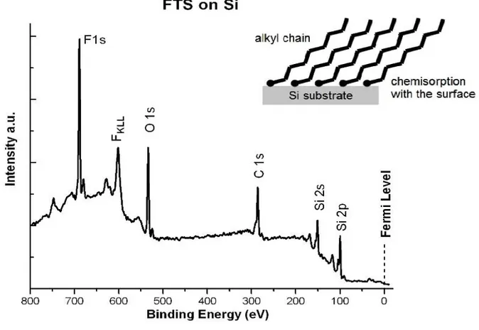
XPS is commonly used to investigate the surface of samples. The value of peak position (binding energy) of particular photoelectrons provides straightforward elemental identification of atom(s) from which electrons are emitted, with the exceptions for hydrogen and helium elements. The value of binding energy not only notifies information on classifying the identity of an atom, but also it provides information about orbital of atom from which photoelectron is emitted. For example, the binding energy around 100 eV corresponds to 2p level of Si, 151 eV corresponds to 2s of Si, 285 eV corresponds to 1s of C, 532 eV corresponds to 1s of O, and 690 eV corresponds to 1s of F on the XPS spectrum which is plotted as the counted signal intensity versus corresponding binding energy as
7
shown in Figure 5. The spectrum shown in Figure 5 is a self-assembled layer of eight fluorinated carbon membered organosilane, tridecafluoro-tetrahydrooctyltriethoxysilane (FTS), on a Si substrate.
Figure 5. An example of a typical XPS spectrum of fluorinated organosilane, FTS, on a Si
substrate.
In addition to the qualitative information from the peak position, the multiplicity of peaks may also provide extra information on elemental identification during an XPS survey. For instance, the spin orbit splitting, which occurs for peaks of p, d, and f orbitals where these peaks on the XPS spectrum are present as two separated peaks, doublets, are
8
characteristics of each element. Moreover, the relative area ratios between two spin-orbit peaks have distinct values for each p, d, and f orbitals as 1:2, 2:3, and 3:4, respectively. Therefore, the value of area ratios is valuable for categorization of the peaks. Furthermore, the absolute value of the spin orbit splitting also offers information for elemental recognition since this value is specific to each element and orbital. The full width at half maximum, FWHM, can also give information about the homogeneity of sample. A small value of FWHM may indicate comparatively more homogeneous substance than a larger FWHM value, which may indicate more than one derivative of that element in the sample.
1.1.2.2. Chemical State Identification
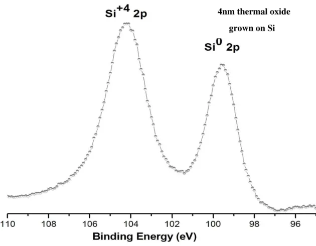
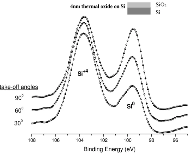
XPS technique also allows for the determination of the chemical state of the atoms on the analyzed surface. Different chemical states of atoms of the same element in a sample may manifest as shifts in the binding energies. For example, different oxidation states may induce changes in the energy levels of core electrons in atoms, and as a result, during photoemission process the kinetic energies of emitted electrons from core levels are affected accordingly. This shift is called “chemical shift”. For instance, the binding energy of Si 2p varies according to oxidation state of Si as shown in Figure 6 and tabulated in Table 1.
9
Figure 6. The XPS spectrum of 2p region of SiO2/Si sample.
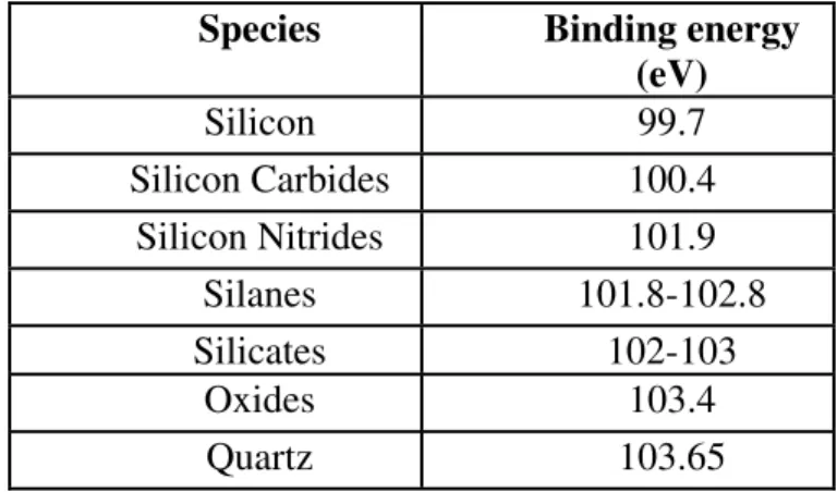
In Figure 6, the XPS spectrum from a 4 nm thermal oxide grown on Si indicates two separated peaks for Si. The electrons in Si atom at +4 oxidation state feel a stronger positive charge, so that the 2p photoelectrons have smaller kinetic energy and as a consequence of Equation 2 they have higher binding energy. Similarly, for the photoelectrons emitted from an atom with a net negative charge binding energy of photoelectrons shift toward lower binding energies. In addition, the potential developed by the adjacent atoms or environment also affects the chemical shifts as shown in Table 1 for silicone.
4nm thermal oxide grown on Si
10
Table 1. The binding energy value of Si 2p peaks of different silicon compounds.2, 12
Species Binding energy
(eV) Silicon 99.7 Silicon Carbides 100.4 Silicon Nitrides 101.9 Silanes 101.8-102.8 Silicates 102-103 Oxides 103.4 Quartz 103.65
1.1.2.3. Quantification
The qualitative analysis of the surface of the specimen is directly derived from the elemental analysis by XPS. The quantitative information is achieved by calculating the relative atomic ratios of the sample surface in a range of 1 to 20 nm using the area of the peaks. However, other parameters contribute to this analysis as well. In general, the following formula is used for this purpose:2
[ ]
[ ]
3
2
k
y
y
x
k
y
x
x
y
x
E
C
C
E
A
A
=
σ
σ
(4) Here, A is the area of the corresponding photoelectron peak,σ
is the cross section of the corresponding orbital, and Ek is the kinetic energy of the photoelectron peak. Using11
Equation 4, an average empirical formula of the sample surface can be evaluated. This can also be used to obtain information about preferred orientation of molecules or functional groups at the surface.
1.1.2.4. Depth Profiling
Depth profiling refers to the compositional analysis along the perpendicular direction to the surface plane of the sample and can be conducted using nondestructive and/or destructive methods.
1.1.2.4.1. Nondestructive Depth Profiling
Angle resolved X-Ray Photoelectron Spectroscopy, ARXPS, is a common technique to perform nondestructive depth profiling with XPS.
1.1.2.4.1.1. Angle Resolved XPS(ARXPS)
Since XPS is a surface sensitive technique and by changing the orientation of the sample with respect to the energy analyzer, the surface sensitivity can be further enhanced down to 1-2 nm levels. The experimental set-up for Angle Resolved X-Ray Photoelectron Spectroscopy, ARXPS, is demonstrated in Figure 7.
12
Figure 7. The conventional and angle resolved XPS set-ups.
In Figure 8 an application of ARXPS of the SiO2/Si system is shown. The XPS spectrum from an approximately 4 nm thermally grown oxide layer on silicon, is depicted at 3 different take-off angles(θ); 900, 600, and 300. The take-off angle can be defined as the angle between the surface plane of sample and the electron energy analyzer. Relative intensity of the upper layer(Si+4), Iθ, increases going down to lower angles as given by the Equation 5:2
I
θ= I
(θ =90)/
sinθ
(5)As shown in Figure 8, when the sample of SiO2/Si system is tilted from 900 of take-off angle, the relative intensity of 2p region of Si0 decreases while the peak intensity of 2p region of Si+4 increases due to arrangement of layers. Additionally, the uniformity of top layer can be assessed by ARXPS to resolve if any distortion is present in the 1-2 nm level of the sample. This is an important tool for analysis of macromolecules13 or composites14 containing two or more species to reveal the enrichment of one of the functional group(s)
.
X-Ray
e
-45
0d
Sample
θ
=90
0X-Ray
e
θ<90
0d
'
d
'
=
d sin θ
Sample
13
or element(s) on the surface. The ARXPS could also be utilized for assessing morphological structure of surfaces.15, 16
Figure 8. The angle resolved XPS spectrum of a SiO2/Si sample.
1.1.2.4.2. Destructive Depth Profiling
Destructive depth profile analysis with XPS usually incorporates ion sputtering process of the sample with ions of Ar, Xe, SF6, etc.2, 17 The method is based on generating
108 106 104 102 100 98 96
Si0 Si+4
300 600
Binding Energy (eV) 900
take-off angles
4nm thermal oxide on Si SiO2
14
ions that are accelerated to have enough kinetic energy for removing surface atom(s) of the sample by overcoming their interatomic forces. If and when a specimen is cleaned uniformly by ion sputtering method, inner layers are exposed for further XPS analysis, hence a depth profiling is achieved.18
In addition the ion sputtering technique is frequently employed for removal of contamination layer(s), like carbon contamination on metal specimens to improve detection level of XPS.2, 19, 20
1.1.3. Charging Issue in XPS Measurement
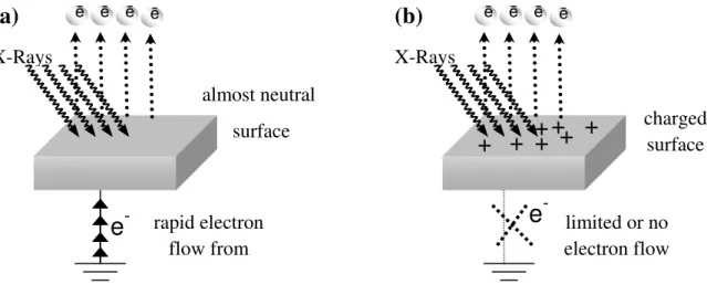
During an XPS measurement, electrons flow from the sample to the electron analyzer. As a consequence, the emission of photoelectrons from the sample may cause a positive uncompensated charge accumulation, which is referred as “surface charging” in the literature. This also causes a binding energy variation in the XPS spectrum, if the sample isn’t grounded or poorly conductive as modeled in Figure 9b, and a number of methods have been developed for charge compensation. On the other hand, if properly utilized, it can be a valuable tool for obtaining extra information about the surface structure of the sample in the nanometer scale.
15
Figure 9. Charging processes in (a) a conductive and (b) a nonconductive material during recording
of XPS data.
1.1.3.1. Controlled Surface Charging
The peak position can be vary due to the presence of internal and external factors such as creation of photoelectrons, size21 and morphology15, 16 of structures, orientation22, 23 of specimens and surrounding electrostatic conditions of the examined atoms are some examples for internal parameters. For external parameters; applying voltage stress, exposing to stray and low-energy electrons23-29 are some examples. These unwanted variations in peak position (or the binding energy shifts) have been tried to be compensated by employing a variety of techniques. A completely neutralized experimental condition during XPS analysis is only an ideal because the charging process is a dynamical one and usually governed by more than one parameter. On the other hand, the charging of the sample under X-Ray radiation can be an advantage if it can be controlled as reported in many previous works.9, 23, 24, 26, 29-33
(b)
X-Rays ē ē ē ēe
-+ -+ -+
+
+
+
limited or no electron flow charged surface+
rapid electron flow from ground(a)
X-Rays ē ē ē ēe
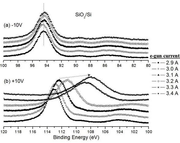
-almost neutral surface16
The positions of photoelectron peaks are equally altered by an applied voltage stress and this can be monitored if the sample is a conductive material (like graphite, see Figure 20); however, the charge accumulation is not only a function of externally applied voltage stress, but is also effected by the charging capacity of the domains. Therefore, locally developed charges create differential shifts even in between two atoms of the same element hosted in different domains of the same sample. In Figure 10b, a special situation is represented; an inhomogeneous charging is developed through a homogeneous and nonconductive SiO2/Si system. In Figure 10a, the SiO2/Si system is subjected -10 V DC stress and e-gun current varies from 2.9 A to 3.3 A while recording XPS data in each step (the experimental set-up is shown in Figure 17). Due to the negative potential on the surface of the SiO2/Si sample, the electrons, mostly originating from the e-gun and also from the X-Ray tube, are almost completely repelled by the intentionally applied negative potential on the surface of sample as modeled in Figure 11a. As a result, an approximately uniform potential is built up and maintained not only on the outmost layers of the SiO2/Si system, but also at least throughout a depth of 10 nm from the surface of the sample (this length corresponds to the probe length of XPS). Therefore the binding energy positions of Si2p(Si+4) peaks do not vary or exhibit any broadening while changing the current level of the e-gun and applying a large enough negative DC stress.
17
Figure 10. The XPS spectra of 2p regions of SiO2/Si sample under (a) -10 V and (b) +10 V DC
stress with varying e-gun currents.
On the other hand, applying an external positive DC stress, +10 V, not only leads to neutralization, but also the sample develops a negative charge since the sample attracts these low-energy electrons now. As a result any variation in the current level of e-gun causes changes in the number of electrons trapped by the sample. In this case Si 2p peaks are not only shifted to lower binding energies, but are also broadened due to an inhomogeneous negative charge accumulation on the surface of the sample as monitored by XPS in Figure 10b and modeled in Figure 11b.
18
Figure 11. Schematic representation of the charging and developed potential of surface structure of
nonconductive SiO2 layer under (a) -10 V and (b) +10 V DC stress with varying the current level of
the low-energy electron flow.
1.1.3.2. Theory and Modeling of Dynamic XPS
The model is based on calculating XPS spectrum of a sample under squarewave or other pulse stresses at different frequencies. In this model the system is considered as a lumped circuit to simplify the steps as illustrated in Figure 12a,34 while the sample is represented by an electrical unit of parallel connected one resistor and one capacitor. The two main currents appear due to photoemission, Ix-ray, and neutralization of the sample with low-energy and stray electrons, Ie-gun. As a result of external voltage source, Vs, varies with
19
time in any waveform fashion (square, sinus, trigonal), surface potential of the sample; Vsurface, also has a dynamic character.
Figure 12. (a) The circuit for the simulation of dynamic XPS system and (b) theoretically
20
To simulate dynamic XPS spectra the lineshape functions are firstly calculated for each frequency within a 10-4-103 Hz range as illustrated in Figure 12b for four different frequencies. At higher frequencies right and left peaks of lineshape function have sharp features and the potential difference between these peaks of the lineshape function is exactly 20 V. However, with decreasing pulse frequency the right and left peaks of lineshape function move towards each other. Therefore, the potential difference between these peaks becomes less than 20 V. In addition the features of right and left peaks of lineshape functions are broadened as shown in Figure 12b. The calculated XPS spectra are obtained by convolution of lineshape functions with a grounded experimental XPS data as illustrated in Figure 13a,b,c. Usually an offset energy is raised in between the binding energy axis of experimentally measured and theoretically calculated XPS spectra as presented in Figure 13c. We are in the process of investigating in detail of this artifact. If offset is corrected from theoretically calculated XPS spectra, an agreement between theoretically calculated and experimental measured spectra is remarkable as shown in Figure 13c as labeled “offset corr.” spectra.
21
Figure 13. (a) Calculated lineshape functions at 1 Hz and 0.001 Hz for an 8.2 MΩ and 1µF
resistance and capacitance values. (b) Grounded XPS spectrum of a graphite sample. (c) Experimentally measured and theoretically calculated XPS spectra of the graphite sample connected with an external RC (8.2 MΩ and 1µF) circuit, and also shown on offset corrected calculated spectra. (d) Schematics diagram of the experiment set-up.
22
Figure 14. Dependence of the calculated peak broadening on squarewave pulse frequency of the
graphite + RC unit sample(dotted line) and measured XPS spectra of C1s of this sample(solid lines) at three different pulse frequencies: 0.001 Hz, 0.018 Hz, and 1 Hz with FWHM values.
In addition, both theoretical and experimental results show that peaks are broadened when the pulse frequency changes from a higher frequency to a lower frequency or vice versa as shown in Figure 14. Peak broadening reaches a maximum point at a specific frequency which is related with resistance and capacitance values of the sample. This figure shows that broadening of C1s peaks of the RC + graphite sample reaches a maximum around 0.018 Hz to 2.8 eV whereas both 0.001 Hz and 1 Hz this value is only 2.1 eV, in agreement with the theoretical results. We prefer to call this frequency, where broadening reaches a maximum value as the “inflection point”.
23
2. AIM OF THE WORK
Previous works on SiOXNY/Si,8, 29 SAMs/SiOX/Si,35, 36 AlYOX/Al and WOX/W,26 GeOx/Ge,37 and SiOX/Si,10, 15, 23, 27, 34, 38-42 systems were extensively investigated by Suzer’s group for better understanding the nature and the mechanism of charging/discharging properties which are important in developing next generation devices.
The technique of applying an external D.C. voltage stress (a static stress) during recording XPS measurements, to accumulate purposely a charge on the insulators, or layers with heterogeneous composition, or domains or multi layers, helps to analyze these composite substances via monitoring the induced shifts in between related peaks. This method can be called as “Charge-Contrast Technique” and does not involve the time as an additional parameter. For incorporation of the time to XPS measurements and for probing dynamic behavior of charging and discharging processes of dielectric materials we have applied squarewave pulses to the sample during recording of XPS data. We refer this “Dynamical XPS” and in this thesis we would like to show that dynamic XPS is an appropriate technique to extract some electrical information (effective resistance and capacitance values) of thin organic layers with also chemical specificity. We have chosen thin polystyrene (PS) and poly(methyl methacrylate) (PMMA) polymeric films (with 15-55 nm thickness) for application of our technique, since it is known that these polymers are not miscible and phase-separate under normal blending conditions.43-51
24
3. EXPERIMENTAL
3.1. Surface Coating
Coated composite materials are attractive subject for their wide technological applications. Polymeric materials are usually preferred as surface coating agents, due to their simplicity in controlling many properties including morphology. Additional functionalities can also be added to them by blending with more than one polymer which has different properties. For this reason, blend polymeric coating agents have been extensively investigated, and reported works show that the surface composition of an immiscible blend film is primarily controlled by the surface free energy of polymers.44-46, 48,
49, 52-56 Other significant parameters which determine surface composition of films are
molecular weight,51, 52, 54, 55, 57-59 end group(s) of polymers54, 60-62, substrate50, 52, 56, solvent,45, 55, concentration45 and relative fractions of blend polymers.49, 52, 53, 55. As a consequence, lateral phase-separated structures at the surface of the films can be developed by casting an immiscible blend polymeric solution from a common solvent. As discussed in the references given above, the phase separation at the surface of thin polymeric films is generally investigated using a number of different techniques like Atomic Force Microscopy (AFM), Sum Frequency Spectroscopy (SF), Attenuated Total Reflection FTIR (ATR-FTIR), and Water Contact Angle (WCA).
Spin coating and dip coating are the simplest polymeric coating techniques. Spin coating technique is based on an excess amount of polymeric solution which is decanted on the substrate and rotated at a desired speed to spread the solution by centrifugal forces, as
25
illustrated Figure 15a,b,c. Rotation of the substrate continues until excess solution is spun off and also the remaining solvent is entirely evaporated from the surface of the substrate to form a solid thin film. Spin coating technique provides uniform thin films even at the nanometer scale.
26
The technique of dip coating includes an immersion step of the substrate in a polymeric solution. The substrate should be covered by the solution to accomplish the coating process. Enough time should be given outside until the drying is complete to obtain a thin solid film on the surface as also shown in Figure 16.
Figure 16. The procedure of dip coating technique.
Both techniques offer different advantages and we used the spin coating technique to prepare our thin and uniform polymeric films since it is easer to control the thickness of the polymeric layer(s), and also a shorter preparation time is needed to complete the coating process.
substrate
polymeric
mixture
27
3.2. Preparation of Thin PS and PMMA Films on Si Wafers
Mostly p-doped silicon wafer, having (100) orientation, was used as substrate. Approximately a 4 mm x 10 mm silicon was cut from a silicon wafer. This silicon substrate is cleaned with acetone, ethanol or methanol and then put in concentrated HF solutions for a total of 1-2 minutes to get rid of the native oxide layer or other possible contaminations. Afterwards the sample was washed with de-ionized water to remove excess HF and then with acetone to remove both water and HF, and dried under N2(gas) flow. This Si wafer was used as the substrate for casting polymeric layers via spin coating technique. 0.2-0.4 % (w/v) of PS and PMMA granules were dissolved in chlorobenzene. Polymeric solutions are kept in an ultrasonic shaker until a complete dissolution and homogenization was reached. An extra washing process was applied to the Si wafer with the solvent of polymeric solution, chlorobenzene, while the Si wafer was rotating at a higher speed in the spin-coater (Laurell WS-400B-6NPP-LITE). Approximately, 150 µL of 0.4 % (w/v) solution of PS or PMMA was ejected on the Si wafer, which was rotated at 1500 rpm. Rotation lasted for 2 minutes to ensure that entire solvent is evaporated from the films. This time is enough to remove chlorobenzene from thin films because there is no sign of Cl peak in the XPS spectra of thin PS and PMMA films. Average thicknesses of thin films were measured using a stylus profilometer (Sloan Dektak 3030ST).
The same Si wafer preparation procedure explained above was also used to cast an PS/PMMA blend thin film on the substrate. The required amount of (0.2-0.4 % (w/v)) PS and PMMA granule was dissolved in the same solvent; chlorobenzene, to obtain a blend polymeric solution, and cast a thin PS/PMMA blend film on the Si wafer.
28
3.3. Instruments and Techniques
3.3.1. Charge-Contrast XPS
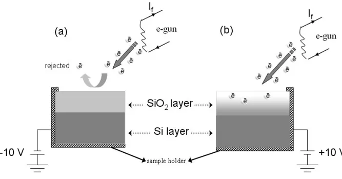
A Kratos ES300 electron spectroscopy with nonmonochromatic Mg Kα X-Rays (at 1253.6 eV) source is employed for recording XPS measurements. The pressure of analysis chamber was kept below 10-8 Torr for the duration of all data recording. The X-rays are directed to the sample with a 450 angle and the electron analyzer is located at the top of the sample with a 900 orientation with respect to the surface of the sample plane, so the take-off angle is 900, unless otherwise mentioned. The sample rod is externally connected to either the ground or a DC power supply or to the squarewave pulse generator to both top and bottom regions of the sample as illustrated in Figure 17.One more power supplies is used to apply a -3.0V potential to the filament and another one to heat the filament. This filament is used as the source of low-energy electrons to neutralize or negatively charge the sample. Stanford Research System DS340 is used as the pulse generator. XPS peaks are fitted and deconvoluted by a third-party free program, XPSPEAK95 version 2.0.63 The binding energy scale of XPS is calibrated according to peak positions of Au 4f (84.0 eV) and Ag 3d (368.3 eV).
3.3.2. Dynamic XPS
As briefly mentioned in the introduction part, instead of applying a DC stress, a square pulse is used to probe dynamically the charging/discharging properties of dielectric layers as shown in Figure 17.
29
Applying pulse to the sample alters time dependent parameters of the sample, both in peak positions and also in peak shapes. If the frequency is very low we approach the case of the DC stress, since the period of the squarewave pulse is so large that the sample has sufficient time to develop the full charge.
Figure 17. The schematic diagram of a typical, DC biased, and dynamic XPS set-up.
Sample
DC
filamentPulse
electron analyzer
Sample
holder
ē
ē
ē ēX-Rays
30
3.3.2.1. The Software for Simulating the Dynamic XPS
A MATLAB® routine is used to calculate the dynamic XPS spectrum at each pulse frequency, which also plots the binding energy difference between the separated peaks against the value of the corresponding pulse frequency for any arbitrarily assigned resistance and capacitance values. The solution is obtained by trying arbitrarily chosen R and C values to reach a good match between theoretically calculated and experimentally measured binding energy differences. This enables us to estimate the effective resistance and capacitance values of various samples.22, 34 In addition, this model provides an opportunity to simulate the broadening of peaks for a varying pulse frequency.
3.3.3. External RC
An electrical unit includes parallel connected resistors and capacitors to each other, which is serially connected to the sample at the outside of analysis chamber. This is employed to mimic the behavior of dielectric materials when applying D.C. and A.C. pulse stresses to a conductive sample.
3.4. Monitoring the Layer Thickness of SiO
2Using XPS and FT-IR
FTIR, Fourier Transform Infrared Spectroscopy, is a commonly used analysis technique for monitoring chemical composition of thin and thick layers on various materials and Si being semitransparent is one of the most examined solids. FTIR is
31
sensitive in 10,000-10 nm range,64 whereas XPS can probe upto only 1-20 nm. However, both techniques overlap in the range of 4-20 nm, therefore we had wanted to compare and combine the information derivable from these two complimentary techniques. For this reason, Si substrates are investigated both by FTIR and XPS. The SiO2/Si systems were prepared by heating the sample at 700 0C in air for different time periods (1.5, 3, 4.5, and 6 hour) to achieve different oxide thicknesses.
Figure 18. (a) The area of FTIR peak of SiO2 layers versus annealing times. (b) The baseline
32
Figure 19. XPS spectra of Si/SiO2 systems with various thicknesses of the SiO2 layers.
The results are shown in Figure 18, where it is seen that the thickness determined by FTIR shows a linear correlation with heating times. Moreover, using FTIR one can detect down to 4 nm of SiO2 layer as illustrated in Figure 18b. Note that this 4 nm layer thickness of SiO2 is confirmed by also XPS as demonstrated in Figure 19. The XPS spectrum of 3 hour heated Si sample has only the Si2p+4 peak which appears around 104 eV, so the thickness of SiO2 layer of this sample is already larger than 10nm as also
33
monitored in Figure 19. However, as we had wanted to demonstrate that the layer thicknesses of SiO2 can be followed by FTIR.
34
4. RESULTS AND DISCUSSIONS
4.1. Applying External DC Voltage Stress to Polymeric Thin Films
As mentioned in the introduction part applying an external bias to a sample while recording XPS data shifts binding energy positions of all peaks because of the variation on the kinetic energy of photoelectrons due to the purposely developed electrical potential on the surface of the sample. Briefly, application of a negative DC bias increases the kinetic energy of photoelectrons because of an additional repelling effect between photoelectrons and the developed negative potential on the surface of the sample. Therefore, according to Equation 2, the binding energy of these photoelectrons would be decreased. It is obvious that the reverse is observed when a positive external bias is applied. In this case an attractive surface reduces the kinetic energy of photoelectrons and their binding energies are measured at higher values as depicted in Figure 20 and same results were reported in earlier works.10, 15, 22, 23, 26-30, 34, 38, 40-42, 65, 66
However, applying negative and positive DC potentials is not expected the same amount of shifts between the same peaks of the same atom hosting in different moieties and domains in the same sample. The reason for this is that the charge accumulation into nonconductive or dielectric materials is varied for each domain according to their charge storage capacities. On the other hand, as illustrated in Figure 20 conductive materials don’t show any presence of charging if a proper ground connection is employed during recording XPS data. Hence the extent of shifts into C1s peaks of graphite is exactly as much as the
35
amplitude of applied DC stress (for both -10 V and +10 V cases) as depicted in the Figure 20.
Figure 20. XPS spectra of C1s regions of a graphite sample connecting to ground, and subjected to
36
Figure 21. C1s region of XPS spectra of thin PMMA film on Si substrate, when the sample is grounded
and under +10 V DC stress both without electron gun, and +10 V DC with 3.0 A current of e-gun, +10 V DC and 3.2 A current of e-gun. +10 V corrections are done by subtracting 10 eV from binding energy axes of spectra. A model of experimental set-up(left) and deconvoluted C1s of envelop PMMA(right) are shown in the insets of Figure.
The electrical properties of a sample greatly relate to molecular structure, consequently altering electrical parameters of the sample during recording XPS data,
37
namely controlling surface charging, presents an opportunity to resolve overlapping peaks and to obtain dielectric and proximity information even for nonuniform composite sample as previously reported by Suzer’s group23, 29, 34 As presented in the Figure 21, the C1s region of XPS spectra of a spin coated thin PMMA film on a Si substrate under different physical conditions is examined with XPS. Both the experimental set-up and deconvoluted C1s envelop of thin PMMA film are given in the inset of Figure 21. The C1s envelop is deconvoluted to three sub-peaks as -C=O, -C-O-, and -C-H considering 1:1:3 intensity ratio to classify the corresponding carbon derivatives via a curve fitting process. First, XPS spectrum of the C1s region of thin PMMA film is recorded while the sample is connected only to ground and e-gun is switched off. In the next step, the sample is subjected to +10 V external DC potential while e-gun is still switched off, and other parameters are kept same with the first case. When a positive external DC potential is applied, the sample attracts stray electrons and neutralization or negative charging occurs even though e-gun is off due to the presence of stray electrons which may originate from the X-Rays tube. In this case, neutralization or negative charge accumulation on PMMA layer is observed as a shift toward to a lower binding energy position for C1s peaks with respect to first case. When e-gun is switched on, and a 3.0 A current is allowed to pass through the filament to generate low-energy electrons, the C1s peak of thin PMMA film is shifted to a further lower binding energy. It indicates that the negative charge accumulation on the PMMA film increases because more electrons are trapped by the sample. To support this claim and to show charge controllability on the surface of the sample by an e-gun, the current of e-gun is increased to 3.2 A and the peak position of C1s shows even further shift to a lower binding energy as compared to the 3.0 A case. While these varied conditions cause successive shifts
38
on the C1s peak position of thin PMMA film, in addition C1s peak broadens because of an inhomogeneous charge which is accumulated on the PMMA layer.
As demonstrated in Figure 21 and 22 spin coated thin PMMA and PS polymeric films on the Si wafer are examined with XPS while the sample is connected to the ground, and subjected to -10 V and +10 V DC stresses. To enhance and elucidate charge storage ability of thin films the e-gun is employed with a fixed amount of current flow (3.0 A unless otherwise noted) on the filament to generate a constant flux of free low-energy electrons to the sample. Figure 22 displays charging behaviors of C1s peaks of both thin PS and PMMA film, and O1s peaks of thin PMMA film with specific conditions as given above. DC stress applied spectra include bias correction by adding and/or subtracting 10 eV from the binding energy axis of -10 V and +10 V applied spectra, respectively, to only bring out the quantity of accumulated charge in each case. In contrast to the graphite example, nonconductive PS and PMMA layers have less than 10 eV shifts in both -10 V and +10 V applied DC stress cases due to a developed positive and negative charge on the surface of the polymeric layers, respectively.
In addition, the shifts related to C1s peaks of thin PS and PMMA films are also different from each other. Under both positive and negative polarity of DC stress the binding energy of C1s peak of thin PMMA film shows a larger shift than thin PS film after the bias correction as shown in Figure 22. Consequently, the PMMA polymeric layer accumulates more both positive and negative charges when compared to the PS polymeric layer under approximately the same conditions. Furthermore, the accumulated charge has an asymmetric manner with respect to the polarity of applied DC stress.
39
Figure 22. (a) After bias correction on XPS spectra of C1s regions of thin PS film, and (b) C1s and
(c) O1s regions of thin PMMA film on a Si wafer while connecting ground, subjecting -10 V, and +10 V DC bias.
Moreover, C1s and O1s peaks of PMMA have almost identical behavior at the same conditions because carbon and oxygen atoms of PMMA polymer are adjacent to each other and their photoelectrons are similarly affected by the locally developed charges (potentials). Therefore, our technique becomes a useful tool to offer additional information about the proximity of moieties or domains to assess if the elements are in same domain or not.
40
Figure 23. (a) XPS spectra of deconvoluted C1s and O1s envelopes of PMMA. (b) The measured
surface charging on each sub-peak of C1s and O1s as a function of the applied external bias in the presence of 3.0 A e-gun current.
Besides, the polarity of DC stress determines the sign of the surface charging on dielectric materials by generating a proper surface potential, it is also governed by the varying e-gun current as depicted in Figure 10b for the SiO2/Si sample under fixed a DC stress. Similarly as shown in Figure 23b charging on the surface of thin PMMA film is also
41
controllable with the amplitude of the DC stress. In addition, it looks like charging responses of each group of C and O atom of PMMA is slightly different from each other as shown in Figure 23b contrary to our expectations67, 68 because adjacent groups or domains in the same molecule must feel the same charge.
4.1.1. Phase Separation of Thin PS/PMMA Blend Film
Spin coating technique offers the production of smooth and uniform structured thin film layers on substrates. However, when a mixture of blended polymer is used, the structure of the thin polymeric film layers may become nonuniform and micro or nano phase separated structures may form on the surface and/or within the bulk of films. This phenomenon is usually related to rapid solvent evaporation during the spin coating process.45, 52, 54, 56, 69 If blended polymers have significantly different solubility in the common solvent, the phase separation on the surface of films is more remarkable. These phase separated structures are frequently characterized by AFM,45, 48-50, 53, 56, 61, 70 Sum-Frequency Spectroscopy,44, 46 and WCA.
As we had seen in the previous section PS and PMMA have significantly different chemical structures, hence they have different charging capacities. As a result, thin PS and PMMA polymeric films display different shifts under DC stresses as demonstrated in Figure 22a,b. Therefore, the immiscible PS/PMMA blended films may also show phase separation during XPS investigation. For this reason, a comparable thickness PS (ca. 20nm), PMMA (ca. 20nm), and 50:50 % by weight PS/PMMA (ca. 15nm) blend films are prepared by casting from a common solvent, chlorobenzene, which is a proper solvent for
42
both PS and PMMA to eliminate solvent effect. Our Charge-Contrast Technique is employed to examine these thin polymeric films. Under the -10 V DC stress as shown in the inset of Figure 24b, the phase separation on the XPS spectrum of PS/PMMA blend film is clearly observed with a spectroscopic technique because different charges are accumulated on each individual domain of PS and/or PMMA. Under the +10 V DC stress case as shown in Figure 24a, similar differential charging may occur on C1s peaks of PS and PMMA domains. However, in this case the C1s envelope of PMMA of PS/PMMA blend film shifts towards the C1s of the PS domain of PS/PMMA blend film, so that C1s regions of PMMA and PS overlap. Therefore, there is no clear and observable peak separation between C1s peaks of PS and PMMA domains on the XPS spectrum of the blend film even though charge difference is possible to develop. However, it is still possible to illustrate charge contrast between them by a further peak fitting and deconvoluting process.
43
Figure 24. The XPS spectra of C1s regions of thin PS, PMMA and blend PS/PMMA films under
(a) +10 V, (b) -10 V DC stress, and (c) grounded without bias correction.
4.2. Applying Square Wave Pulse for Monitoring Frequency
Dependence of Thin Films
While the surface charging can be controlled by applying DC stress, it can also be controlled and enhanced with utilizing a pulsed time varying potential. For example a squarewave pulse stress can be applied to the sample to achieve such a dynamical information to yield resistance, capacitance, and/or time constant value related to the charging and discharging properties of materials.22, 34 The method of subjecting the pulse
44
stress to the sample rod is more favorable to examine dynamic charging/discharging behavior than other methods, for instance, an e-gun system which can be turned on and off or an e-gun system that has a shutter can also be used to control surface charging dynamically. However, turning on and off an e-gun is not well suited, because of the difficulty of directing the free electron towards to the sample and also closing-opening of an e-gun system is not rapid enough to meet our requirements. The employment of squarewave pulse to the sample rod is practical and easily applicable to control the surface charging. In addition, the most is that it is a noncontact technique and capable of analysis of fragile organic layer that is extremely difficult or impossible to reach such a reasonable level of accuracy with conventional electrical measurement methods. Accordingly, the spin coated thin polymeric films of PS, PMMA, and PS/PMMA blends are analyzed with XPS while subjecting squarewave pulses, with ±10 V amplitude and in the 10-3 - 103 Hz frequency range.
45
Figure 25. The C1s region of XPS spectra of (a) graphite, (b) PS(ca. 20 nm) and (c) PMMA(ca. 20
nm) thin films when samples are grounded and subjected to ±10 V squarewave pulses at 1 Hz and 0.001 Hz. The inset shows experimental set-up of the dynamic XPS.
In Figure 25a, C1s region of XPS spectra of the graphite sample is given, when the sample is under 1 Hz and 10-3 Hz squarewave pulse stresses as specified above and also when it is grounded. While applying squarewave pulse, the graphite sample spends half of the total measurement time under -10 V and the other half is spent under +10 V in a cyclic manner, so the C1s peak of graphite splits into two peaks, and each peak is shifted according to the amplitude and the polarity of the pulse stress. Therefore, the split peak at
46
higher binding energy is due to the +10 V cycle of the pulse, and the peak at lower binding energy is due to the -10 V cycle. Both at the higher and lower frequency, the C1s peak of graphite is shifted exactly -10 eV and +10 eV with respect to grounded binding energy position since graphite is a good conductive material. As a result of this binding energy difference is measured as 20 eV at all frequencies as shown in Figure 25a. However, since thin PS and PMMA films are dielectric materials, one measures less than 20 eV binding energy differences at the lower frequency as a consequence of charge accumulation on both PS and PMMA polymeric thin films as demonstrated in Figure 25b,c. In contrast, at high frequencies the binding energy difference between these split C1s peaks of thin PS and PMMA film converges to 20 eV as in the graphite’s case because at higher frequency the sample doesn’t have enough time to charge and discharge. As a consequence, the measured binding energy differences of thin PS and PMMA films exhibit strong frequency dependence.
47
Figure 26. Frequency dependences of measured binding energy difference of thin PS (ca. 20 nm),
PMMA(ca. 20 nm), and immiscible PS/PMMA(ca. 15 nm) blend films.
To monitor the frequency dependences of the measured binding energy difference of 20 nm of PS, 20 nm of PMMA, and 15 nm of an immiscible thin PS/PMMA blend film, the samples are subjected to squarewave pulse stresses at varying frequencies in the range of 10-3-103 Hz. The frequency dependences are depicted in Figure 26. The frequency dependences of PS and PMMA have different appearances, but the frequency dependence of the PS/PMMA blend does not have a uniform feature. In fact it is a hybrid feature of behaviors of thin PS and PMMA films.
48
4.2.1. Extracting Electrical Information of Thin Film via Software
It is interesting that we can measure resistance and the capacitance values of such materials of spin coated thin polymeric films having thicknesses around 15-55 nm from frequency dependence of the corresponding peaks with dynamic XPS and reproducing experimental data faithfully using a simple equivalent electrical model via the developed software program. The model is simple and validation is checked by comparing theoretically calculated and experimentally measured frequency dependence data in published articles22, 34 and also will be reintroduced in the subsequent parts.
4.2.1.1.
Fitting Resistance and Capacitance Values of Thin
Polymer Films
Calculation the model of dynamic XPS spectra at each frequency are carried out and plotted as binding energy difference between the split peak positions versus the corresponding frequency as illustrated in Figure 27a, using a coded program in MATLAB® with arbitrarily assigned resistance and capacitance values. Determination of resistance and capacitance values requires an attempt to try different R and C values until a good agreement between features of the frequency dependence of experimentally measured plot and theoretically calculated one is reached. This gives us an idea of effective approximate resistance and capacitance values of the sample under investigation.22, 34
49
Figure 27. (a) Frequency dependence of the measured binding energy difference of thin PS film
and calculated binding energy differences at same resistance, but with different capacitance values. The arrow shows direction of the increment in the capacitance value. (b) Calculated broadening behaviors corresponding to these resistance and capacitance values. The solid lines are theoretically calculated and the line+symbol are the experimentally measured values plotted in a semilog fashion.
In addition, the program can predict the broadening with a varying resistance and capacitance value as illustration in the Figure 27b, which will be utilized in the next part.