OPEN ACCESS
SbSI Based Photonic Crystal Superlattices: Band
Structure and Optics
To cite this article: Sevket Smsek et al 2015 IOP Conf. Ser.: Mater. Sci. Eng. 77 012020
View the article online for updates and enhancements.
Related content
Electrical and Optical Properties of SbSI Films
T. Sudersena Rao and Abhai Mansingh
-Grain Orientation of SbSI Ceramics
Kazuo Shoji and Yasuo Uehara
-Effective mass of photons and the existence of heavy photons in photonic crystals
V S Gorelik
-Recent citations
Optical study of Sb–S–I glass photonic crystals
Anna Starczewska et al
-SbSI Based Photonic Crystal Superlattices: Band Structure
and Optics
Sevket Sımsek1, Husnu Koc2, Selamı Palaz3, Oral Oltulu3, Amırullah M.
Mamedov4,5 and Ekmel Ozbay4
1 Hakkari University, Faculty of Engineering, Department of Material Science and Engineering, 3000, Hakkari, Turkey
2 Siirt University, Faculty of Science and Letters, Department of Physics, 56000, Siirt, Turkey 3 Harran University, Faculty of Science and Letters, Department of Physics, 63000, Sanliurfa, Turkey
4 Bilkent University, Nanotechnology Research Center, 06800, Ankara, Turkey 5 Baku State University, International Scientific Center, Baku, Azerbaijan E-mail: [email protected]
Abstract. In this work, we present an investigation of the optical properties and band structure
calculations for the photonic crystal structures (PCs) based on one-dimensional (1D)-photonic crystal. Here we use 1D SbSI based layers in air background. We have theoretically calculated the photonic band structure and optical properties of SbSI based PC superlattices. In our simulation, we employed the finite-difference time domain (FDTD) technique and the plane wave expansion method (PWE), which implies the solution of Maxwell equations with centered finite-difference expressions for the space and time derivatives.
Keywords: Fibonacci Photonic Crystal, SbSI, Supercell
1. Introduction
It is well known that the photonic crystal (PC) based superlattices can play an essential role in the controlling of the optical processes in various devices of optoelectronics [1]. Therefore, great attention is paid to the investigation of the physical properties of PC based superlattices. The PC based superlattices of various types are considered, namely, strictly periodic, disordered, lattices with defects, etc. The structures intermediate between the periodic and disordered structures, or quasi-periodic lattices – the Fibonacci and Thue-Morse superlattices, occupy a special place among the superlattices. On the other hand, one of the topics of interest in the optics of PC is the possibility to tailor emittance/absorptance by changing the distribution of electromagnetic modes. Emittance tailoring by conventional PCs was investigated in [2,3]. One of the structures that may be used in emittance tailoring is quasiperiodic multilayers, like the Fibonacci superlattices [4]. Due to their structural self-similarity, these show regularities in their transmission/reflection spectra. The strong resonances in spectral dependences of fractal multilayers can localize light very effectively [1,5]. In addition, long-range ordered aperiodic photonic structures offer a extensive flexibility for the design of optimized light emitting devices, the theoretical understanding of the complex mechanisms governing optical gaps and mode formation in aperiodic structures becomes increasingly more important. The formation of photonic band gaps and the existence of quasi-localized light states have already been demonstrated for one (1D) and two-dimensional (2D) aperiodic structures based on Fibonacci and the Thue-Morse sequences [1,4]. On the other hand, a one – dimensional Schrödinger equation has been examined with a stepwise quasiperiodic potential whose value is equal to either of the two fixed values sequentially in accordance with the Fibonacci set [1]. For such a potential, an electron was found to Content from this work may be used under the terms of theCreative Commons Attribution 3.0 licence. Any further distribution of this work must maintain attribution to the author(s) and the title of the work, journal citation and DOI.
have a “critical wave function” with strong spatial fluctuations. This type of wave function correlates with the properties of the energy spectrum. The unusual electron properties of quasiperiodic potentials have also stimulated extensive research of the optical counterparts. However, to the best of our knowledge, a rigorous investigation of the band gaps and optical properties in the more complex types of aperiodic structures has not been reported so far.
In this paper, we investigated the energy spectrum and optical properties in the Fibonacci-type photonic band gap (PBG) structures consisting of ferroelectric material (SbSI) in detail by using the finite-difference time-domain (FDTD) method and the plane wave expansion method (PWE). The choice of the SbSI crystal as the active media for our investigation was associated with its unusual optical and electronic properties. It is well known, that SBSI is the ferroelectric material and its properties are very sensitive to external influences (temperature, electric field, stress and light) [6-8]. Therefore, SbSI based Fibonacci photonic crystal may be used as efficiency material for photonic devices.
2. Computational Details
2.1. Fibonacci Sequences and Model
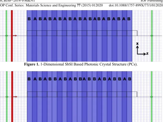
Quasiperiodic structures are nonperiodic structures that are constructed by a simple deterministic generation rule. In a quasiperiodic system two or more incommensurate periods are superimposed, so that it is neither aperiodic nor a random system and therefore can be considered to intermediate the two [1]. In other words due to a long-range order a quasiperiodic system can form forbidden frequency regions called pseudo band gaps similar to the band gaps of a PC and simultaneously possess localized states as in disordered media [5]. The Fibonacci multilayer structure (well-known quasiperiodic structure) has been studied in the past decade, and recently the resonant states at the band edge of the photonic structure in the Fibonacci sequence have also been studied experimentally [9]. A 1D quasi-periodic Fibonacci sequence is based on a recursive relation, which has the form, Sj+1={Sj-1, Sj} for j≫1, with S0={B}, S1={A}, S2={BA}, S3={ABA}, S4={BAABA} and soon, where Sj is a structure obtained after j iterations of the generation rule. Here, A and B are defined as being two dielectric materials, with different refractive indices (nA, nB) and have geometrical layer thickness (dA, dB). In place of materials A and B, we used air (A) and strongly anisotropic material - antimony sulfoiodide (SbSI, B) [10]. In Fig. (1) and (2) we schematically show the geometry of conventional PCs and FPCs. 1D photonic crystals are characterized by the refractive index contrast and filling fraction. The refractive index contrast is the ratio of the higher refractive index to the lower refractive index in the multiplexer system. The filling fraction f is the ratio between the thickness of the lower refractive index layer (air) and the period of the PC, i.e., f=d1/(d1+d2). Typical 1D PCs and FPCs are shown Fig.1 and Fig.2
The thickness of the considered layers of air and SbSI are and
, respectively. The lattice constant is . The filling fraction is set to 0.5. The refractive index contrasts of anisotropic SbSI are taken as following:
na=2.87 nb=3.63 nc=4.55 Tc = 22 ºC (Paraelectric Phase)
na=2.87 nb=3.57 nc=4.44 Tc ≈ 12 ºC (Ferroelectric phase) at λ=633 nm.
Figure 1. 1-Dimensional SbSI Based Photonic Crystal Structure (PCs).
Figure 2. 1-Dimensional SbSI Based Fibonacci Photonic Crystal Structure (FPCs).
2.2. Finite Difference Time Domain (FDTD) Method and Plane Wave Expansion Method (PWE)
In our calculations, we used the OptiFDTD software package [11]. The OptiFDTD software package is based on the finite-difference time-domain (FDTD) method for transmission spectra and the plane wave expansion method (PWE) for photonic band structure. Equi-frequency contour of SbSI based 1D PCs was calculated with MPB free software [12].
The photonic band structures of the proposed PCs were calculated by solving the Maxwell equations. The Maxwell equation in a transparent, time-invariant, source free, and non-magnetic medium can be written in the following form:
Where,
is the space dependent dielectric function is the speed of light in vacuum.
is the magnetic field vector of frequency ω and time dependence .
This equation is sometimes called the Master Equation, and represents a Hermitian eigen-problem, which would not be applicable if the wave equation were derived in terms of the electric field. The Bloch theorem states that, due to infinite periodicity, the magnetic field will take the form:
Where
for all combinations of lattice vectors . Thus, Maxwell equation is given in operator form:
By solving these equations for the irreducible Brillouin zone, we can obtain the photonic band structure.
FDTD algorithm is one of the most appropriate calculation tools [13]. For solving Maxwell's equations depending on the time, FDTD algorithm divides the space and time in a regular grid. Perfect matched layers (PMLs) can be used in the determination of the boundary conditions [14]. In general, the thickness of the PML layer in overall simulation area is equal to a lattice constant. FDTD solves electric and magnetic fields by rating depending on space and time and deploys that rating in different spatial regions by sliding each field component half of a pixel. This procedure is known as Yee grid discretization. Fields in these grids can be classified as TM and TE polarization. In our calculations, we have used Periodic Boundary Condition (PBC) and (PMLs) at x- and z-directions, respectively.
3. Results and Discussion
3.1. Photonic Band Structure and Transmittance
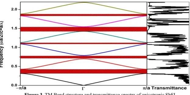
We calculate the spectral properties in the n-th order (n=10) Fibonacci-type quasiperiodic layered structures consisting of compounds. The photonic band structures of 1D SbSI based PCs have been calculated in high-symmetry directions in the first Brillouin. The band structures with transmittance spectrums for SBSI based photonic crystal are shown in Fig. 3. We can see that there exist five fundamental photonic band gaps (PBG) from Fig.3. The width of the fundamental photonic band gaps are (0.313-0.426) (ωa/2πc) for 1th PBG, (0.700-0.788) (ωa/2πc) for 2nd PBG, (1.091-1.133) (ωa/2πc) for 3rd PBG, (1.424-1.544) (ωa/2πc) for 4th PBG and (1.831-1.883) (ωa/2πc) for 5th PBG, respectively. When the frequency of an incident electromagnetic wave drops in these PBGs, the electromagnetic wave will be reflected completely by the photonic crystal. It can be seen in Fig.3 that transmittance is zero in these range of frequencies. All pseudogaps exist in the frequencies where the effective refractive index of the structure are positive and the spectral width of the gaps are invariant with the change in the transmittance (see, Tables 1).
Band Gap (ωa/2π c) Gap Size( %) Band Gap (ωa/2π c) Gap Size( %) Band Gap (ωa/2π c) Gap Size( %) Band Gap (ωa/2π c) Gap Size( %) Band Gap (ωa/2π c) Gap Size( %) 0.1 (0.424-0.499) 16.165 (0.865-0.992) 13.728 (1.326-1.477) 9.099 (1.806-1.944) 7.350 (2.297-2.391) 4.009 0.2 (0.376-0.493) 26.806 (0.811-0.948) 15.544 (1.295-1.343) 3.596 (1.712-1.792) 4.534 (2.123-2.265) 6.437 0.3 (0.346-0.479) 32.128 (0.797-0.860) 7.628 (1.190-1.289) 8.002 (1.600-1.712) 6.791 (2.047-2.089) 2.041 0.4 (0.326-0.455) 33.007 (0.771-0.793) 2.831 (1.111-1.235) 10.541 (1.542-1.588) 2.940 (1.899-2.012) 5.790 0.5 (0.313-0.426) 30.508 (0.700-0.788) 11.815 (1.091-1.133) 3.814 (1.424-1.544) 8.109 (1.831-1.883) 2.830 0.6 (0.304-0.395) 25.887 (0.650-0.764) 16.020 (1.035-1.088) 5.046 (1.387-1.432) 3.160 (1.708-1.819) 6.296 0.7 (0.299-0.365) 19.961 (0.618-0.722) 15.615 (0.959-1.064) 10.282 (1.318-1.381) 4.618 0 0 0.8 (0.296-0.339) 13.454 (0.599-0.676) 11.969 (0.912-1.010) 10.212 (1.234-1.338) 8.020 (1.564-1.658) 5.822 0.9 (0.295-0.315) 6.645 (0.592-0.630) 6.187 (0.889-0.946) 6.182 (1.189-1.260) 5.748 (1.491-1.574) 5.399
Table 2 Variation of full band gap size for TE modes with filling factor for anisotropic SbSI based
layers in air background. Filling
Factor TE1 TE2 TE3 TE4 TE5
Band Gap (ωa/2π c) Gap Size( %) Band Gap (ωa/2π c) Gap Size( %) Band Gap (ωa/2π c) Gap Size( %) Band Gap (ωa/2π c) Gap Size( %) Band Gap (ωa/2π c) Gap Size( %) 0.1 (0.401-0.498) 21.633 (0.829-0.990) 17.704 (1.287-1.466) 13.036 (1.769-1.916) 7.976 (2.263-2.336) 3.156 0.2 (0.346-0.490) 34.383 (0.775-0.925) 17.704 (1.262-1.279) 1.301 (1.622-1.754) 7.810 (2.041-2.196) 7.304 0.3 (0.314-0.471) 39.805 (0.763-0.810) 5.927 (1.109-1.248) 11.815 (1.528-1.619) 5.767 (1.911-2.018) 5.487 0.4 (0.293-0.439) 39.621 (0.708-0.761) 7.180 (1.037-1.161) 11.268 (1.419-1.518) 6.710 (1.790-1.876) 4.653 0.5 (0.280-0.402) 35.689 (0.634-0.748) 16.476 (1.024-1.038) 1.355 (1.311-1.437) 9.144 (1.672-1.776) 6.040 0.6 (0.271-0.366) 29.720 (0.584-0.713) 19.801 (0.935-1.018) 8.539 (1.289-1.301) 0.931 (1.563-1.667) 6.412 0.7 (0.266-0.334) 22.620 (0.552-0.662) 18.221 (0.860-0.979) 12.942 (1.184-1.275) 7.329 (1.517-1.549) 2.075 0.8 (0.263-0.306) 15.114 (0.534-0.612) 13.593 (0.813-0.915) 11.802 (1.102-1.214) 9.646 (1.398-1.507) 7.516 0.9 (0.262-0.282) 7.421 (0.526-0.564) 6.990 (0.791-0.848) 6.934 (1.058-1.129) 6.492 (1.327-1.411) 6.129
Table 1 Variation of full band gap size for TM modes with filling factor for anisotropic SbSI based
layers in air background. Filling
Factor TM1 TM2 TM3 TM4 TM5
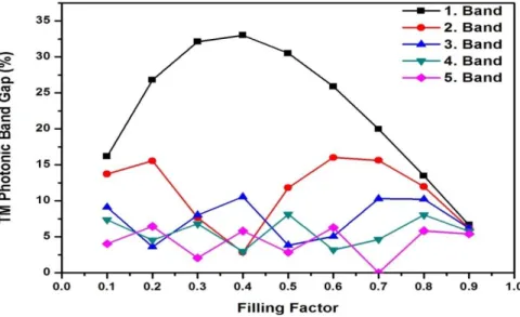
The numerical results of the variation of a full band gap with a changing filling factor from 0.1 to 0.9 are given in Table 1 and Table 2. The variation of band gap sizes (%) as a function of filling factor are shown for TM mode in Fig. 4. It is clear that the size of the gap increases with filling factor for the first band gap. The largest gap size is about 38% when filling factor is as high as 0.4, but it decrease when filling factor continues to increase. On the other hand, the fifth band gap size does not change too much according to filling factor, but it reaches the minimum value when filling factor is 0.7. We also calculated the field distribution of the TM modes in our n-th (7) order Fibonacci sample, following a standard PWE method. The magnitude of the magnetic field (E) at the left interface of the dielectric layer is simply related to H at the right interface of the same layer by using matrix relation [15]. For 1D structures, it is also possible to compute the magnetic field distribution inside the sample (Fig. 5). The insets show the normalized field intensity distribution for the λ=1.55 μm wavelength on the n-th (n=7) interface.
Figure 4. TM Filling factor for anisotropic SbSI.
Figure 6. TM Transmittance spectra of 1D SbSI based PCs.
Figure 7. TM Transmittance spectra of 1D SbSI based FPCs.
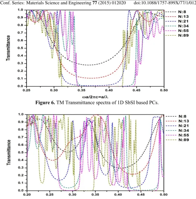
Figs. 6-7 show the transmittance spectra of SbSI based both normal PCs and FPCs from 8 to 89 layers for the transverse-magnetic (TM)-polarized incident electromagnetic wave. The positions of the minima in the transmission spectrum correlate with the gaps obtained in the calculation. A transmission spectrum of a simple eight-layer (also n=8, 13, 21, 34, 55, 89) 1D SbSI based PC is compared in Fig. 6-7 with an eight-layer (also n=8, 13, 21, 34, 55, 89) 1 D SbSI based FPC. One full period in spectrum is presented which corresponds to the frequency range (0.2-0.5) (ωa/2πc). Although there is still a gap in the transmission spectrum of the Fibonacci structure around (0.2-0.5) (ωa/2πc) the spectrum modified significantly. Notably, the total number of transmission peaks in both cases equal to the total number of elementary layers in the structure. This is general property of multilayer structures. In addition, the spectral regularities inherent in Fibonacci structures have also been derived in analytical form based on the transfer matrix approach. Fibonacci structures feature a transmission band in the center which first splits into two and then into three subbands (Fig. 7). This central triplet is indicative for the Cantor triadic set and for higher generations definite self-similar and scaling features develop that are inherent in fractals. Different portions of transmission spectra for the same high-order generation of Fibonacci structure do exhibit similar spectral shape which becomes apparent when using the “exciton in quantum dot” lowest state energy expansion [1]. The transmission spectra of Fibonacci structures also show scalability which means that the spectra of different generations have a similar shape when the frequency axis is properly scaled. Notably, the transmission
peaks have a transmission coefficient close to unity.
3.2. Equi-frequency surface
Because, the momentum conservation law is satisfied at the reflection and refraction of waves, it is convenient to analyze the reflection and refraction of a certain wave in the space of wave numbers
by introducing the equi-frequency surface of the wave. This surface is directly described by the dispersion relation of the anisotropic medium at the fixed frequency ω. Then, the group velocity of the wave in an anisotropic medium can be found as the frequency gradient in the space of wave vectors [16]. It is known that for an electromagnetic wave propagating in an anisotropic medium with a fixed frequency ω, the equi-frequency surface represents a sphere. In this case, the wave vector and group velocity vector , which determines the ray direction, are always parallel. However, equi-frequency surface is not spherical for anisotropic media and the vectors and are not parallel. By analogy with 3D case, the propagation, reflection, and refraction of the wave in 2D structure can be described in terms of the equi-frequency dependence which can be considered as the
section of the dispersion surface in the space of variables by the plane
corresponding to constant frequency. It is well known that the analysis of equi-frequency dependences is most efficient in the studies of 2D geometries, especially in solving problems when only orientations of the and vector of incident, reflected, and refracted waves are of interest, and are not the amplitudes of the reflected and refracted rays. The equi-frequency dependence has a simple physical meaning for the analysis of 2D geometries: since this dependence describe all the possible waves with the given frequency ω and various wave vectors, the directions of the reflected and the refracted rays can be determined by simply finding the points in equi-frequency dependences of media that satisfy the momentum conservation law at a known orientation of the boundary and a given angle of incidence of the wave. Now, we present some numerical examples for our PC structures. In all of these examples, we exploit symmetry to calculate the equi-frequency surfaces over the irreducible Brillouin Zone of the entire Brillouin Zone. First, we consider the equi-frequency surface of a square lattice of SbSI based dielectric layers in an air medium for the –polarization.
Here, the map was discretized using six field points per edge of the unit cell for the first band in Figure 8 (a). The map was discretized using four field points per edge of the unit cell for the second band. The curves shown correspond to equi-frequency surfaces of the lowest order band up to frequencies just below the band gap starting at around 0.11 (2πc/a). For the second band, the curves shown correspond to equi-frequency surfaces of the lowest order band up to frequencies just below the band starting at around 0.16 (2πc/a).
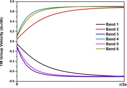
3.3. Group velocity
We believe that a pulse of light propagating along the PC let the pulse be finite in dimension along the direction of propagation. Theoretically, such a pulse can be represented as a wave packet formed as a superposition of the modes, but with a different propagation constant [17]. From [17], it follows that the envelope of the wave packet propagates with the velocity , where is propagation constant. The direct calculation of the derivative of the dispersion relation calculated numerically is not always convenient and can give an error. As shown in [18], the group velocity of the wave packet , is equal to the velocity of energy transfer by the mode . Thus, by using the results of [19] the group velocity can always be calculated with more accuracy, irrespective of the number of points in the dispersion curve. Fig. 9 show the results of calculations of the group velocity of the wave packet formed of the differently polarized localized modes in PC with SbSI dielectirc layers in an air background in 1D.
From Fig. 9, it is evident that the components of the group velocity versus the high symmetry direction (0- ) vary over wide limits. The dependences , which describe the wave packets of localized modes of any polarization and any order, exhibit (generally) a maximum at certain propagation constants. This means that the dispersion of group velocity can be positive, negative, or zero [19]. Therefore, as can be seen in Figure 9, the group velocity of TE-polarized wave packets is almost always higher than that of the TM-polarized packets.
Figure 9. TM Group velocity of anisotropic SbSI. 4. Conclusion
In the present paper the photonic band structures and transmission properties of the 1D SbSI PCs consisting of dielectric layers immersed in air were studied for the first time. We have investigated transmittance spectra of SbSI based both normal PCs and FPCs from 8 to 89 layers. The results show that the number of the repetition period also has a great influence on the average transmittance of the pass band of the both normal PCs and FPCs.
Acknowledgements This work is supported by the projects DPT-HAMIT, DPT-FOTON, and
NATO-SET-193 as well as TUBITAK under the project nos., 113E331, 109A015, and 109E301. One of the authors (Ekmel Ozbay) also acknowledges partial support from the Turkish Academy of Sciences.
References
[1] S V Gaponenko 2010 Introduction to Nanophotonics Cambridge University Press N.Y p.485 9
[2] M Maksimovic, Z Jaksic 2006 Emittance and absorptance tailoring by negative refractive index metamaterial-based Cantor multilayers J. Optics A: Pure & Appl. Opt. 8 355-362
[3] A N Poddubny, E L Ivchenko 2010 Photonic quasicrystalline and aperiodic structures Physica E
42 1871 – 1895
[4] A Rostami, S Matloub 2005 Exactly solvable inhomogeneous Fibonacci-class quasi-periodic structures (optical filtering) Optics Comm. 247 247-256
[5] H Rahimi, A Namdar, S R Entezar, H Tajalli 2010 Photonic transmission spectra in one-dimensional Fibonacci multilayer structures containing single-negative metamaterials Progress In Electromagnetics Research 102 15-30
[6] V M Fridkin 1980 Ferroelectric Semiconductors. New York Consultants Bureau p.314
[7] H Akkus, A M Mamedov 2007Linear and Nonlinear Optical Properties of SbSI: First-Principle Calculation, Ferroelectrics 352 148-152
[8] A K Zeinally, A M Mamedov and Sh M Efendiev 1973 A study of SbSI absorption edge, Ferroelectrics 6 119–122
[9] L Dal Negro, C J Oton, Z Gaburro, L Pavesi, P Johnson, A Lagendijk, R Righini, M Colossi, D S Wiersma 2003 Light Transport through the Band-Edge States of Fibonacci Quasicrystals Phys. Rev. Lett. 90 055501-055505
[10] D Lusk, I Abdulhalim, F Placido 2001 Omnidirectional reflection from Fibonacci quasi-periodic one-dimensional photonic crystal Optics Comm. 198 273-279
[11] OptiFDTD 10, http://www.optiwave.com/.
[12] S G Johnson, J D Joannopoulos, The MIT Photonic-Bands Package (http://ab-initio.mitedu/mpb/).
[13] A Taflove and S C Hagness 2000 Computational Electrodynamics: The Finite-Difference Time-Domain Method 2nd ed., MA: Artech House Publishers, Boston.
[14] J P Berenger 1994 A perfectly matched layer for the absorption of electromagnetic waves J. Comput. Phys. 114 185–200
[15] F L Pedrotti, L S Pedrotti 1987 Introduction to Optics Pretice- Hall Englewood Cliffs NJ
[16] E H Lock 2008 The properties of isofrequency dependences and the laws of geometrical optics, Physics-Uspekhi 51(4) 375-393
[17] A S Spitsyn and G F Glinskii 2008 Properties of Waveguide Modes in a Photon Crystal Based on Slotted Silicon with a Defect Semiconductors 42(10) 1237-1243
[18] A Yariv, P Yeh 2007 Photonics: Optical Electronics in Modern Communications Oxford University Press USA.
[19] A V Kildishev, V M Shalaev 2011 Transformation optics and metamaterials Physics-Uspekhi