Grating based plasmonic band gap cavities
S. Seckin Senlik, Askin Kocabas, and Atilla AydinliTurk Telekom Laboratory, Department of Physics, Bilkent University, Ankara, 06800, Turkey *[email protected]
Abstract: We report on a comparative study of grating based plasmonic band gap cavities. Numerically, we calculate the quality factors of the cavities based on three types of grating surfaces; uniform, biharmonic and Moiré surfaces. We show that for biharmonic band gap cavities, the radiation loss can be suppressed by removing the additional grating component in the cavity region. Due to the gradual change of the surface profile in the cavity region, Moiré type surfaces support cavity modes with higher quality factors. Experimentally, we demonstrate the existence of plasmonic cavities based on uniform gratings. Effective index perturbation and cavity geometries are obtained by additional dielectric loading. Quality factor of 85 is obtained from the measured band structure of the cavity. ©2009 Optical Society of America
OCIS codes: (240.6680) Surface plasmon; (350.2770) Gratings; (140.3948) Microcavity devices.
References and links
1. W. L. Barnes, A. Dereux, and T. W. Ebbesen, “Surface plasmon subwavelength optics,” Nature 424(6950), 824– 830 (2003).
2. M. Moskovits, “Surface-Enhanced Spectroscopy,” Rev. Mod. Phys. 57(3), 783–826 (1985).
3. J. S. Biteen, L. A. Sweatlock, H. Mertens, N. S. Lewis, A. Polman, and H. A. Atwater, “Plasmon-enhanced photoluminescence of silicon quantum dots: Simulation and experiment,” J. Phys. Chem. C 111(36), 13372– 13377 (2007).
4. Y. Gong, J. Lu, S.-L. Cheng, Y. Nishi, and J. Vučković, “Plasmonic enhancement of emission from Si-nanocrystals,” Appl. Phys. Lett. 94(1), 013106 (2009).
5. S. A. Maier, P. G. Kik, and H. A. Atwater, “Optical pulse propagation in metal nanoparticle chain waveguides,” Phys. Rev. B 67(20), 205402 (2003).
6. A. Kocabas, G. Ertas, S. S. Senlik, and A. Aydinli, “Plasmonic band gap structures for surface-enhanced Raman scattering,” Opt. Express 16(17), 12469–12477 (2008).
7. M. Derouard, J. Hazart, G. Lérondel, R. Bachelot, P. M. Adam, and P. Royer, “Polarization-sensitive printing of surface plasmon interferences,” Opt. Express 15(7), 4238–4246 (2007).
8. Y. Y. Gong, and J. Vuckovic, “Design of plasmon cavities for solid-state cavity quantum electrodynamics applications,” Appl. Phys. Lett. 90(3), 033113 (2007).
9. J.-C. Weeber, A. Bouhelier, G. Colas des Francs, L. Markey, and A. Dereux, “Submicrometer in-plane integrated surface plasmon cavities,” Nano Lett. 7(5), 1352–1359 (2007).
10. A. Kocabas, S. S. Senlik, and A. Aydinli, “Plasmonic band gap cavities on biharmonic gratings,” Phys. Rev. B 77(19), 195130 (2008).
11. A. Kocabas, S. S. Senlik, and A. Aydinli, “Slowing down surface plasmons on a moiré surface,” Phys. Rev. Lett. 102(6), 063901 (2009).
12. W. L. Barnes, T. W. Preist, S. C. Kitson, and J. R. Sambles, “Physical origin of photonic energy gaps in the propagation of surface plasmons on gratings,” Phys. Rev. B 54(9), 6227–6244 (1996).
13. A. Kocabas, and A. Aydinli, “Polymeric waveguide Bragg grating filter using soft lithography,” Opt. Express 14(22), 10228–10232 (2006).
14. R. C. Alferness, C. H. Joyner, M. D. Divino, M. J. R. Martyak, and L. L. Buhl, “Narrow-Band Grating Resonator Filters in Ingaasp/Inp Wave-Guides,” Appl. Phys. Lett. 49(3), 125–127 (1986).
15. FDTD Solutions, Lumerical Inc. Suite 201,1290 Homer St.Vancouver, B.C,Canada V6B 2Y5. 1. Introduction
The study of surface plasmon polaritons (SPPs) has been accelerated with the prospect of applications in many areas of science and technology [1]. Localized SPPs associated with metallic nanoparticles have been shown to cause surface enhanced Raman scattering
attributed to high local electric field intensities [2]. Due to high sensitivity of SPP resonances to changes in the effective index, propagating SPPs are already playing a significant role in the detection of low level biochemical species. They may also play an important role in increasing the efficiency of emission from nanocrystals where they are expected to increase light conversion both in light emitting diodes as well as in solar cells [3,4]. Metallic nanoparticles arranged into chain-like waveguide structures are suggested for applications in the area of optical waveguiding for telecommunications [5].
On the other hand, it is well known that metallic periodic structures exhibit modified transmission and reflection spectra owing to the interaction of propagating SPPs with the periodicity. Many features of these SPPs that are excited on periodic metallic surfaces have been studied. Surface enhancement of Raman scattering and photoluminescence signals have already been observed on such structures [6]. In contrast with localized SPPs on nanoparticles, propagating SPPs on periodic surfaces are also being studied for nanolithography and nanophotonic applications [7]. Recently, plasmonic cavities that use Bragg reflectors and selective dielectric loading have been under study [8–10]. In addition to uniform gratings, biharmonic gratings and Moiré surfaces can be used to construct cavity structures. Such cavities can localize plasmons and can lead to small group velocities around the band edges. While they all localize the plasmons, they exhibit different characteristics due to the difference in their design and the mechanism of confinement.
On the other hand, metallic loss at visible wavelengths is a serious problem that hinders the use of plasmons for applications that require long propagation lengths and plasmonic lifetimes. Due, mainly to the same reason, current cavities are characterized by relatively low quality factors that need to be increased to meet expectations. Large quality factors for localized SPPs in cavities then, are crucial for many applications. A cavity designed for localization of SPPs with high quality factors can be used to selectively enhance and suppress spontaneous emission rates of emitters and may provide an ideal platform for cavity quantum electrodynamics (QED). SPP cavities that are expected to work in the strong coupling regime with large enhancements of the Purcell factor have been suggested. Quality factors as high as 1000 have been proposed [8]. Bragg mirrors used in so many photonic structures have been suggested for simple confinement in one dimension and have been shown to exhibit enhanced Purcell factors for applications in cavity QED. Such mirrors have also been employed for SPP localization and characterized with scanning near field optical microscopy to map the electric field distribution in and out of the cavity. Results confirm the cavity formation and localization of the SPP modes [9]. Alternatively, using double exposure interference lithography, biharmonic gratings have been employed to localize SPPs. The quality factor of the demonstrated plasmonic cavity was 37 due to metallic and scattering losses in the cavity [10]. Furthermore and very recently, Moiré surfaces have been demonstrated to support SPP localization at the nodes of a metallic Moiré surface. Smooth variation of the surface relief amplitude in these structures reduces radiative losses leading to relatively higher quality factors (Q=103) [11]. The increased quality factor is promising and suggests further study.
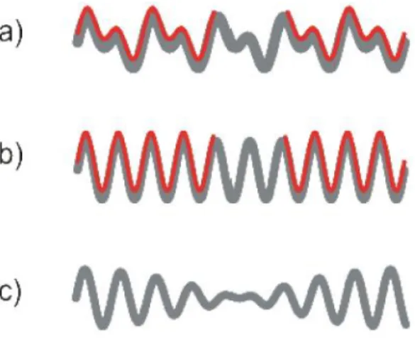
Fig. 1. Surface profile of a) biharmonic, b) uniform and c) Moiré gratings. Note the selectively coated dielectric (red line) on the biharmonic and uniform gratings and the cavity region. Localization takes places around the node of the Moiré surface.
In this work, we study and compare the SPP localization characteristics of uniform, biharmonic gratings and Moiré surfaces. Figure 1 is a schematic description of these cavity types. Experimentally, we demonstrate plasmonic cavity formation on uniform metallic gratings, which consists of a single periodic surface as shown in Fig. 1b. Exploiting the sensitivity of surface plasmons to the effective index experienced by SPPs, localization on uniform gratings have been achieved by selectively coating the metallic surface with silicon. To couple light to the surface plasmons, Kretchman configuration is used to overcome the momentum mismatch between surface plasmons and incoming light. The band gap is provided by the uniform metallic grating while the prism allows for the SPP excitation [12].
The characteristics of the Q factor of plasmonic cavities on uniform, biharmonic gratings and Moiré surfaces are studied numerically. The biharmonic grating, as shown in Fig. 1a, consists of two periodic surfaces with periodicities, such that Λ1=2Λ2. SPP excitation and band gap formation are achieved by using the grating components. The plasmonic cavity mode is obtained through selective loading of the metallic surface. Numerical results clearly indicate that as the amplitude of the larger component is increased the quality factor decreases.
The Moiré surface which is a superposition of two periodic surfaces with slightly different periodicities as shown in Fig. 1c can also support plasmonic cavities. The phase shift at the nodes of the surface leads to localization of the SPPs. The slowly varying grating amplitude around the cavities results in higher quality factors. Moiré surfaces with different periodicities are studied to compare quality factors.
2. Experiment
Fabrication of a uniform grating was achieved with an interference lithography setup. First, we spin a photosensitive polymer (S1800) on 170 µm thick microscope lamella and bake the photosensitive polymer at 110 °C for 1 min. A He-Cd laser operating at 325 nm was used to record periodic structures on the photosensitive polymer using Lloyd’s mirror configuration. Once the structures were developed, they were transferred onto a photocurable polymer (OG146) using the nanoimprint technique [13]. Biharmonic gratings and Moiré surfaces require double exposure of the periods. A 50 nm thick silver film was evaporated on the OG146 polymer to support the surface plasmons. The lamella was then mounted on the base of the prism with the metallic side up. Index matching fluid was used between the prism and the lamella. The BK7 prism allows incoming photons to couple to plasmons. The coupling condition is satisfied at a specific wavelength and angle of incidence. This condition is given by
0 0sin( )
SPP EFF p
k n k n k (1)
where kspp and neff are the wavenumber and the effective index of the SPP’s. k0, α and np are the free space wavenumber of incident photon, angle of incidence and refractive index of the prism, respectively. The dispersion curves of SPP’s are constructed by measuring the coupling wavelength or the angle. We used a spectroscopic ellipsometer (VWASE32) for precise reflectivity measurements. The reflection measurements at different angles of incidences can be used to generate two dimensional reflectivity maps. In order to construct the band structure with high resolution, we scanned the 500-750 nm wavelength range at various angles of incidence, 0.2° apart.
3. Results
3.1 Uniform plasmonic band gap cavities
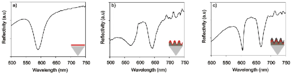
In Fig. 2, wavelength dependent reflection spectra of three different structures are shown with the corresponding experimental configurations. Figure 2a shows the reflection spectra of the TM polarized light from a flat metal surface. As expected, plasmon resonance at the wavelength of 580 nm is observed. However, periodic structure on the surface modifies the dispersion relation. This modification is manifested in the reflection spectrum of a uniform grating and is shown in Fig. 2b. Propagating SPP’s interact with the grooves of the grating and are backscattered. This leads to the formation of standing SPP waves on the uniform grating. Symmetry suggests the presence of two standing waves, labeled λ - and λ+, with two different energies. One localizes on the peaks and the other on the troughs of the periodic structure [12]. A band gap is opened up due to the energy difference between λ - and λ+ modes. The gap is located approximately at 600 nm with the band edges observed at 560 and 635 nm. The width of the band is 23 nm. When the uniform metallic grating is coated with a thin layer of silicon, the effective index experienced by the SPP modes increases which opens up the band gap. The reflectivity spectra of the uniform metallic grating coated with 10 nm of silicon is shown in Fig. 2c.
Fig. 2. Reflectivity spectra of a) flat metallic surface, b) uniform metallic grating with period of 298 nm, c) same uniform metallic grating coated with 10 nm of silicon.
Red shift of the spectrum and opening up of the band gap are clearly observed. The red shift is due to the silicon induced effective index change, experienced by the propagating SPP modes. The widening of the band gap comes from different confinement properties of λ - and λ+ modes on the grating surfaces. The low frequency mode is confined closer to the surface of the samples while the higher frequency component has a longer evanescent tail [12]. Thus, their sensitivity to silicon loading is also different. This allows one to effectively tune the SPP band gap width and position by adjusting the thickness of the dielectric layer. A series of experiments with uniform metallic gratings coated with different silicon thickness were performed and the reflectivity of each sample was measured. The position and width of the band gaps were determined. Effective index of the structure was calculated at the center of the band gap, since neff= np sin(α).
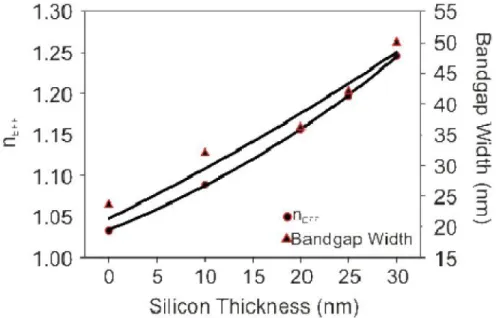
Fig. 3. Effective index and width of the band gap of a uniform grating as a function of silicon loading. The solid lines are to guide the eye.
The increase in neff causes significant changes in the coupling conditions. Larger angle of incidences for incoming photons are needed to compensate for the momentum mismatch in the silicon loaded case. We summarize the results in Fig. 3. The effective index of SPPs can be seen to tune from neff=1.0328 to neff=1.2460 due to silicon loading and the width of band gap is observed to change from 23.0 nm to 50.0 nm.
We construct the band structure for both the uniform metallic grating and that of the dielectric loaded grating from the reflectivity data. The center of the band gap is at 603.0 nm and the width of the band gap is 23.0 nm for the metallic grating. The coupling angle indicates an effective index of neff =1.0328. The center of the band gap is shifted to 715.0 nm and the width increased to 50.0 nm when the sample is coated with silicon. The coupling angle also changes to satisfy the resonance condition. neff becomes 1.2460 at 55.0° in this case.
Considering that the band gap occurs due to destructive interference between forward and backward propagating SPPs in the uniform metallic grating, constructive interference at a specific wavelength in the band gap can also be attained by tuning the relative phases of the propagating waves. Local perturbation of the effective index can lead to these phase changes and enable a localized state in the band gap, called the cavity mode. Having already demonstrated the ability to control the effective index, we design a SPP cavity for the wavelengths in the band gap, using the resonance condition [14]:
(2 1) 4
L n m (2)
where L is the length of the cavity, ∆n is the effective index difference and λ the central wavelength in the band gap.
We start the fabrication of the cavity by photolithographically defining the cavity geometry on the uniform metallic grating. The sample has a number of cavities with the same geometry separated by 10 micrometers in an area of 10x10 mm2. A silicon layer with a nominal thickness of 18.0 nm was deposited on the metallic surface outside the cavity regions. The effective refractive index of SPPs for silicon-coated and uncoated regions of the metallic grating are determined to be n0=1.0328 and n1=1.1445, width of the band gaps are
23.0 nm and 34 nm respectively. High resolution reflectivity spectra of these samples were measured as a function of the angle of incidence. The results are shown in Fig. 4. To clarify cavity formation, we constructed band diagrams of uniform gratings with the cavity. The observed band structure without the cavity is modified with the inclusion of a cavity state in the middle of the band gap, Fig. 4b. This is the consequence of an additional absorption peak observed in the reflection spectrum of the cavity, Fig. 4b. We observe the cavity mode at 655.0 nm for 4.40 µm cavity length where m=1. The Q factor is calculated as 85 while the full-width-at-half-maximum of the absorption peak is 7.7 nm.
Fig. 4. Reflectivity spectra a) and band structure b) of uniform metallic grating with the cavity structure, Note the cavity state (arrow), in the band gap, localized due to selective loading of the uniform metallic grating.
Numerical simulations can shed significant light on various properties of plasmonic structures. We have employed the FDTD Solutions software package by Lumerical [15] to examine the effect the cavity structure on the Q factor, as well as on bandgap width and effective index. The program uses finite difference time domain technique to obtain optical characteristics of the structure. We have used nonuniform mesh around the metal-dielectric interfaces. λ/10 mesh size is used for uniformly meshed parts of the simulation area and 2.0 nm mesh size is used for the nonuniform meshing area. The surface plasmon polariton mode is excited at the metal-air interface which propagates through the structure of interest.
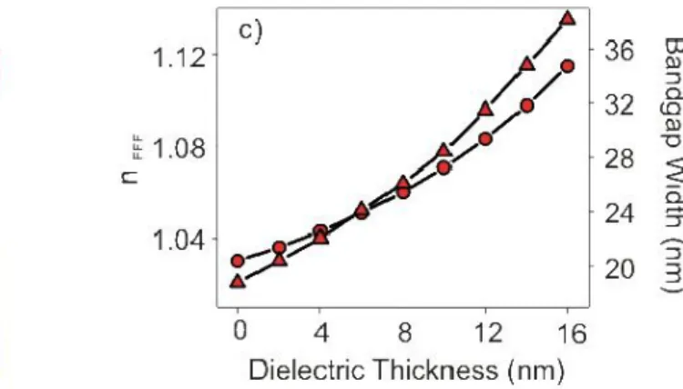
A grating with a modulation depth of 20.0 nm and periodicity of 290.0 nm was chosen. Varying the thickness of the deposited dielectric with refractive index of 2.4 on the grating structure, we studied the effective index and the band gap width. The SPP effective mode index increased from 1.0301 to 1.1149 as the dielectric thickness was increased to 18 nm. Similarly, the band gap width is also increased from 18.7 nm to 38.1 nm. This behavior is summarized in Fig. 5c and is consistent with the experimental results shown in Fig. 2. Selectively loaded cavity geometry on the grating structure was studied under resonance as introduced in Eq. (1). The expected minima in the band gap region, where normally no SPP excitation is allowed, was observed at 652.0 nm for a cavity length of 2.4 µm where m=0 with a dielectric thickness of 14.0 nm. The small difference between the expected cavity length of 2.2 µm and the observed cavity length of 2.4 µm, is due to differences between effective indices of SPP’s on corrugated and flat surfaces, since we calculate the effective indices for a flat surface but measure it on the cavity geometry of the grating surface. The field profile of the cavity mode is illustrated in Fig. 5b. The localization of the field inside the cavity is clearly seen. The electric field distribution is slightly asymmetric since the excitation was done from one side of the structure.
Fig. 5. a) Schematic of the plasmonic cavity structure, b) FDTD simulation of the electric field distribution in a cavity showing the localization of the cavity mode, c) Dielectric dependence of effective index and the bandgap width.
3.2 Biharmonic plasmonic band gap cavities
Biharmonic gratings consist of two uniform gratings with different periodicities. The grating periods are chosen such that Λ1=2Λ2 where Λ1 is used to couple SPP, Λ2 is used to form plasmonic band gaps. The biharmonic geometry can also be recorded on photoresist using interference lithography. After the grating is developed, it is transferred onto a polymer (OG146) and a 50.0 nm metallic thin film is evaporated on the surface to create the metallic surface. These structures have been shown to support plasmonic band gaps and plasmonic cavities through selective loading of dielectrics, by the authors [10]. We have then argued that the grating component which has larger periodicity can lead to radiative losses causing a low quality factor. Our analysis suggested that reducing the grating amplitude can lead to an increase in the quality factor. In order to verify these proposals, we have studied the properties of the biharmonic gratings with FDTD simulations. In the simulation, we construct a biharmonic grating with periodicities Λ1=580 nm with a modulation depth of 20.0 nm and Λ2=290 nm with a modulation depth of 20 nm. The structure under study is depicted in Fig. 6a. A clear cavity mode in the band gap is observed as expected and the associated electric field intensity in the cavity is shown in Fig. 6b.
Fig. 6. The surface profile, a) field distribution, b) and the grating depth dependence of the Q factor for a biharmonic grating, c).
The confinement characteristics of the biharmonic cavity are summarized in Fig. 6. In addition to the field distribution in Fig. 6b, we show the variation of the Q factor with the amplitude of the larger period, Fig. 6c. As we increase the amplitude of this component from 0.0 nm to 40.0 nm, we observe a decrease in the quality factor from 70.0 to 40.0. This is most likely due to out-of-plane radiative losses caused by this additional grating component. This idea is supported by the quality factors observed on uniform gratings reported above.
3.3 Moiré surfaces
Moire surfaces are geometries that consist of two gratings with slightly different periods. It has been shown that Moiré surfaces can also support plasmonic cavities. There are π phase shifts at the nodes of the Moiré surfaces that lead to SPP localization. Experimentally, we have shown that these surfaces support slow surface plasmons [11]. Here, we show the results of the simulation of the cavity state on the Moire surfaces. A Moiré surface consisting of a grating period of Λ1=317.2 nm with a modulation depth of 10.0 nm and a grating period of Λ2=325.0 nm was chosen. The Moiré surface can also be expressed as a superposition of a uniform grating and an envelope function which generates a superperiodicity, D, which is representative of the surface profile. The final Moire surface can be represented by
( ) cos( ) sin( ) S x Gx gx (3) Where 1 2 1 2 2 2 2 , 2 2 2 2 g G d D
. d and D are the uniform periodicity and the
periodicity of the superstructure (half the periodicity of the envelope function). Thus, the expression of the quality factor in terms of superperiodicity reveals the effects of surface profile on Q factor. We observe a cavity mode at 656 nm with a quality factor of 112 on a Moiré surface with d=321 nm and D=13.6. The electric field distribution can be seen in Fig. 7b. In this regime, slow variation of the grating amplitude leads to high quality factors. As we decrease the superperiodicity, the coupling of cavities increases and the quality factor decreases. We have studied Moiré surfaces with different superperiodicities and observe a decrease in the quality factor as the superperiodicity decreases as shown in Fig. 7c.
Fig. 7. a)The schematic profile and b) the calculated electric field distribution of the cavity. c) Superperiodicity dependence of the Q factor for a Moiré surface.
The cavity Q factor observed on a Moiré surface is relatively high when compared with a cavity on a uniform grating. It is also consistent with the Q factors calculated for the biharmonic grating cavities when the amplitude of the second component in the biharmonic grating is small. High Q-factor performance of the Moiré surface is consistent with our
assertion that removing the second component or using a slowly varying envelope function reduces out-of-plane scattering and leads to higher Q-factors. In addition, smooth amplitude modulation suppresses the higher wave vector components inside the cavity mode.
4. Conclusions
In this work, we couple to a metallic grating using a prism and tune the band gap by loading the metallic surface with a high index dielectric. Considering that the band gap tunability is an important issue for future device work, demonstration of its control through proper choice of a dielectric is crucial. We also observe that selective use of dielectric loading leads to cavity formation. We have thus designed and fabricated a SPP cavity on a uniform metallic grating through selective loading of the metallic surface with silicon. Spectral reflectivity measurements in the Kretchman configuration permit us to construct the band structures of the samples with and without cavity. A cavity state is observed in approximately the middle of the band gap on samples with the cavity which exists only for a small range of wavelengths and angle of incidences. A detailed analysis of the quality factor of grating based plasmonic cavities is made. Contributions to the Q factor in the cavity are summarized as absorption loss and radiation loss. Metallic absorption loss can only be improved using different metals having low loss coefficients. Radiative loss is dominated by the out-of-plane scattering. We have shown that the loss due to the out-of-plane radiation in the plasmonic band gap cavities on biharmonic gratings can be overcome by decreasing the strength of the grating components inside the cavity. Localization of SPPs in cavities is ultimately related to group velocity control of SPPs where exciting new physics is expected as well as to applications in enhancement of electromagnetic interactions leading to sensors with higher sensitivities. The simple design and fabrication process of the grating based cavities permit mass production of such samples.
Acknowledgements
The authors would like to thank C. Kocabas for fruitful discussions. This work has been supported in part by a grant from TUBITAK (Grant No: 104M421) and by EU 7th. framework project, Unam-Regpot (Grant No:203953). We thank Unam for the use of the ellipsometer.