Design of low cost and energy efficient sensor networks with ISM band FSK
transceiver
Kazım Evecan
*30.07.2015 Geliş/Received, 15.12.2015 Kabul/Accepted
ABSTRACT
Safe wireless link and long battery life are indispensable feature for a portable and outdoor used device with build-in sensors. For this purpose, duty cycling, ultra-low power electronics design, dynamic power management, wireless network architecture and medium access control concepts in the design are explained in detailed. In this work, an ultra-low power wireless sensor network is designed with 4cmx4cm size and light weight nodes sending once every three minutes 115.2 kbps 5 byte package that have up to 131.25 year battery life time in theory with 3V (2x1.5V) 1000mAh battery. 868 and 915 MHz programmable 115.2 kbps ISM band FSK RF transceiver with a low power wake-up scheme is utilized for low cost unlicensed-used wireless sensor networks designed with Back Inverted F Antennas with 100m communication range for outdoor applications and 25m for indoor applications. Sensor node requires 0.5 uA, 2.5 mA, 0.8 uA, 14.6 mA and 25mA during sleep, measurement, sniff, receive and transmit mode respectively @ 868 MHz with 3V battery. The sensors has temperature compensation feature with -40-85 °C working range. Keywords: Low power transceiver, sensor networks, ISM band FSK RF module, wireless sensor node, Active RFID, low power electronics design.
Enerji verimli ve düşük maliyetli sensör ağlarının ISM bandı FSK alıcı
vericiyle tasarlanması
ÖZ
Güvenilir kablosuz link ve uzun batarya kullanım süresi, taşınabilir ve açık alanda kullanılan sensörlerle donatılmış elektronik devrelerde vazgeçilmez bir unsurdur. Bu amaçla, tasarımda kullanılan görev periyodu yöntemi, çok düşük güç tüketen elektronik devre tasarımı, dinamik güç yönetimi, kablosuz ağ mimarileri ve ortam erişim kontrolü konuları detaylı olarak açıklanmıştır. Bu çalışmada, çok düşük güç tüketen kablosuz sensör ağı, 115.2 kbps 3 dakikada bir kez 5 bayt veri paketi gönderen, 3V (2x1.5V) 1000 mAh pille teorik olarak 131.25 yıla kadar pil ömrüne sahip, 4cmx4cm boyutlu hafif sensörler aracılığıyla tasarlanmıştır. Yazılım tabanlı düşük güç tüketen uyanma yöntemiyle, 868 ve 915 MHz programlanabilen 115.2 kbps endüstriyel bilimsel medikal bandı frekans kaydırmalı kodlama (FSK) RF alıcı verici, düşük maliyetli lisanssız sensör ağlarında, açık alan ve kapalı ortam uygulamalarında 100m ve 25m iletişim mesafesi sağlayacak şekilde Geri Ters F Anten kullanılarak tasarlanmıştır. Sensör, 868 MHz’de 3V batarya ile 0.5 uA, 2.5 mA, 0.8 uA, 14.6 mA ve 25 mA uyku, ölçme, ağdaki trafiği algılama, veri alma ve veri gönderme modunda akım gerektirmektedir. Sensörler -40-85 °C arasında sıcaklık artış ya da azalışından dolayı oluşan değişimleri tolere edip veri iletişiminde sorun olmadan çalışacak şekilde tasarlanmıştır.
Anahtar Kelimeler: Düşük güç tüketen alıcı verici, sensör ağları, ISM bandı FSK modül, kablosuz sensör düğümü, aktif RFID, düşük güç tüketen elektronik tasarımı
122 SAÜ Fen Bil Der 20. Cilt, 2. Sayı, s. 121-132, 2016 1. INTRODUCTION
Today’s portable and outdoor-used electronics devices need aggressive low power design feature to extent battery life time and migration of data flow to wireless link for battery driven systems is indispensable feature. Wireless Sensor Networks (WSN), consisting of small-size-wireless nodes deployed in large number to provide ambient or a system information by measuring physical parameters, are common cases of the requirement in which low cost, low data rate and low power RF transceivers are assembled into nodes with media access control to handle data flow to another node wirelessly, see figure 1.
Figure 1 Internet of Things idea
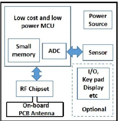
Basic hardware structure for a sensor node is shown in figure 2. Power source can be solar cell, mechanic harvester, a battery or a mixture of them. Most of the applications has computation load enough to use a small battery supplying energy to all the blocks on the node to handle sensing, signal processing, computation and communication tasks. Low power RF chipset with an antenna or an on-board PCB antenna is used to move data to RF layer and then to send data packages to other nodes in the network wirelessly. Node can be equipped with humidity, temperature, pressure, image, infrared, magnetic, etc. sensors on which physical phenomena is converted to analog signals to be read out by an ADC on MCU. MCU contains all the interfaces to communicate between ICs on the device, fast SPI interface for RF chipset, UART for peripheral ICs, ADC for sensor read-out, memory as a data storage and CPU core.
WSNs are used in many areas with promising applications; home automation to measure temperature, humidity, etc.; smart grid as a power gas and water meter; agriculture to monitor ripen time of crops; environmental monitoring to measure air quality, pollutants, forest fires and other disasters; mining to detect precense of gases; industry to monitor manufacturing processes and
conditions of industrial equipment; military for surveillance; and animal tracking [1].
Figure 2 Basic hardware structure of a node
Design optimizations both in hardware and software layers with special techniques for the purpose of battery life extension with the wireless link must be involved to achieve desired performances in an electronic device because key issue node life usually means battery life. Integration of wireless link to a sensor network requires management of data flow in the environment to prevent collisions, efficient use of air interface and safe arrival of data to a base station through a MAC (media access control) layer [2].
There are two kinds of applications of wireless network architectures, called infrastructure mode and ad hoc mode. In the infrastructure mode, each node links to a base station or intermediate node connecting data flow path to the base station and two way data flow between nodes supplied over the base station or intermediate node. On the other hand, in ad hoc mode source node sends the information to destination node directly if it is in the communication coverage or to another node to be forwarded until reaching destination node, called hopping [3].
Communication range for a sensor node is another cost related factor and depend upon carrier frequency, antenna size, working environment and transmit power. Longer communication range means less number of nodes in the network in return for cost and bandwidth contamination reduction.
Trends are integration of all the hardware blocks on a system with minimum cost, area and energy consumption with maximum range [3-6]. In these works, an ASIC is designed to achieve minimal energy consumption per bit and to implement sleep mode with asynchronous wake-up by hardware architecture and using new circuit technologies.
SAÜ Fen Bil Der 20. Cilt, 2. Sayı, s. 121-132, 2016 123 In this study, to reduce power consumption, software
techniques on the system level are employed and to drop the main objective cost containment, using both hardware and software techniques, a sensor node with a low cost ISM band FSK transceiver and an on-board antenna is designed. Complete system is tested in infrastructure mode architecture hardware because infrastructure mode based sensor network architecture is targeted due to its simplicity, higher base station transmit power, higher receive sensitivity and wide choice of frequency spectrum. Up to 131.25 year node life in theory with further potential extension, 4-5$ cost and 25m indoor communication distance are achieved.
2. CHOICE OF MODULATION AND FREQUENCY BAND
FSK is less susceptible to errors than ASK modulation because noise presents in amplitude and frequency modulation is resilient to signal strength variations in harsh environments.
FSK modulation has constant envelope modulation and does not require linear power amplifiers. Therefore, high efficiency nonlinear switching-mode power amplifiers can be used with simple demodulation hardware, so giving low cost in comparison to PSK hardware. Application frequency band must be chosen in regard to countries’ air interface regulations. For example, 915 MHz frequency band is not designated for unlicensed used in Europe by ETSI and CEPT. Instead, LPD433 and SRD860 license free bands with 10 mW ERP are allocated [7].
2.4 GHz (such as Bluetooth or Zigbee) networks have high data rates, but short communication distance. On the other hand, sub-gigahertz high frequency has small antenna size with more gain and longer distance with lesser power consumption in the expense of lower data
rate communication. Antenna in use effects
communication range and half wavelength dipole antenna sizes for different sub-gigahertz frequencies are shown in Table 1. Friis link equation based communication distance can be found from equation (1) and parameters are d distance, Pt transmit power, Pr receive power, Gt transmit antenna gain, Gr receive antenna gain, λ wavelength and L system loss factor.
Table 1. Half wavelength Dipole Antenna Sizes Hw. Dipole Antenna size 433 MHz 868 MHz 915 MHz 34.6 cm 17.3 cm 12.4 cm ( ) = ( ) (1)
3. LOW POWER DESIGN
Extension of battery life time of a sensor node communicated to other nodes over air requires various intensive software and hardware techniques to be implemented.
3.1. Dynamic Operation Modes
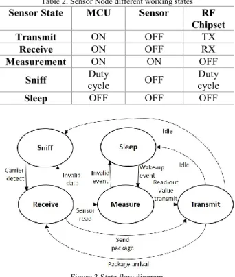
Hardware blocks on the sensor are shut down when unnecessary and powered up depending on anticipated or periodic activity or an event, leading to different operating modes, summarized in table 2 and figure 3. Sniff and sleep mode may look confusing at the beginning. In sniff mode, RF link activity is checked with periodic wake-up after shutting down all the hardware blocks. On the other hand, wake-up and sensor measurement in sleep mode happens when a triggering event occurs, such as key pad activity or threshold level crossing. Details of each state and state transitions are explained in the following sections.
Table 2. Sensor Node different working states
Sensor State MCU Sensor RF
Chipset Transmit ON OFF TX Receive ON OFF RX Measurement ON ON OFF Sniff Duty cycle OFF Duty cycle
Sleep OFF OFF OFF
Figure 3 State flow diagram
3.2. Voltage and Dynamic Frequency Scaling and Power Gating
As we know each integrated circuit is made up of cells and gates consisting of individual transistors. Each transistor is either placed in power-up or power-down network, whether it is analog or digital IC cell or gate such as LNA, mixer and differential amplifier in an RF IC and ALU, accumulator and Program Counter in a
124 SAÜ Fen Bil Der 20. Cilt, 2. Sayı, s. 121-132, 2016 digital IC. Each output node of cells and gates is pulled
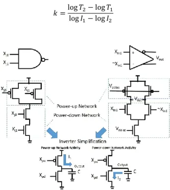
towards supply voltage charging output load capacitor or ground discharging output load capacitor depending on input activities of power-up and power-down network transistors. Concise concept sketch is shown in figure 4 for a NAND gate and differential amplifier.
As each IC is represented by multiple inverters, to get an idea about power and energy consumption, we need to look at well-known energy per cycle (2) (output load capacitor charged by I1 and discharged by I2) and power for f frequency with α activity (3) equations for an inverter. Only voltage and frequency having quadratic and linear dependency on energy can be adjusted on an IC. Therefore, supply voltage and frequency must be lowered as much as possible to reduce energy consumption, called voltage scaling and frequency scaling respectively. To decrease supply voltage causes increasing delay (6) so slowing down operating frequency [8]. In equation (6), k and α are technology related parameters and Vt is threshold voltage. As seen in equation (3), it is unnecessary to supply power to an IC with zero activity, and then it is shut down to save energy and static power consumption (represented by Ileak), this operation called power gating. In addition, single transistor current consumption in an IC, given in equation (4) for NMOS and (5) for PMOS, is decreased by voltage quadratically. W and L are transistor width and length and k is technology related parameter.
= + (2) = + + , 0 ≤ ≤ 1 (3) =1 2 − = ( − ) | (4) =1 2 − = ( − ) | (5) = ( ) 1 ≤ ≤ 2 (6)
3.2.1. Battery voltage scaling
Crucial metrics effecting lifetime for a small size battery are voltage and capacity (C-rate), one hour discharge rate (current) given with mAh. Peukert’s law states (7) as the discharge rate increases the battery capacity decreases or vice versa and battery voltage decreases gradually with capacity reduction [9]. In reality, variety of issues effects battery lifetime and complicating the estimation of capacity such as temperature, see figure 7.
= (7)
=log − log
log − log
Figure 4 Simplification of cells and gates in an IC
Variables are C capacity in mAh, I discharge current in mA, k the Peukert constant measured from two different discharge time and current and T time of discharge in h. You can see Peukert curves (a kind of curve fit method see figure 5) in figure 6 (A) created from sampled values of different batteries with different sizes for capacity vs. discharge current. In figure 6 (B), to reduce discharge current (or to increase capacity), our region of interest, up to a few 10s miliampere current, is magnified in x-axis. In this region with reduced discharge current, not only you get increased battery life but also there is less current consumption to save energy.
Figure 5 Measured and Peukert predicted capacities for Alkaline ZnMn02 AA size battery [9]
Advantage of our application is to have intermittent load that our periodic wake-up scheme brings (to be explained in the following section), allowing recovery time to
SAÜ Fen Bil Der 20. Cilt, 2. Sayı, s. 121-132, 2016 125 battery, so prolonging lifetime [10]. Primary Alkaline
battery is employed in the application due to higher energy density (or capacity), longer life, light weight, low cost and convenience to low current applications, see table 3 and figure 6.
Figure 6 Peukert Curves for different battery chemistries and sizes Advantage of our application is to have intermittent load that our periodic wake-up scheme brings (to be explained in the following section), allowing recovery time to battery, so prolonging lifetime [10]. Primary Alkaline battery is employed in the application due to higher energy density (or capacity), longer life, light weight, low cost and convenience to low current applications, see table 3 and figure 6.
Table 3. Cost per Wh and Wh per weight [11] Battery Type Cost $ per Wh Wh/kg Lead-acid 0.17 41 Alkaline long-life 0.19 110 Carbon-zinc 0.31 36 NiMH 0.99 95 NiCad 1.5 39 Lithium-İon 0.17 128
Because ICs on the sensor node can be run from supply voltage in the range of 2.2V-3.8V, there is large margin to exploit voltage scaling, first to reduce energy consumption and second to lessen battery discharge rate since energy and current consumption depends upon supply voltage quadratically. Therefore, voltage of the small size battery is chosen 3.0V by considering mid-point voltage, not around 2.2V not to fall below minimum voltage level due to continuous voltage decrease after reduced capacity, figure 7. This voltage must also supply minimum required frequency.
Briefly, by voltage scaling from 3.8V to 3V, there is 37.8% energy saving in theory with keeping peak RF data rate performance and range the same (TX power amplifier has its own LDO), acquiring quadratic reduction in current consumption and so increase in battery life at the same time. Actual situation is better because short circuit current brings additional linear saving in energy, which must be taken into account.
Figure 7 Battery voltage variation with different temperatures at 100mA discharge current
3.2.2. Dynamic frequency scaling
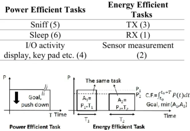
WSN’s become computationally intensive increasingly, so energy aware design is essential. Low power and low speed microcontrollers as an embedded system are used to achieve and manage this goal in the sensor node. In the design time, the embedded system knows power consumption, timing constraints and data behavior of all the hardware blocks of peripherals, communication and physical units, as seen in figure 2. In the precense of this information, tasks in an embedded system for the sensor node are treated in terms of energy efficiency. In the first case, power efficiency has the same outcome as energy efficiency, this kind of task is called power efficient task. System clock is scaled down as much as possible to minimize power and so energy consumption in linear
manner, considering successful execution or
performance constraint of tasks (end time). On the other hand, for energy efficient tasks, there is a cost function, namely power-delay product measured by Joule/bit or Joule/symbol and optimum value should be find by adjusting frequency, see figure 9. In our case, energy efficient tasks, TX, RX and sensor measurement, must be executed in the maximum speed of related hardware, RF chipset and sensor by adjusting system clock, because there is nearly constant power consumption whether slow speeds are acquired or not. Hence, high speed adjustment brings energy efficiency, efficient use air interface, low latency and fast throughput.
126 SAÜ Fen Bil Der 20. Cilt, 2. Sayı, s. 121-132, 2016 Table 4. Power and energy efficient tasks with static priorities
Power Efficient Tasks Energy Efficient
Tasks
Sniff (5) TX (3)
Sleep (6) RX (1)
I/O activity display, key pad etc. (4)
Sensor measurement (2)
Figure 8 Goal of power and energy efficient tasks 3.3. Low Power Wake-up Scheme
To achieve extended battery life, nodes and base should remain in sleep mode until data sent or received. Because exact data burst arrival time is unknown due to sleep mode, nodes or base awaken periodically to receive and execute command or user function within a burst, then inform back or send acknowledge for safe hand-shaking protocol to the node communicated. As it is understood from the scheme, source node must keep sending the bursts until back information or acknowledge arrived from a neighboring node or for the wake-up period of a neighboring node in worst-case, see figure 10. Aforementioned wake-up scheme is shown in figure 9 and power consumption is reduced by %(1-D) of receive power. Twb and Twn are wake-up periods with Db and Dn duty cycles for base and nodes wake-up scheme respectively, which are done by both hardware and software co-design. Wake-up time point for nodes does not intersect generally due to process variations on hardware causing drift, different programmed value and different power-on time so different timer start time. Latency results from the wake-up scheme during data flow to base station is negligible in sensor networks.
Figure 9 Low power wake-up scheme
In addition to periodic wake-up, an external event can trigger awakening to exchange data between two neighboring nodes, depending on the application nature such as external event or threshold level crossing. The chipset used in this kind of applications allows multiple modulation, frequency bands and channels to be selected and used one at a time. Additional OOK
modulation is usually added to the transceiver for wake-up triggering because it requires 50% less power than FSK modulation during transmit [1], [12]. In general, most of the power consumption comes from sleeping and RX listening in the wake-up scheme and reduction of this power directly effects node life, (lowest one 270nW) [1]. As nodes enter the sleep mode shutting down all receive chain blocks, the PLL in the frequency synthesizer put constraint on awakening time TwD as in frequency hopped links and this time must be equal to the total of PLL stabilization and lock time and crystal oscillator start-up time at least for a communication channel to exist. In addition, power efficient designed non-linear TX power amplifier is the most power consuming part in TX chain, so estimation of Tw of neighboring node from received package to reduce TX power amplifier activation is desired [3]. This feature is added in S-MAC designed sensor networks by synchronization bytes [2]. Wake-up period and duty cycle can also be adjusted according to data traffic in the network.
4. DATA FRAME STRUCTURE AND MAC LAYER Wireless link traffic needs to be regulated to prevent collisions and data loss; and hence generic package structure in figure 11 below is used. First two
components of data frame is preamble and
synchronization bytes, implemented on hardware layer. A preamble consist of a sequence of one and zeros to sense carrier and synchronization bytes indicates from which bit position of the frame the actual data to be started to get correctly whole package to prevent data misalignment on bit level. Device and destination ID for node and base singulation; package ID and package count in case of data, frame and package loss as a retransmit reference; and package size to adjust data length during high and low data traffic and to enhance low power are attached to the frame and all of them are fixed in their position and length. Data bytes section contains user specified functions and commands in fixed positions to set up network features, to handle data flow and to adjust power consumption such as ID, duty cycle, wake-up period and frequency. CRC (cyclic redundancy check) and parity check are added to detect errors in data at the end of the frame. This frame is sent as a burst through FIFO (first in first out) register in the transceiver. Collision arbitration is also done in hardware by capture effect, called co-channel interference rejection. After carrier from a sensor node is detected, hardware is locked to that carrier and data frame is acquired from the connected sensor node although other signals are present in the environment and a stronger signal is required to restart communication and to get a new frame.
SAÜ Fen Bil Der 20. Cilt, 2. Sayı, s. 121-132, 2016 127 Figure 10 Low power wake-up scheme between two nodes
Figure 11 Wireless link frame structure
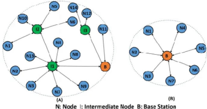
Figure 12 Wireless sensor network architecture abstraction 5. WIRELESS SYSTEM ARCHITECTURE In figure 13-B, nodes send information to base station even if actual destination is another one and the boundary of network is limited with base station receive sensitivity (LNA) and transmit power (Power Amplifier).
In figure13-A, each intermediate node (relay) added to the network to extent the coverage needs to know which intermediate node or base to send package for message relay. These relay nodes can be used to increase energy efficient data gathering and maximize network life time by alleviating data traffic on the base node. Latency coming from intermediate nodes does not critical for this kind of applications.
= + (8)
Figure 13 Infrastructure mode architecture (A) intermediate nodes used to extend coverage (B) base station only
Placement of sensor nodes for energy efficiency in the field is crucial since energy consumption is strong function of distance [2], [4]. Energy required by sending one bit is given in (8) a dissipated energy in electronics, b transmitter efficiency and α path-loss exponent (α ≈ 4-6 for in-door environments) [4]. Therefore, in the cost of more sensor nodes, energy can be saved further by placing them efficiently in the network [13].
6. SOFTWARE
Publicly available operating systems such as TinyOS [14] and DISSense [15] can be easily integrated into an application with ad hoc routing. For ad hoc mod wireless sensor networks, many protocols publicly available such as ZigBee.
For a typical application, basic code overview is shown in figure 15 for base and nodes. The following functions are supported (1) exploitation of wake-up scheme both for base and nodes (2) user functions and commands (3) network parametrization e.g. Frequency, ID, threshold values, Tw and D (4) node addition to the network.
128 SAÜ Fen Bil Der 20. Cilt, 2. Sayı, s. 121-132, 2016 Figure 14 Typical code overview for base and node
7. ANTENNA DESIGN AND TX AND RX DRIVER CIRCUIT
PCB designed tapped loop antennas with monostatic diversity are commonly used in WSN for short range due to cost and simplicity. They have the same far-field radiation pattern as the small dipole antenna placed to normal to the loop plane and directivity (D0) is also the same 1.5. In equation (9), radiation resistance is given for free space conditions, A loop surface area, N number of turns and λ wavelength [16]. Antenna inductance is stated in equation (10) with loop and wire inductances with h metallization thickness and w width of trace [16]. Gain is given in (11) with D directivity and E efficiency, low for loop antennas. At high frequencies, longer distance communication can be achieved with small size loops in comparison to low frequencies [17] and that is why 868 MHz band is chosen. 868/915 MHz Dual Band Symmetric Cross Tapped Loop Antenna designed on PCB is proposed for sensor node and base station, look at [17] for dimensions, to reduce high impedance with tapping technique with better radiation efficiency. Differential TX driver amplifier efficiency is high due to the high real part of antenna impedance (explained in [16] in detail ) rather than antenna efficiency and |S11| (matching for maximum power transfer) [17].
= 31171 (9) = + = 2m √ ln √ − 0.774 + = 2m √ ln √ − 0.774 +m √ (10) =(0.35ℎ + 0.24 ) 1000 (Ѳ, ф) = (Ѳ, ф) (11)
However, loop antennas have some drawbacks. Loop size must be large enough to achieve high radiation resistance to achieve matching. Loop antennas are also vulnerable to detuning coming from technological dispreading in semiconductors, variations in design dimensions on PCB, component value tolerances, any metallic objects in the vicinity of the antenna and hand
effect due to high Q antenna. Therefore, Back Inverted-F Antennas are used for matching purposes requiring no or a few external components, less sensitive to the detuning due to lower Q and higher gain. In addition, overall RF link efficiency of BIFA is 10dB more than tapped loop in general [16].
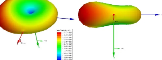
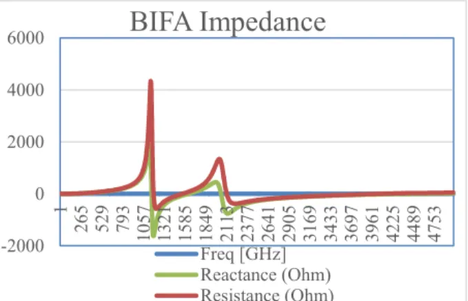
BIFA is designed on FR4 lossy substrate whose properties is given in the table 5 below. High dielectric substrate gives lower Q antenna so more bandwidth and less field leakage among traces of antenna and ICs on the PCB in the expense of higher loss. BIFA design dimensions, gain and input impedance and resonance frequencies are shown in figure 15, 16 and 17 below respectively. There is no ground plane in the design since ground reduces gain. By using half circuit concept for 8.7-j66 differential port impedance, matching, bandwidth and antenna pin current and voltage at 10 dBm RF source for maximum ratings are exhibited in figure 18. -24.02 dB S11 is obtained at 879 MHz with 5 MHz bandwidth and 35 Q with only three external components 1.1pF capacitor and 2x36nH inductors (12) and (13).
Table 5. Properties of PCB used in the design Double Layer Copper
FR4 Substrate Properties and Sizes
Value
Dielectric Thickness 0.5 mm
Dielectric Constant (Ɛr) 4.6 - 4.7
Copper Thickness (h) 35 um
Loss Tangent (tan(δ)) 0.018
Size 4 cmx4 cm
Figure 15 BIFA structure and design dimensions
SAÜ Fen Bil Der 20. Cilt, 2. Sayı, s. 121-132, 2016 129 Figure 17 BIFA resistance and reactance vs frequency and resonance
frequencies
Figure 18 BIFA S11, impedance matching with capacitor and voltage
and current for 10 dBm RF source power
= Γ = (12)
P = P (1 − |S | ) (13)
Two discrete inductors 36nH and a 1.1 pF capacitor are used to match chip output impedance 8.7-j66 and two inductors are land on the RF pads on the antenna design. In this configuration, antenna 35 Q (325/9.28) corresponding nodal quality factor in matching circuit limits the bandwidth of the system around 5 MHz. 5 MHz bandwidth is defined based on -10 dB points in S11 corresponding to %10 power loss in matching circuit and for our design 5 MHz bandwidth is more than enough. Maximum ratings in RF pin voltage and current must be considered in impedance matching network, 4Vpp RF pin voltage for the RFIC.
Any variations in chip output impedance semiconductor process, component values and design dimensions are compensated by the automatic tuning circuit at the output of the TX differential power amplifier. Automatic tuning circuit puts into use the 4-bit capacitor bank (2.2pF - 3.2pF) depending on matching with B7 default (2.7pF) value by looking at current phase to fix any deviation from 0 degree [16].
The range is estimated from link budget by using simple path loss model (12) and n is propagation exponent (n=2 free space, obstructed buildings n=4-6 and n=2-3 obstructed factories). Received power threshold for 10-5 BER and maximum transmit power are 0.794 pW (-91dBm) and 5 mW (7dBm) obtained from IC datasheet. Communication distance is estimated around 32.86 m for 0.45 (-3.5 dBi) antenna gain and 6 propagation exponent considering indoor environment and it is found 975 m for outdoor environment from Friis Link Budget.
= 10 log ( ) = =
( ) = (14)
8. SENSOR NODE DESIGN
Long term battery driven wireless link perspective considered, by using a low cost FSK ISM band programmable RF transceiver a sensor node is designed, design and scheme shown in figure 19 and figure 20, and DC and AC characteristics are summarized in table 6. Circuit components and metal traces are away from the antenna to prevent gain penalization. Parallel decoupling capacitor bar is used to achieve AC short at Vdd, to remove noise as filters and to avoid ripple for regulation. Any type of sensor can be integrated into the sensor node because MCU has all the interface required such as ADC, UART and SPI. Internal temperature Sensor on MCU is utilized and values are obtained by ADC interface. SPI interfaces with high speed internal oscillator are used to communicate with RF chipset. Wake-up scheme is implemented on-chip MCU slow oscillator which has 100nA-500nA current consumption.
Data is first acquired from sensor by a slow interface and buffered in RAM and then put maximum speed RF layer through fast SPI interface into FIFO register to send each byte consecutively with byte-level hand-shaking, utilizing burst sending advantages, energy saving and lessening frequency band allocation time.
As the nature of the wireless network requires, nodes and base stay in a changing environment effected by temperature, moisture and movement. Temperature variation causes internal oscillator frequencies to drift from original values, changing clock resulting in cumulative errors in data frame and sensor read-out values. After calibration in MCU, frequency deviation with respect to room temperature is %5 at most, which can be tolerated by low-speed sensor and SPI interface and hand-shaking procedure can come to environmental challenges’ rescue. -2000 0 2000 4000 6000 1 265 529 793 1057 1321 1585 1849 2113 2377 2641 2905 3169 3433 3697 3961 4225 4489 4753
BIFA Impedance
Freq [GHz] Reactance (Ohm) Resistance (Ohm)130 SAÜ Fen Bil Der 20. Cilt, 2. Sayı, s. 121-132, 2016 Figure 19 Sensor node with ISM band FSK RF Transceiver
Figure 20 Sensor node scheme with ISM band FSK RF Transceiver Table 6. Sensor Node Measured DC and AC Characteristics Vdd=2.7V and T=27
°C
Sensor Node DC and AC Characteristics Frequency Bands ISM band 433, 868 and 915 MHz
with 400kHz BW Full duplex Communication
Range 100m Outdoor, 30m indoor Data Rate 0.6 kbps-115.2 kbps Supply Voltage 2.2V – 3.8V
Stop mode current 300 nA(RFIC) + 100 nA(MCU) = 400 nA with pin activation wake-up Sniff mode current 300 nA(RFIC) + 500 nA(MCU) =
800 nA (MCU slow osc. running) PLL Start-up time 200 us, lock time 30 us
with 8mA current consumption Crystal Oscillator Start-up time 2 ms with 300nA
current consumption
MCU + sensor 2.3 mA @ 8MHz working cond. (MCU)+0.2 mA (On-chip sensor) TXmax Current 23 mA (RFIC TX mode) + 2 mA
(MCU) = 25 mA @868MHz TX Power
(simulation)
-3.5 dBi antenna gain + 7 dBm output p. = 3.5 dBm (2.2 mW) with PA 50 us turn-on RX Current 10.7 mA (RFIC RX mode)+ 3.9 mA @12MHz (MCU)= 14.6 mA @868MHz RX sensitivity (datasheet) -110 dBm BER 10-3 BW=67kHz BR=1.2 kbps
Ambient Opt. Temp. (datasheet)
-40 - 85 °C temperature compensated
Antenna Type Back Inverted F antenna
Cost 4-5$
9. RESULTS AND DISCUSSION
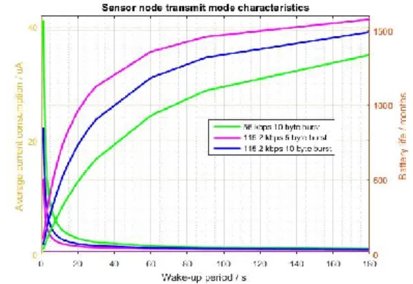
To test transmit mode performance, sensor nodes equipped with temperature sensors running with (two 1.5V battery pack) 3.0V 1000mAh alkaline ZnMnO2 AAA size battery shown in figure 6 with pink color are realized with similar software and hardware to section 6 and section 2-8. 25m 868 MHz RF link between base station and sensor node is established successfully. In this set-up, temperature information is send to the base periodically with a package length requiring 2 mA, 23 mA and 0.2 mA during TX for MCU, RFIC, Sensor respectively and current consumption is 800 nA during sniff mode. With the wake-up scheme, battery life time is seen in the graph for different package lengths, wake-up periods and different data rates [18] by using an energy model (15) and (16) similar to proposed in [19].
= + + (15) = + . + . = + + . = . = # = + + (16) = + . + . = + + .
SAÜ Fen Bil Der 20. Cilt, 2. Sayı, s. 121-132, 2016 131 Figure 21 Current consumption during sleep
Figure 22 Transmit mode current consumption in uA and battery life in h
Figure 23 Receive mode current consumption in uA and battery life in h
With this results, we conclude that;
Battery life time is heavily depends upon duty cycle and wake-up period current consumption. Sniff current 0.8 uA is the lower bound for the current consumption, which must be fallen down during sleep mode. Battery life time with 115.2 kbps 10 byte package and 180 second wake-up period with 0.8 uA sniff current consumption is 1490 months (124.17 years) corresponding to 0.92 uA average current consumption in theory. This value is 1575 months (131.25 years) for 115.2 kbps 5 byte package and 180 second wake-up with 0.8 uA sniff current in theory.
Wake-up period must be increased because most of the time sensor nodes inactive. In this case, other energy harvesting methods can be considered such as mechanic vibration or solar energy.
TX bytes can be reduced such as sending bytes when necessary, just by sending difference from last value, or coding.
Less current consuming TX and RX transceiver with high data rates can be used.
Average current decrease results in less number of waste batteries environmentally.
Advantages of our design in comparison to the similar works, see table 7,
Complete design and explanation of hardware from MCU level to RF level
Power saving modes by using software techniques brings over 100 year battery life time
No ASIC design cost and time reduction with the utilization of a designed RFIC
25m indoor and 100m outdoor long working distance with low power consumption feature
4cmx4cm small size with low BOM (bill of materials) list, so low cost around 4-5$
Can be easily integrated to any system to move data to wireless link
Low sniff mode current 800nA @3V supply voltage. Opportunity to employ other power harvesting
techniques such as solar cells and vibration
Low sniff mode current 800nA @3V supply voltage brings extended battery life for long period duty cycled applications.
As a future work, for an additional feature, modulation diversity can be exploited, self-monitoring [14] capabilities can be added and if low battery levels are detected, modulation can be switched to OOK modulation because it requires 50% less power than FSK. MFSK has also better energy efficiency than MPSK at higher M-ary modulation formats for a given BER. To reduce sniff mode current, MCUs produced in new technologies can be employed. In addition to that, link budget can be improved with single ended meandered PCB wire antenna with differential to single ended balun because it has higher gain than BIFA in a given area. Table 7. Comparison of different sensor nodes (parameters are obtained from datasheets) Feature Supply voltage [3] WISE NET [20] DOZE R [14] TINY OS [21] MIC A2 Our Work 1V 2.5V 3V 3V 3V TX Current 24 mA 16.1m A 17 mA 29.5 m A 25 mA
132 SAÜ Fen Bil Der 20. Cilt, 2. Sayı, s. 121-132, 2016 (MCU+T X) RX Current (MCU+R X) 2 mA 12.63 mA 9.5mA 15 m A 14.6 mA Sniff mode current 3.5 uA 6uA 10uA 110 uA 0.8 uA Speed 100 kbp s 75 kbp s 19.2kb ps 250 kb ps 115.2k bps Indoor Distance 10m - - - 25m REFERENCES
[1] M. Magno, S. Marinkovic, B. Srbinovski, and E.
M. Popovici, “Wake-up radio receiver based power minimization techniques for wireless sensor networks: A review,” Microelectronics J., vol. 45, no. 12, pp. 1627–1633, 2014.
[2] N. Kumari, N. Patel, S. Anand, and P. P.
Bhattacharya, “Designing Low Power Wireless Sensor Networks : A Brief Survey,” pp. 4447– 4456, 2013.
[3] C. C. Enz, A. El-Hoiydi, J. D. Decotignie, and V.
Peiris, “WiseNET: An ultralow-power wireless sensor network solution,” Computer (Long. Beach. Calif)., vol. 37, no. 8, pp. 62–70, 2004.
[4] J. M. Rabaey, J. Ammer, T. Karalar, B. Otis, M.
Sheets, and T. Tuan, “PicoRadios for wireless sensor networks: the next challenge in ultra-low power design,” 2002 IEEE Int. Solid-State
Circuits Conf. Dig. Tech. Pap. (Cat.
No.02CH37315), vol. 1, pp. 200–201, 2002.
[5] S. Oshima, K. Matsunaga, and T. Kondo,
“Ultralow-power Sensor Node with Nanowatt Wireless Circuit Technology.”
[6] EnOcean, “Scavenger Transceiver Module STM
300 STM 300C,” EnOcean Appl. Notes, no. November, 2012.
[7] P. Note, “ERC Recommendation 70-03,” no.
February, 2014.
[8] C. Hu, Low Power Design Methodologies.
Kluwer Academic Publishers.
[9] J. Larminie and J. Lowry, Electric Vehicle
Technology Explained. Wiley, 2012.
[10] M. Jongerden and B. Haverkort, “Battery
modeling,” p. 18, 2008.
[11] All About Batteries, “Battery energy - What
battery provides more?,” AllAbout Batter., pp. 1–3, 2015.
[12] P. D. Bradley, “An ultra low power, high
performance Medical Implant Communication System (MICS) transceiver for implantable
devices,” 2006 IEEE Biomed. Circuits Syst. Conf., pp. 158–161, 2006.
[13] F. Almajadub and K. Elleithy, “Performance
Advancement of Wireless Sensor Networks using Low Power Techniques and Efficient Placement of Nodes.”
[14] J. Hill, R. Szewczyk, A. Woo, S. Hollar, D.
Culler, and K. Pister, “System architecture directions for networked sensors,” ACM SIGOPS Oper. Syst. Rev., vol. 34, no. 5, pp. 93– 104, 2000.
[15] U. M. Colesanti, S. Santini, and A. Vitaletti,
“DISSense: An Adaptive Ultralow-power
Communication Protocol for Wireless Sensor Networks,” Proc. 7th IEEE Int. Conf. Distrib. Comput. Sens. Syst., pp. 1–10, 2011.
[16] C. Chavez, “Antenna Development Guide for the
Si4020 , Si4320 & Si4420 ISM Band FSK EZRadio ® Chipsets,” pp. 1–56, 2009.
[17] “Antenna Selection Guide For the RF12 ISM
Band FSK Transceiver,” pp. 1–37.
[18] S. Labs, “Battery Life Estimator &
Calc_BatteryLifeCalculator_v1.” .
[19] G. Terrasson, R. Briand, S. Basrour, V. Dupé,
and O. Arrijuria, “Energy Model for the Design of Ultra-Low Power Nodes for Wireless Sensor Networks,” Procedia Chem., vol. 1, no. 1, pp. 1195–1198, 2009.
[20] N. Burri, P. Rickenbach, and R. Wattenhofer,
“Dozer: ultra-low power data gathering in sensor networks,” IPSN ’07 Proc. 6th Int. Conf. Inf. Process. Sens. networks, 2007.
[21] M. Hempstead and N. Tripathi, “An ultra low
power system architecture for sensor network applications,” Archit, 2005.
![Table 3. Cost per Wh and Wh per weight [11] Battery Type Cost $ per Wh Wh/kg Lead-acid 0.17 41 Alkaline long-life 0.19 110 Carbon-zinc 0.31 36 NiMH 0.99 95 NiCad 1.5 39 Lithium-İon 0.17 128](https://thumb-eu.123doks.com/thumbv2/9libnet/4375385.73756/5.918.486.797.267.511/table-cost-weight-battery-alkaline-carbon-nicad-lithium.webp)
