Semiconductor Science and Technology
Electronic structure of Ge-Si superlattices grown
on Ge (001)
To cite this article: O Gulseren and S Ciraci 1991 Semicond. Sci. Technol. 6 638
View the article online for updates and enhancements.
Related content
Structure, properties and applications of GexSi1-x strained layers and superlattices S C Jain and W Hayes
-Electronic structure of (111)Si/Ge superlattices
J M Bass and C C Matthai
-Ultrathin SimGen strained layer superlattices-a step towards Si optoelectronics
H Presting, H Kibbel, M Jaros et al.
-Recent citations
Some aspects of the physics of man-made semiconductor heterosystems: superlattice electronic structure and related topics Pierre Masri
Semicond. Sci. Technol. 6 (1991) W 1 . Printed in me UK
I
I
Electronic structure
of Ge-Si
superlattices grown on Ge
(001)
0
GIilseren and S
Ciraci
Department of Physics, Bilkent University, Bilkent 06533, Ankara, Turkey Received21 January 1991, accepted for publication 13 February 1991
Abstract. We have studied the electronic energy strudure of pseudomorphic GedSi, superlattices by using the empirical tight-binding method. Effects of the band offset. sublanice periodicity and the lateral lattice constant on the transition energies have been investigated. We found that GedSi, superlattices grown on Ge (001) can have a direct band gap, if m + n = 10 and m = 6. However, optical matrix elements for in-plane and perpendicular polarized light are negligible for the transition from the highest valence band to the lowest conduction band state
at
the centre of the superlatlice Brillouin zone.The novel properties discovered in the electron systems of lower dimensionality have created a major impact in solid state electronics leading to new concepts in electronic de- vices. In this context, it is hoped that pseudomorphic Si-Ge superlattices can compensate for the shortcomings
of
silicon and CM open new horizons in the applications of Si-baseddevices in photonics. In
an
effort to fabricate a high car- rier mobility direct-band semiconductor, the Si-Ge superlat- tices grown on the (001) substrate have been the focus of at- tention 11.21. While the electroreflectance measurements of SidGe, grown on Si (001) have indicated new optical transi- tion [l], theoretical studies [3-61 showed that the difference between the direct and indirect band gap, 6E =-
E&,,,,decreases with increasing n, but the gap is still indirect. For example, it was found [3,4] that 6 E is
as
smallas
0.07 eV for the largest superlattice periodicity (2n = 12) one can obtain for SiJGe, grown on Si (001). Moreover, optical matrix el- ements of the transitionto
the lowest zone folded states were found U) be small [7].In view of evidence indicating that the strained Si,/Ge, laterally restricted
to
Si (001) hasan
indirect band gap, attention has been drawn to the Si-Ge superlattices with different structural parameters [8,9]. In fact,as
ar-
gued earliera
pseudomorphic superlattice represented by {Sii-xGex)n,all /{Si,-yGey]m,o,, provides several degrees of freedom for controlling the electronic properties. For exam- ple, in the superlattice with x = 0 and y=
1 the lateral lattice constant a and the superlattice periodicity, n+
m ,(also n and m itsel0
are
important parameters for controlling the electronic structure. Since the lateral lattice constant of asubstrateSi,-,GeZ(001) can vary between U? (equilibriumlatticeconstant of Si, i.e. 5.43
&J")
andor,
the snblattices grown in registry with this substrate undergo a lateral com- pressive (expansive) strain, while the lattice constant in theperpendicular direction expands (contracts). This gives rise to a uniform tetragonal distortion if the misfit dislocations are prevented from forming.
In this paper we first investigate the effect of the struc- tural paramekrs on the direct and indirect bmd g a p of the pseudomorphic Si-Ge superlattices. Guided by these find- ings and based on the electronic structure calculations, which were performed for several supercells by using the empirical tight-binding method, we determine the structural parame-
ters which make the band gap direct.
It is known that Si-Ge superlattices generally make type- I1 band alingments, such that the edge of the conduction band and the top of the valance band
occur
in the Si and Ge sublat- tices, respectively. To examine the lowest conduction band statesof
the Si,,/Ge,, we concentrate on the Si-sublattice. The minima of the conduction band of bulk Si occur along the six equivalent[Ool]
directions. These directionsare
labelled asA in the (fcc) Brillouin zone (BZ)
of
the bulk Si. In the su-perlatticegrown on the (001) plane, four A directions, which are labelled by A , , coincide with the r M direction of the su-
perlattice BZ
(see
inset of figure 1). The remaining twoare
along thesuperlattice direction [001] and are labelled by A,. Bands along A, are folded. In the absence of strain in the Si- sublattice the minimumof
the lowest conduction band stale along the r M direction of the SBZ occurs at relatively lower energy than the lowest folded states along theTZ
direction. Moreover, the lowest conduction band state was found to be itinerant [3,6]. This is the situation for the strained Si,/Ge,(n
5
6) superlattices grown on the Si (001). If, however,a
tetragonal strain is induced by forcing the Si sublattice to have all>
a? the bands along A,, and A,are
expected to experience different shifts.We explored this situation by examining the bands of Si and Ge supercells under tetragonal strain. The variation of
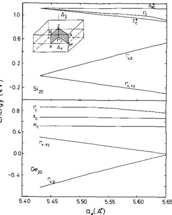
Electronic structure of Ge-Si superlanices earlier in several calculations. For Si, in figure 1 the IOW-
est conduction band state Z* along the TZ direction and the minimum A; of the lowest conduction band along All are both lowered
as
all + o r . Moreover, the stateZ*
is low-ered below the A i state, and the energy difference
E A .
-E=*increases with increasing all
-
asiwe
note that the Z* state band along A,, which is folded toTZ
upon the superlath formation. Similary, the splitting of the valance bands in- creases as all-
a y , so that the p,-like state raises towards Z*, butp, statesare
lowered.II
corresponds to the minimum AL
!'
of the lowest conduction-0 O0: 4
....
%o:---::---i
10 - 0.6 - 0 2 ~ -0.2 - W Re 0 4 - 5 L O 5 4 5 5 % 5 55 5 60 5 65 a,( A')Figure 1. Variation of the energy of the lowest conduction band states
(c,
Aic alongTZ
and r M directions) andrc
state and highest valance band states(rv,z
andrv,xy)
ofSi, and Gem supercells as a fundion of the lateral lattice constant all. The symmetry points and directions of the superlattice Brillouin zone are shown in the inset.
the lowest conduction and highest valance bands of Si, and Gem superlattices are calculated
as
a function of all. Our re- sultsare
presented in figure 1 for m = 20. In these calcu- lations the perpendicular lattice parameter a, corresponding to a given all are calculated by using elastic constants. Ear- lier it was shown that aL obtained from the Poisson ratio is in compliance with that obtained by using ab initiocal-
culations [lo]. The results of the fully optimized structure calculations on the Si-Ge superlattices show that in general
aL
differs slightly from the valueobtained by using thePois- son ratio. Moreover, interlayer spacings in the sublatticesare
not homogeneous [3,41. Nevertheles, in viewof
Iheaccu- racy obtainable from the empirical tight-binding calculations the structural parameters obtained from the elastic constants suite to the objectives of our calculation. The energy param- etersgivenbyLiandChung[Illarescaled [I21 byd-? with the scaling exponent q=
2 when the interatomic distancesof the sublattices deviate from their equilibrium values in the presence
of
the strain. Since splitting of the top of the valence band state at the point, &E,,,,,
is related to the de- formation potential b, and strain components ea and czz asSE,, = %(ezz
-
ea), the exponent q can be fitted lo the deformation potential. Expressing the deformation poten- tial [13] in Lerms of the strain components, first and second nearest-neighbour tight-binding energy parameters and q , we find q-
1.8. This justifies the value of exponent 7 = 2 usedI i
0 2 4 6 8 10
m
Figure 2. Variation of the relevant transition energies
of GedSi, with the number of the Ge layers m. The superlattice is laterally restricted to the Ge (001) surface
so that all =
a r
and m + n = 20. (A€, = 0:31 eV).In view of the above discussion one concludes that the lowest conduction band state, A;,
can
be folded to the cen- tre of superlattice BZ to yield a direct band gap for a pseudo- morphic GeJSi, superlattice grown on Ge (001). Thiscan
be achieved for certain superlattice periodicity. For exam- ple, if
the
lowest conduction band state A; were occured exactly at k,=
0,
k, = 0, and k, = 8 ~ / 5 a for a strain-free Si, superlattice, this state A; would fold tor
for 1 = 20 (which h a sG,
=
2x/5a for the magnitudeof
lhe shortest re- ciprocal vector). For a strained GeJSi, superlattice grown on Ge (001) A; does not appear exactly atk,
= 8a/5a.However, small deviations from the value 8a/5a can ac- counted by varying lattice strain and sublattice periodicity
but by keeping 2(m
+
n ) = 20 so that the minimum valueA*, may occur at I' point upon folding. Figure 2 shows the
variation of various transition energies
as
a function of m for the strained Ge,/Si, superlattice grown on Ge (001). For 55
m5
6 the lowest conduction band state occurs atr,
at- tributing directness to the band. The superlattice with m = 7 lies at the borderline and beyond m = 7 the Ge character dominates and thus the lowest conduction band state at R dips below that atr.
Form<
5 the lowest conduction band state starts to occur either at 2 or alongrZ. These
results are in agreement with the band structure of Gem/Si, which are calculated by using the self-consistent pseudopotential cal- culation (91as
wellas
experiment [21. Note that the calcu- lated transition energiesas
a functionof thenumber of the&0 Gulseren and S Ciraci
layers in the Ge,,,/Si, superlattice is not continuous, but dis- play wiggles in figure 2. This is due to the discrete variation
of
m, which leads to discrete changes in the geometrical pa- rameters and hence to the discontinuous variation in (folded) band energies.We note that the transition energies in figure 2 are ob- tained from the band structure calculations of the Ge,,,/Si, superlattice. Because of the emprical nature of the method the elements
of
the Hamiltonian matrix (i.e. self-energies and hopping energies)are
inputs in OUT calculations. In this context, the valueof
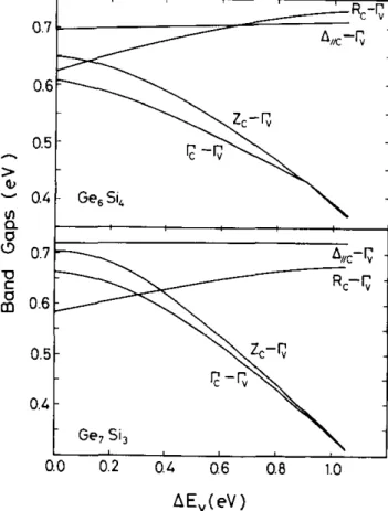
the band offset is implemented in our calculations by upshifting the self-energies (or the diagonal elements of the Hamiltonian matrix) of the Ge orbitals byAE,. The value of the band offset we used in our calcula- tions wasobtainedfrom theearlierab initiocalculations [IO]. Since the band offset is the crucial parameter which influ- ences the conduction band structure of the superlattice, we investigated whether the value of AE, affects our conclu- sions regarding the directness of the band gap. In figure 3 we present the variation of the transition energies
as
a
func- tion of AE, calculated for GedSi, and Ge,/Si, both hav- ing all = a;” The band gapof
Ge6/Si, is directas
longas AE,
5
1
dV, but the difference between the direct and indirect gap decreasesas
AE, increases. In contrast, the di- rectness of the band gap of Ge,/Si, is sensitive to the value of the band offset. For example, the R,r, transition energy becomes smaller than the lowest direct transition energy and thus the gap becomes indirect if AE,5
0.3 eV. Note that the band offset AE, is affected due to the upshifting of theA E v ( e V )
Figure 3. Variation of the transition energies with respect to the band offset, A€, for (top) Ge6/Si, and (bonom)
Ge7/Si3. Superlattices are restricted to the Ge (001).
maximum valance band state by the one-third of the spin- orbit coupling energy A,. The value
of
A, is negligible for Si (A,,=
0.04 eV) but significant for Ge (A, = 0.3 eV). Consequently, owing to the spin-orbit coupling AE, is in- creased by 0.1 eV for a GdSi superlattice [lo]. The tran- sition energies illustrated in figure 2 are calculated by AE,which does not include the spin-orbit coupling. As
a
matterof
fact, this effect is neglected in several studies of Si/Ge su-perlattices. However, this effect is implicit in the discussion
of
figure3
in which AE, is takenas
a parameter.Table 1. Calculated optical transition energies (eV) from p l h highest valenm band state to the qth lowest
conduaion band state (i.e. Evp
-
ECp) ?I the zone centre. All optical matrix elements for the in-plane(11)
and perpendicular (I) light polarization are negligible, except those indicated by stars have small but finile values(- in au). ( A & = 0.31 eV).
Ge&/Ge (001) Ge&/Ge (001)
Energy
11
Pol.I
Pol. Energy11
Pol.I
Pol.0.62 €.I -€,I 0.57 €,I - E a 0.87 0.84 * €,I - Ev3 0.89 0.85 * 0 66 0.88 0.89
From rhe above discussion it becomes clear that Ge6/Si, grown
on
Ge (001) is a direct band gap semiconductor. How- ever, the directness of the band gap can have i m p o m t tech- nological implications only if the lowest direct transitionsare
allowed and the value of the related uansition matrix ele- ments are subtantial. To this end we calculate optical matrix elements for in-plane and perpendicular polarizations for di-rect
transitions atr.
In the emprical tight-binding method the optical matrix element can be approximated [I41 byT*-,,,,
I
ci;,(k)c:”(w
D I ’ d . 2 ”
where C:,(k) is the
coefficient
of the Blwh sum,n,
is the Bravais lartice vector and T””, is the distance between thenuclei, v and U’, oi labels the atomic orbitals. The energy in-
tegral,EkI: = (#DI(~)lH~#DI,(r
-
R,-
T ” ” , ) ) , corresponds to the energy parameter in our calculation, andt
is the p- larization vectorof
the light. The optical matrix elements calculated from the above expresion and summarized in lil-ble 1 are crude but indicate that the direct optical transitions of Ge,/Si, and Ge,/Si,
are
not significantas
faras
photonics is concerned. For the light polarized along the superlattice axis (perpendicular polarization), all optical matrix elements ofGe6/Si, andGe,/Si, arenegligibleexcept for the transition from the highest valance band to the second lowest conduc- tion band state (Ev, i Ec2) at the centre of BZ. In the case OfElectronic structure of Ge-Si superlatlices [2] Pearsdl T P, Vandenberg J M, Hull R and Bonar J M [3] Froyen S, Wood D M and Zunger A 1987 Phys. Rev.
[4] Ciraci S and Batra I P 1988 Phys. Rev. B 38 1835
Ciraci S, Baratoff A and Batra I P 1990 Phys. Rev. B [5] People R and Jackson S A 1987 Phys. Rev. B 36 [6] Ciraci S, Giilseren 0 and Ellianioglu S 1988 Solid [7] Hyberstsen M S and Schlijter M 1987 Phys. Rev. B
Wong K B, Jams M, Morrison I and Hagon J P 1988 [8] Gel1 M A 1988 Phys. Rev. B 38 7538
191 SatDathv S. Martin R M and Van de Walk C G 1988 1989 Phys. Rev. Left 63 2104
B 36 4547; 1988 Phys. Rev. B 37 6893
41 6063 1310
State Commun. 65 1285
36 9683
Phys. Rev. Lett. 60 2221
transition from the highest valance band to the lowest con- duction band state (Ev,
-
.Ec,) at the centre of the BZare
also negligible. In Ge,/Si, strained superlattices only tran- sitions
from
the second and third valance band to the lowest conduction band state(Ea
-+ E,, and Ev3 -* E e l ) have non-zerooptical matrix elements. For Ge,/Si, system, transitions from second and third valance band states to the second con- duction band state
(Ea
-
&) andEa
-+ Ec3) have small but finite optical matrix element at the zone centre.In conclusion, both GeJSi, and Gq/Si, strained super- lattices have direct band gaps but optical matrix elements for corresponding transitions are negligible. This is in agree- ment with experiment, which fails to observe these transi-
tions. Possible direct transitions are from the second and third valance band states to the first (for GeJSi,) and to the second (for Ge,/Si,) conduction band states.
References
[ l ] Pearsall T P, Bevk J. Feldmann L C, Bonar J, Mannaerts J P and Ourmazd A 1987 Phys. Rev. Len. 58 729
Pearsall T P, Bevk J, Bean J C, Bonar J. Mannaerts J P and Ourmazd A 1989 Phys. Rev. B 39 3741
..
Phys'Rev. B 38 13237
I101 Van de Wale C G and Martin R M 1986 Phys. Rev. B
. .
34 5621
[ l l ] Li Y and Lin-Chuq
P
J 1983 Phys. Rev. B 273465 [12] Harrison W A and Ciraci S 1974 Phys. Rev. B 101516
Harrison W A 1980 Nectronic Structure and Properlies of Solids (San Fransdsco: Freeman} p 253
[13] Potz W and Vogl P 1981 Phys. Rev. B 24 2025 [14] Ren Y and Harrison W A 1981 Phys. Rev. B 23 762
Brey L and Tejedor J 1983 Solid State Commun. 48 403