Graphene-Enabled Optoelectronics on Paper
Emre O. Polat, Hasan Burkay Uzlu, Osman Balci, Nurbek Kakenov, Evgeniya Kovalska,
and Coskun Kocabas
*
Bilkent University, Department of Physics, 06800, Ankara, Turkey
*
S Supporting InformationABSTRACT: The realization of optoelectronic devices on paper has been an outstanding challenge due to the large surface roughness and incompatible nature of paper with optical materials. Here, we demonstrate a new class of optoelectronic devices on a piece of printing paper using graphene as an electrically reconfigurable optical medium. Our approach relies on electro-modulation of optical properties of multilayer graphene on paper via blocking the interband electronic transitions. The paper based devices yield high
optical contrast in the visible spectrum with a fast response. Pattering graphene into multiple pixels, folding paper into three-dimensional shapes or printing colored ink on paper substrates enable us to demonstrate novel optoelectronic devices which cannot be realized with wafer-based techniques.
KEYWORDS: graphene photonics, optical properties, electro-optic, intercalation
T
he integration of semiconductors on unusual substratesenables devices with new mechanical functionalities that cannot be achieved with wafer-based technologies.1−8 Elec-tronic paper9−12 has been the most attractive application aiming to reconfigure the displayed information electronically on a sheet of printing paper. Paper-based substrates have been an ambition of research in variousfields ranging from medical diagnosis to display technologies aiming to create low cost and ubiquitous devices. For example, paper-based microfluidic devices,13 electronic circuits14 even robotic systems15 have been developed. Display devices on a sheet of printing paper has been a challenge.1,9 Several technologies based on electrophoretic motion of particles,11 thermochromic dye,10 electrowetting of liquids,12and electrochromic materials16have been developed to realize electronic paper (e-paper) that has great potential for consumer electronics. Contrasting the primary aim of e-paper, these technologies, however, are not compatible with conventional cellulose-based printing papers. Here, using multilayer graphene as an electrically reconfigurable optical medium, we demonstrate an optoelectronic framework compatible with a conventional printing paper.
Optical properties of graphene can be controlled by doping. Doping alters the rate of interband and intraband electronic transitions of graphene and yields electro-modulation of optical absorbance in a very broad spectrum.17−19 Optical contrast achieved by atomically thin graphene is limited by the optical
absorption of 2.3%, which is defined by fundamental
constants.20 In order to increase the optical modulation, graphene has been integrated on resonant optical cavities that
lead to enhanced light−matter interactions via multiple
passes.21 In another approach, increasing the number of
graphene layers provided very large optical absorption that can be modulated by intercalation of ions into the layers, which
results in blocking of interband electronic transitions.22−25In our previous work, we showed that multilayer graphene films yield high-contrast optically reconfigurable medium which is suitable for display applications on unconventional substrates. In this article, by integrating a large area multilayer (ML) graphene on a piece of printing paper, we managed to fabricate optoelectronic devices on paper using electro-modulation of graphene layer via reversible intercalation process. The paper device consist of two multilayer graphene layers transfer-printed on both sides of the paper. In this configuration, ML-graphene simultaneously operates as the electrically recon fig-urable optical medium and electrically conductive electrodes. In addition, the paper substrate yields a flexible and foldable mechanical support for the graphene layers and it holds the electrolyte (room temperature ionic liquid) in the network of hydrophilic cellulosefibers.
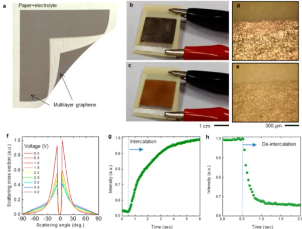
Figure 1summarizes the optical and electrical properties of ML-graphene-on-paper. We synthesized ML-graphene on Ni foils using a chemical vapor deposition system using methane as a carbon source. After the growth, we etched the metal substrate that leads to a free-standing graphenefilm on water surface. By immersing the paper substrate into the liquid we managed to transfer large area ML-graphene on printing paper (Supporting Information, Figures 1 and 2). We used a piece of thick printing paper (Koehler Chamois Ivory Board, 246 g/m2) obtained from a local printing service. After the transfer process, we dried the paper at 70°C and obtained conformal graphene coating on the network offibers. Swelling of paper substrate during the transfer process and the surface roughness
Received: January 11, 2016
Published: June 1, 2016
Article
pubs.acs.org/journal/apchd5
Downloaded via BILKENT UNIV on December 23, 2018 at 11:49:44 (UTC).
limits the quality of the MLG films. Figure 1a shows a
photograph of ML-graphene on paper. Figure 1b shows a
confocal microscope image of graphene coated surface. The RMS surface roughness of the paper is around 3μm and the thickness is 300 μm (Figure 1c and Supporting Information, Figures 3−8). The scanning electron microscope image shows the rough surface consist of random network of fibers. The rough surface of paper provides an ideal Lambertian-view characteristics.Figure 1e shows the angular dependence of the scattering cross section of the paper surface (red line) and the Lambertian cosine model (black curve). The good agreement between the model and scattering data indicates the angle independent appearance of the paper surface. The graphene coated surface (Figure 1e, blue curve) yields more specular reflection than bare paper due to the metallic like nature. The characteristics of the diffuse reflectance varies from metallic-like to paper-like as the thickness of ML-graphene layer gets thinner (Supporting Information, Figure 9). At the same time, the sheet resistance of ML-graphene varies from 550 to 25Ω/sq as the number of graphene layers increases from 35 to 60 (Figure 1f). Besides it has an ideal-Lambertian view, the paper substrate yields a flexible and foldable support. Figure 1g shows the variation of resistance of ML-graphene layer after various acute folding scheme. We observed only 10% increase (Figure 1h) in the total resistance after acute folding, which yields some structural defects on graphene (see the inset inFigure 1g). The folding introduced structural defects on graphene due to tearing apart of the paper surface and fold breaks on the surface. MLG films can be bent with much larger curvatures.
Now, we would like to demonstrate electrically controlled color change of ML-graphene-on-paper. Figure 2a shows the schematic drawing of the paper device. We transferred ML-graphene on both side of the paper which is soaked with ionic liquid electrolyte. We used a silver-based conductive paint to make electrical contacts on graphene. Figure 2b,c shows the
photographs of the fabricated device at different bias
conditions. When we applied a bias voltage larger than 3 V, we observed a significant change in the color.Figure 2d,f shows the corresponding optical microscope image of the edge of ML-graphene. Initially, ML-graphene has a shiny metallic appearance; when we applied a voltage (>3 V) between the electrodes, it first got dark and then became semitransparent (seeMovie 1,Figure 2d,e). To quantify the color change, we measured the scattering cross section of graphene coated paper surface as we tuned the bias voltage from 0 to 4 V (Figure 2f). At 0 V, the device yields a significant specular reflection; however, as the voltage increases, the backscattered intensity is suppressed resulting more Lambertian view due to the underneath paper surface. The color of ML-graphene on paper can be switched between the metallic/black and semitransparent view in a few second.Figure 2g,h shows the time trace of the normalized intensity. Under a bias voltage, the anions of the ionic liquid intercalate into the graphene layers and block the interband transitions in the visible spectrum. The intercalation cycle takes relatively longer (∼4 s) than the deintercalation cycle (<0.5 s). We also observed that the discharging current is significantly larger than the charging current due the high conductivity of the intercalated electrode (Supporting Information, Figure 10). The switching speed Figure 1.Multilayer graphene on paper. (a) Photograph of multilayer graphene transferred on printing paper. (b) Confocal microscope image of the graphene-coated paper surface. The RMS surface roughness is around 3μm. (c) Confocal microscope image of the rough paper surface coated with ML-graphene. (d) Scanning electron microscope of the cross section and edge of graphene layer on paper. The bright area is due to electrostatic charging of the paper. The RMS surface roughness is around 3μm. (e) Scattering cross section at 650 nm of bare paper surface (red curve) and graphene-coated surface (blue curve). The black curve shows the Lambertian cosine model. The inset shows the scattering configuration. (f) The sheet resistance of ML-graphene-on-paper synthesized at different temperatures. (g) Variation of resistance of ML-graphene-on-paper for various folding configurations. The inset shows the structural defects formed after folding.
scales inversely with the area of the device. For a device with 3 × 3 mm2area, the response time is less than a second. The spectrum of the color change covers nearly all visible spectrum (Supporting Information, Figure 11), however, the contrast diminishes for wavelength less than 500 nm.
The profound color change is mainly because of blocking of interband transition of ML-graphene.22,26,27 The weak inter-layer coupling and very strong intrainter-layer bonding of graphene sheets allow small atoms and molecules to intercalate between the layers.28In our case, under a voltage bias, the anions of the ionic liquid intercalate into the layers and electrostatically dope
the graphene. As a result of intercalation, the charge density on graphene increases significantly and the Fermi level shifts to higher energies: about 1 eV. Unlike single layer graphene, ML-graphene has many conduction and valence subbands. The electronic transitions between these subbands result broadband absorption that can be suppressed by doping due to Pauli blocking.24To understand the mechanism of color change on paper, we performed in situ electrical and optical measure-ments.Figure 3a shows the variation of the sheet resistance of the graphene electrode during the intercalation cycle. The inset in Figure 3a shows the four-wire resistance measurement Figure 2.Electrically controlled color change on paper. (a) Schematic representation of the graphene-based electronic paper consisting of two multilayer graphene electrodes on paper substrates. The room temperature ionic liquid is soaked into the paper. (b, c) Photographs of the fabricated device under various bias voltage. (d, e) Optical microscope images of the edge of ML-graphene at 0 and 4 V, respectively. (f) Scattering cross section (at 600 nm wavelength) under bias voltages between 0 to 4 V. (g, h) Temporal behavior of the color change during intercalation and deintercalation cycles, respectively.
Figure 3.In situ electrical and optical characterization of ML-graphene on paper. (a) Variation of the sheet resistance of ML-graphene during the intercalation process as the bias voltage between the graphene electrodes varies from 0 to 4 V. The inset shows the schematic representation of the four-point measurement system. (b) Optical transmittance of graphene at different bias voltages. (c) In situ Raman spectra recorded for the ML-graphene during the intercalation of ionic liquid.
system. We slowly changed the bias voltage applied between the graphene electrodes and recorded variation of the sheet resistance. For the undoped state, the sheet resistance is around 240 Ω/sq. As the bias voltage increases, the sheet resistance decreases substantially down to a value of 10Ω/sq. This high conductivity of the intercalated ML-graphene confirms a very high level of doping and charge densities. We observed that intercalation of acceptors (anions) into the graphene is much more efficient than the donors (cations). The bottom graphene electrode (connected to lower voltage) does not yield a visible color change. We estimate that the shift in Fermi energy is around 1.2 eV, which yields a broad optical transmittance window. The window is defined by the cutoff of Pauli blocking (2EF) and plasma frequency due to the free carriers
27,29 (ω = ε ∞ Ne m p 2 2
, where N is the carrier concentration, m is the effective mass, e is the elementary charge, and ε is the dielectric constant). Increasing carrier concentration results in a plasma frequency near the visible spectrum. As a result of these two opposite effects, the transmittance spectrum shows a broad peak centered at the plasma frequency of the ML-graphene. Figure 3b shows the spectrum of the optical transmittance at different voltages (Supporting Information, Figure 12). The transmittance of the ML-graphene electrode reaches up to 90% at 820 nm. The energy of the transmittance maxima yields a plasma frequency of 1.5 eV. We also recorded in situ Raman spectra of the ML-graphene during intercalation (Figure 2f).
We observed a significant enhancement and blue-shift in G-band (around 43 cm−1), whereas the intensity of the 2D-band diminishes. The upshift in the frequency of G-band is due to
the difference in the force constants arising from the
intercalated environment. The upshift of 43 cm−1 indicates acceptor intercalation of stage-1, which means anions intercalated into all layers. We do not observe a doublet structure, which is a characteristic behavior of partially intercalated graphitic compounds. The appearance of the D-band demonstrates the formation of defects during the intercalation process. These results reveal a very efficient and reversible intercalation process, thus, a high level of doping of graphene layers. Our results suggest that ML-graphene-on-paper can be used as an electrically reconfigurable optical material that yields a substantial color change in the visible spectra.
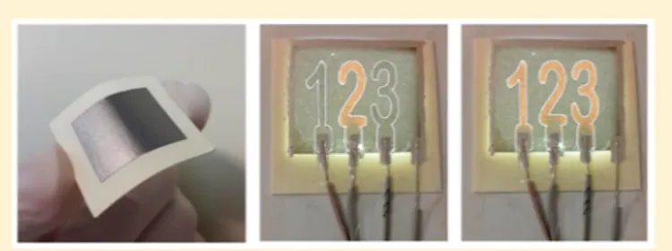
Cutting, folding, and printing are common processes for paper, but not for optical materials. Combining these scalable methods with our paper devices opens new possibilities for novel optoelectronic devices. To show the promises of this approach, we would like to demonstrate various device strategies. Thefirst design is a planar display device consisting of patterned MLG electrodes. We transferred MLG on one side of the paper and patterned the graphene electrode into individually addressable shapes (i.e., numbers) using a computer-controlled cutter. Figure 4a,b illustrates the layout Figure 4. Planar, 3D, and colored display devices on paper. (a) Schematic drawing of the planar paper display fabricated by patterning MLG electrode into isolated elements using a plotter. (b) Photograph of the operating device. The color of the isolated elements can be controlled individually. (c) 3D paper display fabricated by folding the planar paper device into three dimensions. The display elements are patterned on planar device. (d) Photograph of the operating device with back illumination. The multilayer graphene electrode preserve its electrical continuity after the folding. (e) Schematic drawing of the color device formed by printing halftone color toner on paper sandwiched between two ML-graphene electrodes. (e, f) Photograph of the working device at 0 and 4 V bias voltage.
and the photograph of the operating device with a back illumination (seeMovie 2andSupporting Information, Figures
13−15). The isolated elements and the rest work as the
coplanar electrodes. The color of each element can be switched under a voltage bias of 4 V. We observed that the performance of the coplanar devices are similar to the devices with double electrodes. The device can operate even after we crumbled up the paper substrate (Supporting Information, Figure 16).
Folding a planar paper device into three dimensions enables new 3D display devices.Figure 4c shows the folding scheme for
3D paper display. We first pattered the number-shaped
elements on the planar device then folded the substrate. Folding yields mountains and valleys on the surface and display elements on the planar faces. Figure 4d shows the picture of operation of the folded device. The graphene electrode preserves electrical continuity over the device even after many folding cycles. Furthermore, printing toner on paper allows us to add new functionality to our display devices. We demonstrated a color principle by simply printing color toner on the paper. Under a voltage bias, the graphene electrode gets transparent and the printed color appears.Figure 4e shows the schematic of the device. We printed a mosaic pattern using halftone color. Halftone colors consisting of separated dots which allow ions to intercalate the graphene electrode. Under the voltage bias, graphene gets transparent and makes the color pattern on the paper visible.Figure 4f shows the photograph of the device at 0 and 4 V bias voltages. Red, yellow, and green colors can be seen clearly trough the doped ML-graphene layer (Supporting Information, Figure 17). However, the blue dots
on the paper do not appear due to the inefficient optical
modulation.
Now, we would like demonstrate a multipixel paper display. Figure 5a shows the schematic drawing of the 5× 5 multipixel device formed by two patterned ML-graphene electrodes registered in perpendicular directions. Figure 5b shows the
completed device with the wiring to the external control electronics. To address a pixel, we used passive matrix addressing by applying various bias voltage of 0, 2, and−2 V to the rows and columns. When we applied 2 V to a column and−2 V to a row, the color of the intersecting area changes from metallic to paper-view. Using a manual switch box, we were able to reconfigure the pattern by manually adjusting the voltage configuration.Figure 4b shows the images of the device with different reconfigurable patterns (seeMovie 3for the real-time operation). The migration of the boundary of the color change illustrates the intercalation process. We were able to
reconfigure the pattern on paper many times; however, we
observed that after 30 min or voltages larger than 5 V, the graphene layer gets oxidized and turns into a dark back color that cannot be reversed. Degradation of the performance is likely due to the very reactive nature of highly doped graphene in air. The water content in ionic liquid is another detrimental factor on graphene. Undoped graphene is very stable in air; however, highly doped graphene can be oxidized in ambient conditions. To reduce the oxidation, wefirst tested our device in vacuum. We observed that we can apply more voltages (>5 V) and the device can provide a similar color change. Coating the surface of graphene with a thin polymer layer improves the stability (seeSupporting Information, Figure 18). Our results suggest that the degradation of the device performance is due to oxygen in the atmosphere and water content in the electrolyte. The durability of the device increases when we bake the ionic liquid in vacuum before we inject it into the paper.
In the final section we would like to demonstrate
compatibility of our method with roll-to-roll fabrication processes that play a key role for paper-based substrates. We modified our CVD system to handle large nickel foils. We grew multilayer graphenefilms at 1000 °C on large area nickel foils by continuously moving the foil inside the chamber along the hot zone.Figure 6a summarizes the continuous CVD process of Figure 5. Multipixel paper display. (a) Schematic representation of multipixel paper display using 5× 5 array of patterned MLG electrodes transferred both side of the paper is a cross bar structure. The width and the length of graphene electrodes are 5 mm and 2.5 cm, respectively. (b) Photograph of the fabricated paper display with the attached wiring. (c) Photograph of the reconfigurable pattern on paper display using passive matrix addressing at various voltage configurations controlled by an electronic switch box.
MLG. Since the thickness of MLG is defined by the growth temperature rather than growth time, homogeneity of the temperature inside the chamber is a key parameter for the
continuous growth. After the growth, we first tested the
scalability of the transfer technique. Withfishing technique, we were able to transfer MLG with size up to 6″ in diagonal. Larger sample size results in large cracks during the transfer process, which preventsfishing methods for roll-to-roll process. Then we tested hot lamination-based transfer processes. We partially coated the surface of the paper with a very thin layer of thermal adhesive, and then we laminated MLG-coated nickel foils on the paper surface. The partial coating is enough to hold the MLGfilm on the paper surface, and it allows penetration of ions. After etching the nickel foil, we obtained crack-free, large-scale MLG films on paper (Figure 6c). The hot lamination technique and chemical etching is fully compatible with roll-to-roll processes.
We have shown that multilayer graphene on paper can be used as an electrically reconfigurable medium for display applications. In our device, graphene layers operates as both electrode and the optically active layer. The paper substrate providesflexible and foldable mechanical support which holds the electrolyte. Intercalation of multilayer graphene electrodes with room temperature ionic liquid yield high contrast reconfigurable color change on a piece of printing paper. Scalable processing techniques used for paper manufacturing, such as cutting, folding, or printing, enable us to demonstrate novel paper-based optoelectronic devices that cannot be realized with wafer-based techniques. We anticipate that our results provide a significant step for realization of low-cost, disposable (Supporting Information, Figure 19), and ubiquitous optoelectronics on unconventional substrates.
■
METHODS SUMMARYSynthesis of Multilayer Graphene. Multilayer graphene samples were synthesized on 50μm thick nickel foil substrates
(Alfa Aesar item #12722) using chemical vapor deposition
system. The thickness of ML graphene samples were controlled by the growth temperatures varied between 900 and 1000°C. As the carbon feedstock, we used 30 sccm of CH4gas at the ambient pressure during the growth. To remove the oxide layer on Ni substrate, we anneled the samples under a flow of 100 sccm Ar and 100 sccm H2gases at 950°C. Growth time was 5 min then the samples were left for fast cooling to room temperature.
Transfer-Printing of Multilayer Graphene on Paper. Transfer printing of large area ML-graphene (up to size of 15
cm) on paper substrates were done by a so-called “fishing
process”. ML graphene is detached from the nickel substrate in dense FeCl3solution (1 M), and then it was transferred on a clean water surface. Due to the hydrophobic nature of the graphene surface, MLG stays on the surface of water. Immersing the paper substrate into the liquid initiates conformal coating of the ML graphene on the paper surface. Finally, the ML graphene holding paper was dried in an oven at 70°C for 2 h to remove the water content that remains during the transfer printing procedure.
Preparation of the Graphene-on-Paper Display Devices. After transfer printing of ML graphene to both sides of the paper, we used silver-based conductive ink on opposite sides of the top and bottom ML graphene as contact electrodes. When the conductive ink was dried, 50μL of ionic liquid electrolyte [DEME][TFSI] (98.5%, diethylmethyl
(2-methoxyethyl)ammonium-bis(trifluoromethylsulfonyl)imide,
Sigma-Aldrich, 727679) injected into the paper. We attached two copper wires to apply voltage to the top and bottom ML graphene through the silver-based contact electrodes.
Scattering Cross Section Measurements. We measured the scattering cross-section from the bare and graphene-coated paper surface using a supercontinuum laser (Koheras-SuperK Versa) integrated with an acousto-optic tunable filter. The wavelength can be tuned between 450 to 650 nm with 1 nm spectral width. The incidence angle was controlled with a
motorized rotary stage with an accuracy of 0.01°. The
polarization-dependent reflection from the metal surface is detected with a photodiode (Newport 818) connected to an amplifier. During the scattering measurements, we biased the graphene-based paper displays by using Keithley 2400 source measure unit. The charging and discharging currents are also recorded simultaneously during the measurement.
Raman Spectroscopy. We used Jobin Yvon Horiba Raman microscope system with a green laser having 532 nm excitation wavelength. The open device architecture of graphene-based paper displays allowed us to measure the variations in the Raman spectrum of the ML-graphene under a bias voltage. The voltage was applied to the graphene-based paper displays by Keithley 2400 source-measure-unit.
In Situ Electrical Measurements. A four-point resistance measurement system is used to measure contact resistance of ML-graphene during intercalation and deintercalation. We used two separate source meters (Keithley 2400 and 2600) to Figure 6.Scaling up the process. (a) Schematic representation of the continuous chemical vapor deposition of multilayer graphene on Ni foils. (b) Transfer process of multilayer graphene from Ni foil to paper substrate with hot lamination. The paper surface is partially coated with a polymer adhesive which holds the graphene layer and allows penetration of the electrolyte. (c) Photograph of the multilayer graphene transferred on A4-size printing paper.
measure sheet resistance and apply bias voltage between graphene electrodes to initiate intercalation.
■
ASSOCIATED CONTENT*
S Supporting InformationThe Supporting Information is available free of charge on the ACS Publications website at DOI: 10.1021/acsphoto-nics.6b00017.
Real-time movie of the electrically controlled color change on paper (MOV).
Real-time movie of the planar paper display (MOV). Real-time movie of the multipixel paper display (MOV). Transferring ML-graphene on paper, variation of the resistance of ML-graphene under continuous folding, 3D-topography measured with an optical profiler, effect
of surface roughness of paper on MLG films,
trans-mittance and reflectance spectra of the ML-graphene on transparent PVC substrates, angular dependent normal-ized scattering cross section of paper coated with ML-graphene grown at different temperature, charging and discharging current intercalation and deintercalation cycles, stability test of the devices in vacuum, and disposable devices (PDF).
■
AUTHOR INFORMATIONCorresponding Author
*E-mail:[email protected]. Phone: +90 3122908078.
Notes
The authors declare no competingfinancial interest.
■
ACKNOWLEDGMENTSThis work was partially supported by the Scientific and
Technological Research Council of Turkey (TUBITAK) Grant No. 113F278. C.K. also acknowledges the support from the
European Research Council (ERC) Consolidator Grant ERC−
682723 SmartGraphene.
■
REFERENCES(1) Steckl, A. J. Circuits on Cellulose. IEEE Spectrum 2013, 50, 48− 61.
(2) Bauer, S. Flexible Electronics: Sophisticated Skin. Nat. Mater. 2013, 12, 871−872.
(3) Kang, S. J.; Kocabas, C.; Ozel, T.; Shim, M.; Pimparkar, N.; Alam, M. a; Rotkin, S. V.; Rogers, J. A. High-Performance Electronics Using Dense, Perfectly Aligned Arrays of Single-Walled Carbon Nanotubes. Nat. Nanotechnol. 2007, 2, 230−236.
(4) Kaltenbrunner, M.; Sekitani, T.; Reeder, J.; Yokota, T.; Kuribara, K.; Tokuhara, T.; Drack, M.; Schwödiauer, R.; Graz, I.; Bauer-Gogonea, S.; Bauer, S.; Someya, T. An Ultra-Lightweight Design for Imperceptible Plastic Electronics. Nature 2013, 499, 458−463.
(5) White, M. S.; Kaltenbrunner, M.; Głowacki, E. D.; Gutnichenko, K.; Kettlgruber, G.; Graz, I.; Aazou, S.; Ulbricht, C.; Egbe, D. a. M.; Miron, M. C.; Major, Z.; Scharber, M. C.; Sekitani, T.; Someya, T.; Bauer, S.; Sariciftci, N. S. Ultrathin, Highly Flexible and Stretchable PLEDs. Nat. Photonics 2013, 7, 811−816.
(6) Kim, R.-H.; Kim, D.-H.; Xiao, J.; Kim, B. H.; Park, S.-I.; Panilaitis, B.; Ghaffari, R.; Yao, J.; Li, M.; Liu, Z.; Malyarchuk, V.; Kim, D. G.; Le, A.-P.; Nuzzo, R. G.; Kaplan, D. L.; Omenetto, F. G.; Huang, Y.; Kang, Z.; Rogers, J. A. Waterproof AlInGaP Optoelectronics on Stretchable Substrates with Applications in Biomedicine and Robotics. Nat. Mater. 2010, 9, 929−937.
(7) Kim, D.-H.; Lu, N.; Ma, R.; Kim, Y.-S.; Kim, R.-H.; Wang, S.; Wu, J.; Won, S. M.; Tao, H.; Islam, A.; Yu, K. J.; Kim, T.; Chowdhury, R.; Ying, M.; Xu, L.; Li, M.; Chung, H.-J.; Keum, H.; McCormick, M.; Liu,
P.; Zhang, Y.; Omenetto, F. G.; Huang, Y.; Coleman, T.; Rogers, J. A. Epidermal Electronics. Science 2011, 333, 838−843.
(8) Ko, H. C.; Stoykovich, M. P.; Song, J.; Malyarchuk, V.; Choi, W. M.; Yu, C. J.; Geddes, J. B., 3rd; Xiao, J.; Wang, S.; Huang, Y.; Rogers, J. A. A Hemispherical Electronic Eye Camera Based on Compressible Silicon Optoelectronics. Nature 2008, 454, 748−753.
(9) Rogers, J. A.; Bao, Z.; Baldwin, K.; Dodabalapur, A.; Crone, B.; Raju, V. R.; Kuck, V.; Katz, H.; Amundson, K.; Ewing, J.; Drzaic, P. Paper-like Electronic Displays: Large-Area Rubber-Stamped Plastic Sheets of Electronics and Microencapsulated Electrophoretic Inks. Proc. Natl. Acad. Sci. U. S. A. 2001, 98, 4835−4840.
(10) Sia, S. Cutting Edge: Thin, Lightweight, Foldable Thermochro-mic Displays on Paper. Lab Chip 2009, 9, 2763.
(11) Comiskey, B.; Albert, J. D.; Yoshizawa, H.; Jacobson, J. An Electrophoretic Ink for All-Printed Reflective Electronic Displays. Nature 1998, 394, 253−255.
(12) Hayes, R. A.; Feenstra, B. Video-Speed Electronic Paper Based on Electrowetting. Nature 2003, 425, 383−385.
(13) Martinez, A. W.; Phillips, S. T.; Whitesides, G. M.; Carrilho, E. Diagnostics for the Developing World: Microfluidic Paper-Based Analytical Devices. Anal. Chem. 2010, 82, 3−10.
(14) Kim, D. H.; Kim, Y. S.; Wu, J.; Liu, Z.; Song, J.; Kim, H. S.; Huang, Y. Y.; Hwang, K. C.; Rogers, J. A. Ultrathin Silicon Circuits with Strain-Isolation Layers and Mesh Layouts for High-Performance Electronics on Fabric, Vinyl, Leather, and Paper. Adv. Mater. 2009, 21, 3703−3707.
(15) Felton, S.; Tolley, M.; Demaine, E.; Rus, D.; Wood, R. A Method for Building Self-Folding Machines. Science 2014, 345, 644− 646.
(16) Andersson, P.; Nilsson, D.; Svensson, P. O.; Chen, M.; Malmström, A.; Remonen, T.; Kugler, T.; Berggren, M. Active Matrix Displays Based on All-Organic Electrochemical Smart Pixels Printed on Paper. Adv. Mater. 2002, 14, 1460−1464.
(17) Liu, M.; Yin, X.; Ulin-Avila, E.; Geng, B.; Zentgraf, T.; Ju, L.; Wang, F.; Zhang, X. A Graphene-Based Broadband Optical Modulator. Nature 2011, 474, 64−67.
(18) Wang, F.; Zhang, Y.; Tian, C.; Girit, C.; Zettl, A.; Crommie, M.; Shen, Y. R. Gate-Variable Optical Transitions in Graphene. Science 2008, 320, 206−209.
(19) Mak, K. F.; Ju, L.; Wang, F.; Heinz, T. F. Optical Spectroscopy of Graphene: From the Far Infrared to the Ultraviolet. Solid State Commun. 2012, 152, 1341−1349.
(20) Nair, R. R.; Grigorenko, A. N.; Blake, P.; Novoselov, K. S.; Booth, T. J.; Peres, N. M. R.; Stauber, T.; Geim, A. K. Fine Structure Constant Defines Visual Transparency of Graphene. Science 2008, 320, 1308.
(21) Gan, X.; Shiue, R. J.; Gao, Y.; Mak, K. F.; Yao, X.; Li, L.; Szep, A.; Walker, D.; Hone, J.; Heinz, T. F.; Englund, D. High-Contrast Electrooptic Modulation of a Photonic Crystal Nanocavity by Electrical Gating of Graphene. Nano Lett. 2013, 13, 691−696.
(22) Hennig, G. R. Optical Transmission of Graphite Compounds. J. Chem. Phys. 1965, 43, 1201.
(23) Bao, W.; Wan, J.; Han, X.; Cai, X.; Zhu, H.; Kim, D.; Ma, D.; Xu, Y.; Munday, J. N.; Drew, H. D.; Fuhrer, M. S.; Hu, L. Approaching the Limits of Transparency and Conductivity in Graphitic Materials through Lithium Intercalation. Nat. Commun. 2014, 5, 4224.
(24) Polat, E. O.; Balcı, O.; Kocabas, C. Graphene Based Flexible Electrochromic Devices. Sci. Rep. 2014, 4, 6484.
(25) Polat, E. O.; Kocabas, C. Broadband Optical Modulators Based on Graphene Supercapacitors (Supplementary). Nano Lett. 2013, 13, 5851−5857.
(26) Skulason, H. S.; Gaskell, P. E.; Szkopek, T. Optical Reflection and Transmission Properties of Exfoliated Graphite from a Graphene Monolayer to Several Hundred Graphene Layers. Nanotechnology 2010, 21, 295709.
(27) Dresselhaus, M. S.; Dresselhaus, G. Intercalation Compounds of Graphite. Adv. Phys. 1981, 30, 139−326.
(28) Dresselhaus, M. S. Intercalation In Layered Materials. MRS Bull. 1987, 12, 24−28.
(29) Eklund, P. C.; Smith, D. S.; Murthy, V. R. K. Optical Reflection Studies of the Electronic Properties of Stages 2− 5 Graphite-SbCl5.
Synth. Met. 1981, 3, 111−122.