Double doping synergy to improve structural, morphological, optical,
and electrical properties of solution‑based Cd and M (M: Pb, Sn, Bi)
double doped nanocrystalline copper oxide films
Bunyamin Sahin1 · Rasit Aydin2
Received: 7 March 2019 / Accepted: 3 November 2019 / Published online: 12 November 2019 © Springer-Verlag GmbH Germany, part of Springer Nature 2019
Abstract
In this study, nanostructured CuO, Cd0.01Cu0.99O and Cu0.98Cd0.01M0.01O (M: Pb, Bi, Sn) films were synthesized using the successive ionic layer adsorption and reaction technique. The effects of Cd-doping, Sn, Pb, and Bi double doping on the structural, morphological, optical, and electrical properties were systematically investigated via X-ray diffraction (XRD), scanning electron microscopy (SEM), UV–Vis spectroscopy, and current–voltage (I–V) measurements, respectively. XRD results show that the peak intensity, crystallite size, and texture coefficient of the films changed intensely with double doping. SEM images reveal that the surface morphology of the nanostructures changed with the kind of dopant materials due to the differences in ionic radius. Energy dispersive X-ray spectroscopy studies confirmed the presence of Cd2+, Sn4+, Pb2+, and
Bi+5 in the doped films. The estimated average optical band gap energies of the CuO samples varied from 1.366 to 1.480 eV
with double doping. The lowest average electrical resistivity of 1.21 × 10⁶ Ω cm was found for the Bi
0.01 Cd0.01Cu0.98O sample.
1 Introduction
Nanostructured transition metal oxide semiconductor materi-als (MOs) such as zinc oxide (ZnO), nickel oxide (NiO), and titanium dioxide (TiO2) [1–3] have created a good deal of interest, because of their diverse applications as gas sensors, fuel cells, solar cells, and light emitting diodes in electronic and optoelectronic devices [4–6]. Among the different metal oxide materials, there are two different stable copper oxide states according to oxygen combination. In the oxides of copper category, cuprous oxide (Cu2O) with cubic phase and
cupric oxide (CuO) with monoclinic phase are the preferred metal oxides to obtain films with several structures. Cop-per oxide is a monoclinic structure p-type transition metal oxide material. Copper vacancies cause narrowing of the band gap and the semiconductor to become a p-type mate-rial with a high melting temperature of 1200 °C, constricted
band gap energy of ~ 1.4 eV and density of 6.31 g/cm3 [7, 8].
Compared to the different n-type MOs materials, band gap values of CuO are between 1.2 and 2.1 eV [8, 9], which is appropriate for solar energy converting systems. Transition copper oxide films have been broadly implemented, because of their numerous advantages such as being environmental-friendly [10], cost-effective, chemically stable, abundant in nature, and easy to process [11]. Due to its excellent proper-ties, CuO is used for many technological implementations such as solar cells [12], gas sensors [13], antimicrobial and anticancer activities [14], nanodevices for catalysis, and thin film transistors [15].
CuO nanostructured films have been developed in dif-ferent ways such as pulsed laser deposition [16], the solu-tion combussolu-tion method [17], thermal evaporation [18], the flame spray pyrolysis method [19], and successive ionic layer adsorption and reaction (SILAR) [20]. Among the different methods of synthesis, the SILAR technique is a suitable solution for good-quality nanostructured CuO films since it is a low temperature [21], simple [22], and inexpen-sive method [23].
Doping is a very powerful approach to enhance the physi-cal performance of nanostructured CuO films. Different alkali metals such as Li and Na, transition metals like Mn, Zn, and Co and basic metals such as Sn and Pb have been explored as dopant materials [24–27]. It has been reported
* Bunyamin Sahin [email protected]
1 Laboratory of Nanostructured Materials and Applications,
Faculty of Arts and Sciences, Mustafa Kemal University, Hatay, Turkey
2 Department of Physics, Faculty of Sciences, Selcuk
that Cd-doped metal oxides are a promising material for applications in optoelectronic device technology [28–30]. Furthermore, it has been shown that Cd substitution leads to an increase in crystalline quality and reduces the disloca-tion density [29, 31]. Also, it has been reported that double doping drastically alters the main physical quantity of metal oxides [32–35].
In the literature, no research has been reported on the deposition of nanostructured Cu0.98Cd0.01M0.01O (M: Pb,
Bi, Sn) films using the SILAR technique. Consequently, in the present study, an approach has been made to properly explore the structural, morphological, optical, and electri-cal properties and their correlation with double doping of (Cd + Sn) (Cd + Pb) and (Cd + Bi). We used the SILAR method to grow CuO, Cd0.01Cu0.99O and Cu0.98Cd0.01M0.01O
(M: Pb, Bi, Sn) nanostructures that to the best of our knowl-edge have not been decelerated before. It was observed that double doping of Sn4+, Pb4+ and Bi5+ ions by Cd2+ ions
strongly affects the structural, surface morphological, opti-cal, and electrical properties of CuO nanostructures.
2 Materials and methods
2.1 Materials
Copper (II) chloride dehydrate (CuCl2·2H2O), cadmium
ace-tate dihydrate [Cd(COOCH3)2·2H2O], bismuth (III) chloride
(BiCl3), lead (II) acetate trihydrate [Pb(CH3CO2)2·3H2O],
tin (II) chloride (SnCl2), acetone (CH3COCH3), ammonium hydroxide (NH4OH), and sulfuric acid solution (H2SO4)
were obtained from commercial dealers.
2.2 Synthesis of CuO thin films
CuO, Cd0.01Cu0.99O and Cu0.98Cd0.01M0.01O (M: Pb, Bi,
Sn) thin films were prepared by the SILAR method on soda lime glass substrates (76 × 26 mm). To procure the precursor solution, 1.7 g CuCl2·2H2O was mixed with 100 ml double
distilled water, which resulted in a 0.1 M copper (II) chloride solution. To examine the effect of the doping in the growth solution, Cd and (Cd + Bi) (Cd + Pb), and (Cd + Sn) were added to each solution. The pH value of the solution was increased to ≈ 10.0 by adding ammonium hydroxide and the solution was heated to about 85 °C. The doped CuO precursor solutions were synthesized by adding 1 M% each of dopants cadmium, bismuth, lead and tin, respectively. For the SILAR process, the pre-cleaned glass substrate was first dipped in copper (II) chloride dihydrate solution for 20 s. Then, the substrate was immersed in DI water for 20 s to deport any weakly attached ions. These cycles were repeated six times. Then, the as-grown CuO films were annealed in air conditioned at 350 °C for 1 h.
2.3 Characterization of CuO films
The structural investigations of the CuO films were made using X-ray diffraction (Bruker D8 Advance X-ray dif-fractometer) with a high-intensity Cu Kα radiation (λ = 0.15406 nm). The general surface properties of CuO films were examined by scanning electron microscope (SEM) (Zeiss EVO LS 10) and compositional analysis by EDS with attached SEM. The optical absorbance data were obtained using a Thermo Scientific Genesys 10S UV–Vis spectrophotometer. The electrical resistivity of CuO films was obtained using the four-point probe method at room temperature with a Keithley pico ampere meter.
3 Results and discussion
3.1 Crystal structure
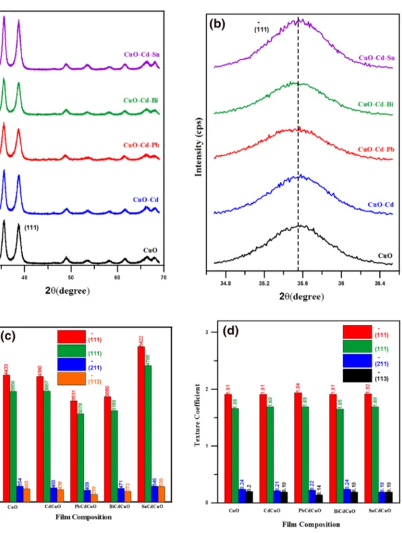
XRD examinations were performed to define the crystal phase, as well as the particle size and growth orientation of the CuO films; XRD patterns were recorded and are shown in Fig. 1a. This shows the X-ray diffraction patterns of CuO, Cd0.01Cu0.99O and Cu0.98Cd0.01M0.01O (M: Pb, Bi, Sn) films
grown on glass substrates under identical conditions. The XRD patterns show that the growth of host CuO films was ( 111 ) and ( 111 ) was the preferred orientation (JCPDS card no. 05-0640). All the double doped CuO films show an intense ( 111 ) and ( 111 ) preferential orientation like that of the Cd0.01Cu0.99O and CuO films. The peak intensity change was observed in the X-ray diffraction pattern for the CuO material, which implies the variation of the lattice param-eter [36, 37]. Figure 1b presents the enlarged patterns of the peaks at about 2θ = 35.45°, corresponding to the 111 planes of nanostructured CuO. As is recognized, the lattice parameter is strongly interconnected with the ionic radii of metals [Cu = 0.73 Å, Cd = 0.95.Å, Sn = 0.69 Å, Pb = 1.19 Å, and Bi = 0.76 Å (for six-coordination number)] [38]. The obtained change here might be owing to the differences in ionic radii between the dopant ions and host ions as shown in Fig. 1c [39, 40]. The determined change can be attributed to the attractive force of the oxygen ions and Cd, Sn, and Bi ions. Hence, the rivalry between Coulomb forces and ionic radii is responsible for the determined change of the crystal-line structure [41, 42]. This result indicates the successful introduction of dopant atoms into the CuO host lattice with no effect on the structure of CuO. As a consequence of dop-ing, the peak intensity is changed and none of the pure CuO peaks disappeared for the doped samples.
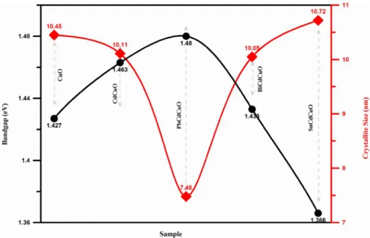
The estimated crystallite size (D) for the CuO films was determined by applying the Scherrer equation [22] and
found to vary in the range 7.48–10.72 nm with the type of dopant materials.
(1)
D= 0.94𝜆 𝛽cos 𝜃,
where D is the crystallite size weighted by volume, λ is the wavelength of the radiation (0.154 nm), and β is the integral breadth of the peak at the Bragg’s angle θ. The estimated size values for ( 111 ) ( 111 ) ( 202 ) and ( 113 ) planes are pre-sented in Table 1.
Fig. 1 a XRD patterns of CuO, Cd0.01Cu0.99O and Cu0.98Cd0.01M0.01O
(M: Pb, Bi, Sn) films. b Magnified XRD patterns of ( 111) plane of CuO, Cd0.01Cu0.99O and Cu0.98Cd0.01M0.01O (M: Pb, Bi, Sn) films. c
The relative peak intensities for (
111) (111), (211) , and (113) plane
of CuO, Cd0.01Cu0.99O and Cu0.98Cd0.01M0.01O (M: Pb, Bi, Sn) films.
d The texture coefficient for (
111) (111), (211) , and (113) plane of CuO, Cd0.01Cu0.99O and Cu0.98Cd0.01M0.01O (M: Pb, Bi, Sn) films
The texture coefficient (TC) of the plane indicates the tex-ture of a specific plane, whose deflection from the standard sample signifies the preferred growth. Equation (2) is used to obtain the preferential orientation factor of ( 111 ) ( 111 ) ( 202 ) and ( 113 ) values of the CuO films [22]. The obtained preferential orientation factor values are listed in Table 2.
The ( 111 ) and ( 111 ) preferential growth noticed for the CuO, Cd0.01Cu0.99O and Cu0.98Cd0.01M0.01O (M: Pb, Bi, Sn) samples can be observed and are exhibited in Fig. 1d. This difference is a consequence of the differences in ionic radii between substituent ions and host ion Cu2+.
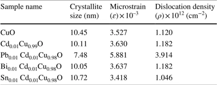
The other microstructural parameters such as microstrain (𝜀) and dislocation density (𝜌) of the nanostructured CuO films were computed via consequent Eqs. (3) and (4) [22], respectively. The computed structural parameters are shown in Table 1.
where ɑ is the lattice constant and (ρ) is the dislocation den-sity. The dislocation density was observed to decrease from 1.12 to 1.046 with Cd + Sn doping. The obtained values have (2) TC(hkl)= I(hkl)∕I0(hkl) N−1∑ NI(hkl)∕I0(hkl) . (3) (𝜀) =𝛽cos 𝜃 4 (4) (𝜌) = 15𝜀 aD,
opposite behavior to the crystallite size calculations. This opposite correlation between the average crystallite size, microstrain, and dislocation density is plotted in Fig. 2. A similar outcome is to be found in the literature [43, 44].
From this result, the increase in the estimated crystallite size and decrease in dislocation density imply that there is an enhancement in crystalline quality with double doping as a consequence of the recrystallization process [45, 46].
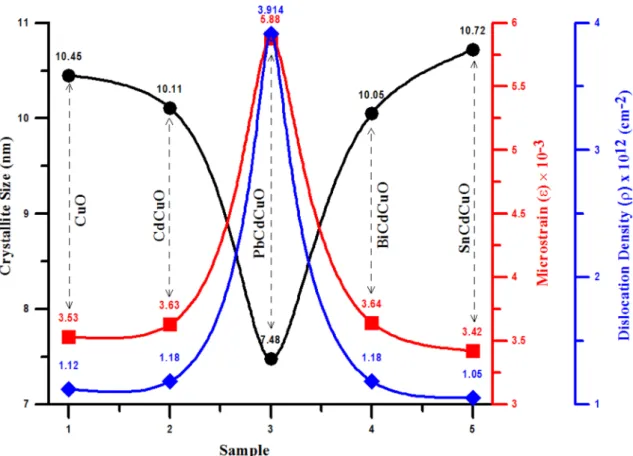
3.2 Morphological properties and EDS analysis
An analysis of the surface morphological properties of metal oxide films is critical for the discovery of their optoelec-tronic properties. Hence, it is very important to investigate the surface morphology effects of metal oxide films. The surface morphological properties of CuO, Cd0.01Cu0.99O and Cu0.98Cd0.01M0.01O (M: Pb, Bi, Sn) films were investigated
using SEM. The obtained SEM micrographs of these nano-structured CuO materials are illustrated in Fig. 3.
As can be seen from the SEM images, the doping process severely influences surface morphology of the CuO films. The changes in surface properties are attributed to differ-ences in the ionic radii of doping elements. As indicated by the varied ionic radii of dopant elements, these dopant mate-rials substitute for Cu2+ ions in the crystal lattice structure
of CuO films. The surface properties of the Cd0.01Cu0.99O
and Cu0.98Cd0.01M0.01O (M: Pb, Bi, Sn) films were affected by dopant elements due to the changed compressive stress in the CuO films caused by the difference in the ionic radii of elements. Besides, the changes in surface morphologies may be attributed to the electronegativity difference between the dopant (Cd2+, Sn4+, Pb2+ and Bi5+) and (Cu2+, O2−) host
elements. The electronegativities of Cu2+, Cd2+, Sn4+, Pb2+,
and Bi5+ were 1.19, 1.69, 1.96, 2.33, and 2.02, respectively
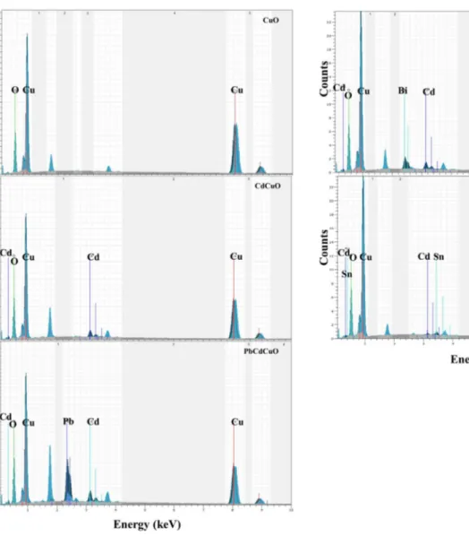
[45, 47]. The elemental composition analyses of CuO films were specified by EDS analysis. The EDS images of the nanostructured CuO films synthesized by SILAR are shown in Fig. 4.
As can be seen in Fig. 4, undoped CuO has only Cu (47.27 at. %) and O (52.73 at. %) elements. It can be clearly seen that undoped CuO films show no proof of the existence
Table 1 Estimated crystallite size, microstrain, dislocation density, band gap, and resistivity values of CuO films
Sample name Crystallite
size (nm) Microstrain(ɛ) × 10–3 Dislocation density (ρ) × 1012 (cm−2)
CuO 10.45 3.527 1.120
Cd0.01Cu0.99O 10.11 3.630 1.182
Pb0.01 Cd0.01Cu0.98O 7.48 5.881 3.914
Bi0.01 Cd0.01Cu0.98O 10.05 3.637 1.182
Sn0.01 Cd0.01Cu0.98O 10.72 3.418 1.046
Table 2 Relative peak intensity and Tc(hkl) values
of CuO, Cd0.01Cu0.99O and
Cu0.98Cd0.01M0.01O (M: Pb, Bi,
Sn) films
Sample name Relative peak
Intensity (cps) Tc(hkl) (111) (111) (111) (111) (202) (113) CuO 4433 3856 1.91 1.66 0.24 0.20 Cd0.01Cu0.99O 4380 3867 1.91 1.69 0.21 0.19 Pb0.01 Cd0.01Cu0.98O 3531 3078 1.94 1.69 0.22 0.14 Bi0.01 Cd0.01Cu0.98O 3680 3189 1.91 1.65 0.24 0.19 Sn0.01 Cd0.01Cu0.98O 5422 4766 1.92 1.69 0.19 0.19
of Cd, Sn, Pb, and Bi ions, whereas these ions exist on the surfaces of the Cd0.01Cu0.99O and Cu0.98Cd0.01M0.01O (M:
Pb, Bi, Sn) films as is clearly exhibited on the EDS micro-graphs (Fig. 4). The composition of the elements Cu, Cd, Sn, Pb, and Bi are compiled in Table 3.
3.3 Optical studies
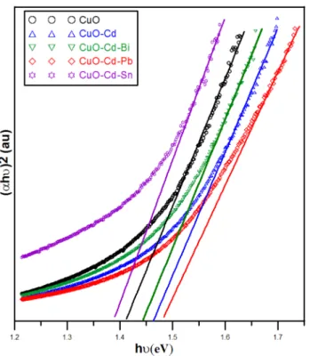
Variations in the absorption were performed at room tem-perature. The optical band gap energies of nanostructured CuO films were obtained via the optical absorption spectra. For the calculation of the average optical band gap energy values of the films, we used the prevalent Tauc’s law [22]
where α is the absorption coefficient and hν is the inci-dent photon energy. Eg is the optical band gap energy and
m depends upon the transition of carriers. (For directly
per-mitted transitions m is ½). We plotted (αhν)2 against the
photon energy (hv) for both the undoped and doped CuO thin films. The plots of (αhν)2 against (hν) for the CuO films
exhibited in Fig. 5 give the value of average direct band gap (5)
𝛼h𝜈= C(h𝜈 − Eg)m,
energy (Eg) of 1.427 eV for undoped CuO; 1.463 eV for Cd0.01Cu0.99O; 1.48 eV for Pb0.01 Cd0.01Cu0.98O; 1.433 eV for
Bi0.01 Cd0.01Cu0.98O; and 1.366 eV for Sn0.01 Cd0.01Cu0.98O
as shown in Table 4. It can be understood that the average optical band gap energy for Cd0.01Cu0.99O films (1.463 eV) is enlarged when compared to undoped CuO film. The optical band gap energy of CdO (about Eg = 2.40 eV) is higher than
that of undoped CuO (1.427 for this research). The opti-cal band gap of Cd0.01Cu0.99O should be higher than that of undoped CuO films.
Comparing our obtained optical band gap results for Cd0.01Cu0.99O and Cu0.98Cd0.01M0.01O (M: Pb, Bi, Sn) thin films with the undoped CuO films, we observed serious alterations in the average optical band gap energy values, which could be explained by the crystallite size of the undoped film that differs from the doped films in as much as it influences the absorbance and transmittance properties of materials [48]. Meanwhile, there is a strong relationship between the average optical band gap energy and grain size (quantum size effect) [49, 50]. The size effect causes the amplification of the average optical band gap energy at small crystallite sizes. This is exhibited in Fig. 6 and has also been reported by other investigators [51, 52]. The variation in
the average optical band gap may be attributed to the sur-face morphological alterations of the films, which changes atomic distances and particle size in the films [53, 54]. These consequences are additionally consistent with the SEM results, where the particle size changes with double doping. Another possible reason may be the existence of defects in the doped CuO crystal structure as a consequence of differ-ent dopant elemdiffer-ents leading to a slight shift in the average optical band gap energy.
This change, also recorded in the literature, can be con-solidated with the improvement of the metal oxide band gap as a result of the Burstein–Moss effect in the case of differ-ent dopant elemdiffer-ents [55]. The change in the average optical band gap of CuO films after different metal doping is as a consequence of the replacement of interstitial copper ions in the CuO lattice by dopant ions. Such dopant ions would present some additional energy levels in the CuO band gap close to the valence band edge [56]. Another justification for the average optical band gap change is probably owing
to photon absorption shifts toward the blue, as a result of a larger extended localization in the conduction and valence bands [55, 57].
3.4 Electrical properties
Doping and double doping can also modify the electrical features of CuO films. For this reason, to examine the electri-cal attributes of CuO, Cd0.01Cu0.99O and Cu0.98Cd0.01M0.01O (M: Pb, Bi, Sn) samples, their average electrical resistivity was found at room temperature using the linear four-point probe method. Figure 7 and Table 4 depict the alteration in average resistivity as a function of Pb, Bi, and Sn dopant elements in nanostructured CuO films.
The values of average resistivity were specified to be 7.13, 0.80, 7.28, 1.21, and 5.79 (106 Ω cm) for undoped, Cd-doped (Cd0.01Cu0.99O), and Cd + M double doped [Cu0.98Cd0.01M0.01O (M: Pb, Bi, Sn)] CuO nanostructures,
respectively. From Fig. 7 and Table 4, it can be observed that
Fig. 3 SEM images of CuO, Cd0.01Cu0.99O and
Cu0.98Cd0.01M0.01O (M: Pb, Bi,
the doping of Cd2+ ions and double doping of (Cd2+, Pb4+)
(Cd2+, Bi5+), and (Cd2+, Sn4+) double ions into CuO lattice
cause a change in average electrical resistivity. The vari-ance of average resistivity may arise from the replacement of Cu2+ ions by Cd2+ ions and (Cd2+, Pb4+), (Cd2+, Bi5+),
and (Cd2+, Sn4+) double ions in the CuO matrix [58, 59].
4 Conclusions
As a conclusion, we employed the SILAR technique to prepare CuO, Cd0.01Cu0.99O and Cu0.98Cd0.01M0.01O (M: Pb, Bi, Sn) films. The influences of Cd2+, Sn4+, Pb2+, and
Bi+5 incorporation on the main physical features of CuO
Fig. 4 EDX elemental analysis of CuO, Cd0.01Cu0.99O and Cu0.98Cd0.01M0.01O (M: Pb, Bi, Sn) films
Table 3 Elemental composition of CuO, Cd0.01Cu0.99O and
Cu0.98Cd0.01M0.01O (M: Pb, Bi,
Sn) films
Sample name Cu (at%) O (at%) Cd (at%) Pb (at%) Bi (at%) Sn (at%)
CuO 47.27 52.73 – – – –
Cd0.01Cu0.99O 42.53 55.80 1.67 – – –
Pb0.01 Cd0.01Cu0.98O 40.76 53.37 2.76 3.11 – –
Bi0.01 Cd0.01Cu0.98O 51.61 45.16 1.68 – 1.55 –
films were researched. The XRD patterns and SEM results show that Cd2+, Sn4+, Pb2+, and Bi+5 atoms were
success-fully introduced into the CuO host lattice with no effect on the structure of CuO. The estimated crystallite size of the CuO samples varied from 7.48 to 10.72 nm according to
the type of dopant material. The obtained microstrain and dislocation density values showed opposite behavior to the crystallite size calculations. Microstrain and dislocation density values have an important impact on the efficiency of metal oxide-based solar cells. Due to changes in dislo-cation density, the surface recombination velocity changes, which results in a change in solar cell efficiency. The lowest dislocation density value was obtained when the CuO film was double doped with 1 M% of Cd and Sn. The average optical band gap energy was determined by Tauc’s method and found to be 1.427, 1.463, 1.480, 1.433, and 1.366 eV CuO, Cd0.01Cu0.99O and Cu0.98Cd0.01M0.01O (M: Pb, Bi, Sn) films at room temperature, respectively. The Cd doping and Cd + M (M: Pb, Bi, Sn) double doping in CuO films affects the average electrical resistivity. A minimum electrical resis-tivity of 1.21 × 10⁶ Ω.cm was measured when the CuO film
was double doped with 1 M% of Cd and Bi. Given that the band gap can be collimated to the visible region by different dopant materials, nanostructured CuO films could be use-ful in optoelectronic applications. Based on the obtained structural, morphological, optical, and electrical results, Cd0.01Cu0.99O and Cu0.98Cd0.01M0.01O (M: Pb, Bi, Sn) films
can be the promising candidates as affordable materials for photovoltaic applications like solar cell devices and light emitting diodes.
Fig. 5 The optical band gap energy values of CuO, Cd0.01Cu0.99O and
Cu0.98Cd0.01M0.01O (M: Pb, Bi, Sn) films
Table 4 To analyze the band gap and resistivity variations as a function of dopant materials, three different points from three different parts of the CuO films analyzed in the UV–Vis
Spectrophotometer and linear four-point probe method
Sample name Band gap (eV) Average band gap
(eV) Resistivity 106(Ω cm) Average resistivity
106(Ω cm) CuO 1.41 1.427 7.11 7.13 1.44 6.95 1.43 7.35 Cd0.01Cu0.99O 1.46 1.463 0.76 0.80 1.48 0.68 1.45 0.87 Pb0.01 Cd0.01Cu0.98O 1.48 1.480 7.43 7.28 1.47 7.22 1.49 7.20 Bi0.01 Cd0.01Cu0.98O 1.44 1.433 1.12 1.21 1.42 1.29 1.44 1.24 Sn0.01 Cd0.01Cu0.98O 1.39 1.366 5.80 5.79 1.36 5.68 1.35 5.89
Acknowledgements This research has been supported by the Scientific Research Projects Unit of Selcuk University (Project No: 17703028) and Scientific Research Commission of Mustafa Kemal University (Project No.: 11500).
Compliance with ethical standards
Conflict of interest The authors declared that they have no conflicts of interest in this work.
References
1. M. Kang, S.W. Kim, H.Y. Park, J. Phys. Chem. Solids 123, 266– 270 (2018)
2. B. Sahin, T. Kaya, Microelectron. Eng. 164, 88–92 (2016) 3. T.A.N. Peiris, J.S. Sagu, Y.H. Yusof, K.G.U. Wijayantha, Thin
Solid Films 590, 293–298 (2015)
4. R. Vittal, K.-C. Ho, Renew. Sustain. Energy Rev. 70, 920–935 (2017)
5. M. Dou, M. Hou, D. Liang, W. Lu, Z. Shao, B. Yi, Electrochim. Acta 92, 468–473 (2013)
Fig. 6 Variation of band gap and crystallite size of CuO, Cd0.01Cu0.99O and
Cu0.98Cd0.01M0.01O (M: Pb, Bi,
Sn) films
Fig. 7 The electrical resistivity values of CuO, Cd0.01Cu0.99O
and Cu0.98Cd0.01M0.01O (M: Pb,
6. N. Joshi, L. F. da Silva, H.S. Jadhav, F.M. Shimizu, P.H. Suman, J.-C. M’Peko, M.O. Orlandi, J.G. Seo, V.R. Mastelaro, O.N. Oliveira Jr: Sens. Actuators B 257, 906–915 (2018)
7. T. Jan, J. Iqbal, U. Farooq, A. Gul, R. Abbasi, I. Ahmad, M. Malik, Ceram. Int. 41, 13074–13079 (2015)
8. A. Tombak, M. Benhaliliba, Y.S. Ocak, T. Kiliçoglu, Results Phys. 5, 314–321 (2015)
9. K. Padrón, E.J. Juárez-Pérez, F. Forcade, R. Snyders, X. Noirfal-ise, C. Lazaa, J. Jiménez, E. Vigil, Thin Solid Films 660, 386–390 (2018)
10. Y. Akaltun, Thin Solid Films 594, 30–34 (2015) 11. B. Sahin, T. Kaya, Appl Surf Sci 362, 532–537 (2013)
12. S.M. Abbas, S.T. Hussain, S. Ali, F. Abbas, N. Ahmad, N. Ali, Y. Khan, J. Alloys Compd. 574, 221–226 (2013)
13. W. Maeng, S.H. Lee, J.D. Kwon, J. Park, J.S. Park, Ceram. Int. 42, 5517–5522 (2016)
14. A.M. El Sayed, M. Shaban, Spectrochim. Acta Part A 149, 638– 646 (2015)
15. Y.-Y. Yu, W.-C. Chien, Y.-J. Wang, Thin Solid Films 618, 134– 140 (2016)
16. P. Chand, A. Gaur, A. Kumar, U.K. Gaur, Appl. Surf. Sci. 307, 280–286 (2014)
17. M. Umadevi, A.J. Christy, Spectrochim. Acta Part A 109, 133–137 (2013)
18. A.D. Khalaji, K. Jafari, S.M. Rad, J. Nan. Str. 2, 505 (2013) 19. C.Y. Chiang, K. Aroh, S.H. Ehrman, Int. J. Hydrog. Energy 37,
4871–4879 (2012)
20. Y. Akaltun, M. Aslan, T. Yetim, T. Çayır, A. Çelik, Surf. Coat. Technol. 292, 121–131 (2016)
21. K. Ravichandran, P.V. Rajkumar, B. Sakthivel, K. Swaminathan, L. Chinnappa, Ceram. Int. 40, 12375–12382 (2014)
22. R. Aydin, B. Şahin, J. Alloys Compd. 705, 9–13 (2017) 23. E. Turan, M. Zor, M. Kul, A.S. Aybek, T. Taskopru, Philos. Mag.
92, 1716–1726 (2012)
24. C. Pandurangappa, B.N. Lakshminarasappa, Philos. Mag. 91, 4486–4494 (2011)
25. Y.-H. Choi, D.-H. Kim, S.-H. Hong, Sens. Actuators B 243, 262– 270 (2017)
26. R.-C. Wang, S.-N. Lin, J.-Y. Liu, J. Alloys Compd. 696, 79–85 (2017)
27. A. Yildiz, S. Horzum, N. Serin, T. Serin, Appl. Surf. Sci. 318, 105–107 (2014)
28. M.B. Amor, A. Boukhachem, A. Labidi, K. Boubaker, M. Amlouk, J. Alloys Compd. 693, 490–499 (2017)
29. C. Tan, D. Sun, D. Xu, X. Tian, Y. Huang, Ceram. Int. 42, 10997– 11002 (2016)
30. X. Zhang, H. Yang: Sens. Actuators B 173, 127–132 (2012) 31. A. Ranjitha, N. Muthukumarasamy, M. Thambidurai, Dhayalan
Velauthapillai, A. M. Kumar, Z.M. Gasem: Superlattices Micro-struct. 74, 114–122 (2014)
32. N. Manjula, M. Suganya, D. Prabha, S. Balamurugan, J. Srivind, V.S. Nagarethinam, A.R. Balu, J. Mater. Sci: Mater. Electron. 28, 7615–7621 (2017)
33. K. Ravichandran, R. Mohan, B. Sakthivel, S. Varadharajaperu-mal, P. Devendran, T. Alagesan, K. Pandian, Appl. Surf. Sci. 321, 310–317 (2014)
34. H. Khmissi, A.M. El Sayed, M. Shaban, J. Mater. Sci. 51, 5924– 5938 (2016)
35. A.I. Ramos-Guerra, J. Guzmán-Mendoza, M. García-Hipólito, O. Alvarez-Fregoso, C. Falcony, Ceram. Int. 41, 11279–11286 (2015) 36. M. Kaiser, J. Alloys Compd. 719, 446–454 (2017)
37. A. Yu, Y. Ma, A. Chen, Y. Li, Y. Zhou, Z. Wang, J. Zhang, L. Chu, J. Yang, X. Li, Vacuum 141, 243–248 (2017)
38. R.D. Shannon, Acta Crystallogr. A 32, 751–767 (1976) 39. P. Velusamy, R.R. Babu, K. Ramamurthi, E. Elangovan, J. Viegas,
J. Alloy. Compd. 708, 804–812 (2017)
40. E. Gürbüz, B. Şahin, Appl Phys A 124(795), 1–9 (2018) 41. G. Selvan, M.P. Abubacker, A.R. Balu, J. Mater. Sci: Mater.
Elec-tron. 28, 2335–2342 (2017)
42. F.X. Cheng, J.T. Jia, Z.G. Xu, B. Zhou, C.S. Liao, C.H. Yan, J. Appl. Phys. 86, 2727 (1999)
43. P. Kumarn, P. Sharma, A.G. Joshi, R. Shrivastav, S. Dass, V.R. Satsangi, J. Electrochem. Soc. 159, H685–H691 (2012) 44. C. Moditswe, C.M. Muiva, P. Luhanga, A. Juma, Ceram. Int. 43,
5121–5126 (2017)
45. J. Wu, K.S. Hui, K.N. Hui, L. Li, H.-H. Chun, Y.R. Cho, J. Mater. Sci: Mater. Electron. 27, 1719–1724 (2016)
46. A. Bouhdjer, A. Attaf, H. Saidi, Y. Benkhetta, M.S. Aida, I. Bou-haf, A. Rhil, Opt. Int. J. Light Electron. Opt. 127, 6329–6333 (2016)
47. A. Agrawal, T.A. Dar, P. Sen, J. Nano- Electron. Phys. 5, 02025 (2013)
48. K.O. Ighodalo, D. Obi, A. Agbogu, B.N. Ezealigo, A.C. Nwanya, S.L. Mammah, R. Bucher, M. Maaza, F.I. Ezem, Mater. Res. Bull. 94, 528–536 (2017)
49. R.C. Rodriguez, A.I. Oliva, V. Sosa, F.C. Briones, J.L. Pena, Appl. Surf. Sci. 161, 340–346 (2000)
50. S.M.H. Al-Jawad, Mater. Sci. Semicond. Process. 67, 75–83 (2017)
51. L. Sponza, J. Goniakowski, C. Noguera, Phys. Rev. B 93, 195435 (2016)
52. R. Aydin, B. Şahin, Ceram. Int. 43, 9285–9290 (2017) 53. Y. Akaltun, T. Çayır, J. Alloys Compd. 625, 144–148 (2015) 54. A. Mukherjee, B. Satpati, S.R. Bhattacharyya, R. Ghosh, P. Mitra,
Physica E 65, 51–55 (2015)
55. R.A. Mereu, A. Mesaros, M. Vasilescu, M. Popa, M.S. Gabor, L. Ciontea, T. Petrisor, Ceram. Int. 39, 5535–5543 (2013)
56. R.K. Gupta, Z. Serbetçi, F. Yakuphanoğlu, J. Alloys Compd. 515, 96–100 (2012)
57. A.D. Trolio, E.M. Bauer, G. Scavia, C. Veroli, J. Appl. Phys. 105, 113109 (2009)
58. I.B. Miled, M. Jlassi, I. Sta, M. Dhaouadi, M. Hajji, G. Mousdis, M. Kompitsas, H. Ezzaouia: J. Mater. Sci.- Mater. Electron. 29, 11286–11295 (2018)
59. L.L. Pan, G.Y. Li, J.S. Lian, Appl. Surf. Sci. 274, 365–370 (2013) Publisher’s Note Springer Nature remains neutral with regard to jurisdictional claims in published maps and institutional affiliations.