Nanoparticles, Nanocrystals, and Nanocomposites
Produced with Pulsed Laser Ablation and Their
Applications
Bülend Ortaç, Elif Uzcengiz Şimşek and
Canan Kurşungöz
Additional information is available at the end of the chapter http://dx.doi.org/10.5772/intechopen.70594
© 2016 The Author(s). Licensee InTech. This chapter is distributed under the terms of the Creative Commons Attribution License (http://creativecommons.org/licenses/by/3.0), which permits unrestricted use, distribution, and reproduction in any medium, provided the original work is properly cited.
Bülend Ortaç, Elif Uzcengiz Şimşek and
Canan Kurşungöz
Additional information is available at the end of the chapter
Abstract
In the last few decades, nanoparticles have become key components in a variety of appli-cations in nanotechnology, nanoengineering, and nanoscience. Pulsed laser ablation in liquids (PLAL) method is frequently preferred for fast and pure nanoparticle generation. There exists a wide range of metal and semi-conductor nanoparticles that are success-fully synthesized by PLAL method. In our research, nanoparticle synthesis of different materials and their applications are pursued. After nanoparticle synthesis, the applica-tion research proceeds and the scope of the research spans many subjects ranging from sensor realization to biological applications.
Keywords: nanoparticles, nanocrystals, nanocomposites, pulsed laser ablation method, nanoparticle applications, nanotoxicology, nanodevice
1. Introduction
In recent years, nanoparticles (NPs) have received great attention in various scientific areas due to their unique material properties and applications. The scope of nanoscience spans 100 nm or smaller scales, where the nanoparticles show different physical and chemical prop-erties than their bulk counterparts as the scale goes down to nano. The unique propprop-erties of the nanomaterials led to a significant rise in the progress of nanoscience research. The nanoparticle generation methods become a crucial part in the research due to the application requirements. Nanoparticles could be synthesized in the laboratory environment by physical and chemical methods [1]. One of the most promising top-down approaches for nanomaterial
© 2017 The Author(s). Licensee InTech. This chapter is distributed under the terms of the Creative Commons Attribution License (http://creativecommons.org/licenses/by/3.0), which permits unrestricted use, distribution, and reproduction in any medium, provided the original work is properly cited.
generation is PLAL method due to its various advantages. In PLAL method, pure and uncon-taminated nanoparticles could be produced by a relatively fast process and it is also a good candidate for mass production at a low cost.
1.1. Laser-material interaction and pulsed laser ablation in liquid method
Lasers offer a unique ability to directly deposit great amount of energy onto the specified regions of a material to fulfill the response in demand. When the laser energy is delivered onto the material surface, three main cases—reflection, transmission, and absorption—have a significant role in results of the interaction. In the first two cases, after laser beam hits the mate-rial, some amount of the incoming laser energy is reflected due to the real part of the index of refraction and the rest of the laser energy is transmitted through the material. The reflection from the material also depends on frequency (or wavelength) of the light source. For example, the reflection from metals varies from 0.4 to 0.95 in the spectral range from near UV to visible (UV–Vis) and 0.9–0.99 in the spectral range of infrared (IR) [2]. In the third case, some of the laser energy is absorbed by the material due to its absorption coefficient (α), and the laser intensity decreases exponentially as it travels inside the material. This ability can be explained by laser-material interaction, which depends on the internal properties of both lasers and laser-materials. The effects of linear optical phenomena are taken into account in the approaches mentioned above. These cases for both material and laser are not necessarily the same for all conditions. For instance, some of the materials have strong nonlinear properties, which affect the refractive index variation for different wavelengths; thus, the whole process will be affected and altered such as self-focusing, defocusing, and soliton propagation [3]. Also, laser sources could act as an important role for the process. The laser source could be continuous wave (CW) or pulsed (ps, fs). While continuous wave (CW) and pulsed laser processing, the single photon absorp-tion is considered; however, in the ps or fs laser processing, nonlinear phenomena could occur such as multi-photon absorption and optical breakdown, which cause a decrease in absorption depths [4]. These phenomena are very important for the nanomaterial generation, and they will be given in the PLAL. When the material absorbs the laser energy directly, the removal of the material is observed. This phenomenon is called ablation. Laser ablation is generally con-sidered as a pulsed laser process; however, it is also applicable with CW lasers. The ablation of materials occurs when the laser energy becomes greater than the threshold fluence. Laser and material parameters determine the process characteristics. The main parameters that the laser depends on are wavelength, pulse duration, fluence, and pulse length [5]. The material properties such as absorption, defects inside the material, and general characteristics of the material are also important for the ablation. In the PLAL process, laser and material interact in the liquid surrounding and a series of physical phenomenon occur. The plasma plume is created when intense laser beam hits the solid target. The created plasma plume begins to cool and it becomes condensed. Finally, nanoparticles will be generated through this process. Although many synthesis and applications of nanoparticles have been demonstrated by using PLAL method in the past decade, the main physical mechanism behind PLAL method remains a puzzle. To understand the mechanism, Direct Simulation Monte Carlo (DSMC) calculations have been performed to simulate the ultra-short, laser-ablated plume dynamics and nanopar-ticle evolution under realistic experimental conditions [6].
1.2. Outline of book chapter
In this book chapter, a variety of nanomaterial generation through PLAL method will be given in terms of their characterization techniques, properties and applications. Nanoparticles, nanocrystals and nanocomposites synthesis could be successfully achieved since PLAL technique is applicable to a wide range of materials from metals to semi-conductors. Metal nanoparticles (Au, Ag, Ti, etc.) are ablated by intense laser beam and nanoparticle generation will be observed in organic solutions. Semi-conductor materials such as III nitride group (InN, GaN, and MoS2) could be generated in very small diameters and by-product free by PLAL method. Their physical properties such as light absorption, crystal structure, and photolu-minescence (PL) could be used in many applications. Nanodevices such as photodetectors are fabricated successfully due to broadband light absorption of nanomaterials in differ-ent regions of spectrum from ultraviolet to infrared. High-sensitive strain sensor, solar cell, and memory devices have been realized with different nanomaterials synthesized by PLAL technique. Nanomaterial properties and their application areas will be resumed in this part. Moreover, nanoparticles produced by PLAL will be evaluated in terms of their toxicological effects on both the environment and ecosystem and the human health.
2. Nanoparticles, nanocrystals, and nanocomposites from pulsed laser
ablation
2.1. Metal nanoparticle generation
The wide range of materials can be synthesized by PLAL method, and metals (Au, Ag, Ti, etc.) are the most commonly generated materials due to their unique properties unlike their bulk state. PLAL method allows a mass production due to easy and fast process. The chemical-pro-cess-free nanoparticle generation provides noncontaminated and pure nanoparticles which contribute to research areas such as biological and chemical sensing, medical applications and strain gauges [7–9].
2.1.1. Gold nanoparticles
The conduction property of chemically sensitized Au-NPs is frequently studied [10]. Chemically obtained Au-NP films tend to show exponential decay dependence due to their chemical ligands over the Au-NPs. This behavior can be explained by quantum-tunneling effect which depends on the width of the potential barrier. Due to this effect, it is indicated that the Au-NP films can be used for as highly sensitive strain gauges. In principle, the presence of chemical ligands may decrease the performance of the sensitivity. Au-NPs generated by PLAL method are used as films on PDMS substrate to demonstrate high gain sensitivity [9]. In Figure 1a, Au-NPs are represented as spheres, and the edges of the sensor are Pt contacts. The initial state of the Au-NP-deposited sensor is on the left-hand side where there is no strain and the resistance of the film is denoted as R. When the strain is applied to the sensor, the distance between Au-NPs begins to increase and the resistance of the film becomes ΔR as shown in the image at the right-hand side.
In Figure 1b, the resistance response of the Au-NP films when the strain applied is represented. The strain response of the Au-NP sensors is formulated as ΔR/R = exp(gε) − 1 [11]. The G factor of Au-NP films is reported as ∼300 for strains higher than 0.22%. The high sensitivity of the Au-NP generated by PLAL method used in the strain sensors is connected to the noncontami-nated NP surfaces, the size of the NPs. The quantum-tunneling effect between nanoparticles enhances the gain sensitivity due to purely obtained Au-NP by PLAL method. In comparison to chemical NP generation method, PLAL method provides chemical-free and pure NPs. There would not be any contaminants over the surface of the Au-NPs. Due to this behavior, quantum-tunneling effect becomes stronger and more effective.
2.1.2. Silver nanoparticles
Nanoparticles exhibit quite different properties compared to their bulk counterparts. High specific surface areas and mobilities, which are the results of their small sizes (<100 nm), make them a potential risk for humans and environment [12]. Widespread production and use of nanoparticles in different applications in medical, biological, electronic and industrial fields might lead to unfavorable effects on both humans and a wide range of organisms [13]. Thus, nanoparticles should be evaluated in terms of ecological and toxicological aspects for a deeper understanding of the impacts on both humans and other organisms.
Silver nanoparticles (Ag-NPs) are one of the commonly used nanoparticles which are utilized in therapeutics, cosmetics, food additives, textiles and antimicrobial coatings on medical implants, catheters, wound dressings and so on [14]. Ag-NP production is mainly achieved by reduc-ing the Ag salt but there are also other nanoparticle production methods for the synthesis of Ag-NP, such as electrolysis, photoreduction, pyrolysis, and sol-gel methods [15, 16]. The major drawback of these Ag-NPs produced by aforementioned methods is that the resulting Ag-NPs are coated either with a by-product due to the chemical reaction or with other molecules on pur-pose such as polyvinylpyrrolidone (PVP), antibodies, and surfactants. These coatings lead to different surface chemistries which masks the real Ag-NP toxicity. Since pure uncoated Ag-NPs
are the commonly found types of Ag-NPs in nature and in industry as products or by-products, it is crucial to reveal their toxicity profile [17]. PLAL is the most suitable method to produce pure uncoated Ag-NP for the evaluation of Ag-NP toxicity. Our group studied different aspects of Ag-NP toxicity in two distinctive studies.
In both of the studies, Ag-NPs were produced in water by using a commercial nanosecond pulsed ND:YLF laser (Empower Q-Switched Laser, Spectra Physics) (527-nm wavelength, 100-ns pulse duration, 16-W average output power, 1-kHz pulse repetition rate and 16-mJ pulse energy). The Ag-NPs were crystalline in structure and the size distribution of these nanoparticles was determined as 5–50 nm although there were also larger nanoparticles up to micron sizes. The nanoparticles did not show an aggregation pattern as can be observed from both transmission electron microscopy (TEM) and scanning electron microscope (SEM) images. Energy-dispersive X-ray (EDX) analysis revealed that a pure Ag-NP solution was obtained by the nanosecond laser ablation method since the only peak was the silver peak apart from the carbon and copper peaks due to TEM grids. The characteristic UV–vis absorption peak at approximately 400 nm also confirms the presence of Ag-NP, which is consistent with the previous studies [18]. These characteristics are present in both the stud-ies mentioned subsequently (Figure 2).
Figure 2. (a) Ag-NP solution produced by PLAL. No precipitation was observed at least for 4 months. (b) Absorption
spectrum exhibited absorbance peak at approximately 400 corresponding to Ag-NP. (c) SEM image of Ag-NPs (2-mm scale bar). (d) TEM image of the Ag-NPs (20-nm scale bar); the inset represents EDX analysis of Ag-NP [21].
Firstly, the toxic effects of Ag-NPs on the environment were evaluated by using an aquatic macrophyte Lemna minor as the model organism. For this purpose, dose- and time-depen-dent toxicities were assessed. It was shown that L. minor amplifies rapidly in low con-centration ranges; however, concon-centration-dependent toxicity is much less pronounced at higher concentrations. When Ag-NP concentrations increase slightly in lower concen-trations, there is a remarkable increase in toxicity. This might be a significant result in ecological perspective since low amounts of Ag-NP, which might be released to the envi-ronment accidentally, might affect the ecosystem and aquatic macroflora in a significant manner [19].
Secondly, as indicated in the aforementioned application fields of Ag-NPs, humans fre-quently encounter these nanoparticles in daily life. NPs can reach the brain both by systemic circulation and through the olfactory bulb which leads to serious effects in central nervous system [20]. It was also demonstrated that Ag-NPs are detected in different brain regions after inhalation [21]. Our group aimed to determine the effects of Ag-NP on learning and memory, and thus hippocampus was chosen for this study. The distribution and the toxicity of the pure Ag-NPs produced by PLAL in the rat hippocampal slices were determined. Furthermore, it was revealed that the size of pure Ag-NPs was crucial for the cellular uptake mechanism of pure Ag-NPs. Phagocytosis was shown as the type of endocytotic pathway that governs the entry of larger Ag-NPs into the hippocampal neurons. This study demonstrated that PLAL is a substantially useful method for studying NP toxicity, since it provides pure NPs mimicking the ones frequently used in the industrial fields.
2.2. Semi-conductor nanoparticle generation
The generation of the semi-conductor NPs is intensely studied in the past decade because of the physical, chemical, electrical, and optical properties of the nanomaterials [22–24]. The optical absorption and photoluminescence properties of the SC-NPs are highly related with the size of the NPs due to quantum confinement effect and they can be widely used in the optics and optoelectronics applications, and multi-functional nanocomposites are developed thanks to the unique optical properties of the SC-NPs [25–27]. In this section, Si, GaN, InN, MoS2 NC synthesis and their unique properties will be discussed.
2.2.1. Germanium nanocrystals
The thin film technology is the most commonly used method for the development of NPs, SC-NPs and nanocomposites [28–31]. However, the downsides of this method include the control of the film thickness, homogeneity of the film, and it is also hard to fabricate high surface to materials. The unique properties of laser-material interaction lead to the wide vari-ety of metal and SC material generation [32]. PLAL method offers pure and agent-free NP generation. The photoluminescent Ge-NCs synthesis was demonstrated by ns-PLAL method; then, the Ge-NCs were merged into the electrospun polymeric nanofiber matrix to gener-ate functional nanofibrous composite web [33]. The genergener-ated functional nanocomposites are represented in Figure 3. Their optical properties UV–vis absorption spectra and PL spectra are shown in Figure 4.
Figure 3. SEM images of (a) PVA nanofibers, (b) Ge-NCs/PVA nanofibers (the insets represent the high magnification
The Ge-NCs/PVA nanocomposite represents similar photoluminescence spectra as Ge-NCs solu-tion generated by PLAL method. Therefore, the funcsolu-tional polymeric nanoweb shows unique opti-cal properties by integrated Ge-NCs generated by PLAL method in electrospun PVA nanofibres. 2.2.2. Silicon nanocrystals
Silicon is abundant in nature and environmentally friendly when compared to cadmium when considered as a nanocrystal quantum dot to be used in color-conversion light-emitting diodes. Moreover, ultra-small silicon nanoparticles were demonstrated to present strong luminescence properties. Thus, different techniques to produce silicon nanocrystals (Si-NCs) were suggested in the literature such as ion implantation, electrochemical etching and chemi-cal vapor deposition. These techniques generally were shown as limited for the mass pro-duction. On the other hand, PLAL was proposed as a convenient method for the production of Si-NCs in the literature [34–36]. Our group aimed to produce blue luminescent colloidal Si NCs by using a two-stage process. Firstly, small particles (5−100 nm in diameter) were produced using femtosecond laser. Then, ultrasonic and filtering post-treatment processes were utilized as chemical-free post-treatment methods. The resulting Si-NCs were 1−5.5 nm in diameter, which indicated the production of ultra-small Si-NCs. Moreover, PL emission characteristic of untreated Si NCs was blue-shifted with a broadband PL emission after the post-treatment. Thus, PLAL might be a safe and alternative method to produce ultra-small Si-NCs to be used in biological applications owing to their chemical-free nature [37].
2.2.3. GaN nanocrystals
III-N-based semiconductors gained attention recently for their wide, direct and tunable band gap from IR to UV regions to be used in optoelectronic devices [38, 39]. Specifically, GaN-based materials were shown to be good candidates for devices in harsh environments due to their high strength, high power, high temperature, and high frequency resistance [40]. Different growth techniques were suggested for the production of nanocrystalline GaN in
Figure 4. (a) Absorption spectra of Ge-NCs in acetone solution in UV–vis region, PVA nanoweb, and Ge-NCs/PVA
nanoweb in the solid state, (b) photoluminescence (PL) spectra of Ge-NCs in acetone solution, PVA nanoweb and Ge-NCs/PVA nanoweb in the solid state [33].
the literature [41–43]. However, these methods result in GaN nanostructures with chemical contaminants. PLAL, on the other hand, offers the production of chemical-free and clean nanomaterials which can be used in various applications, including biomedical fields [44, 45]. Our group showed the production of ultra-small GaN-NCs in ethanol with a one-step PLAL method by using a femtosecond laser. It was shown that the colloidal spherical-shaped GaN-NCs were successfully produced and their size distribution was shown as 4.2 ± 1.9 nm, which is smaller than the doubled exciton Bohr radius. X-ray diffraction (XRD) data confirmed the hexagonal wurtzite crystalline structure of GaN-NCs (Figure 5), which was further deter-mined with selected area electron diffraction (SAED) pattern. Further X-ray photoelectron spectroscopy (XPS) characterization showed the GaN-NC production. Furthermore, PLAL method was repeated with a nanosecond laser, which resulted in the production of amor-phous GaN-NPs with a 12.4 ± 7.0 nm in ethanol. The size distribution decreased to 6.4 ± 2.3 nm when nanoparticles were produced in PVP polymer, yet GaN-NPs were amorphous in structure. GaN-NCs produced by femtosecond PLAL exhibited a 1-eV shift in UV/Vis spectrum and a blue-shifted peak at 4.06 eV due to the quantum confinement effect when compared to bulk GaN. Thus, these significant optical absorption and PLAL properties of GaN-NCs produced by PLAL method imply that these nanocrystals might be powerful can-didates for optical and biomedical devices such as biosensors and photodetectors [46]. 2.2.4. InN nanocrystals
Besides GaN, with high mobility and high saturation velocity due to its low effective mass, InN materials represent potential to be used in high speed and high frequency electronic devices [47]. Indium nitride-based light-emitting diodes show narrow band-gap values (0.7–0.9 eV) at spec-tral wavelengths [48]. Moreover, InN-NCs might be used in biology and medicine due to their biocompatible nature and infrared emission properties [49]. There are a number of methods
Figure 5. Result of the XRD analysis of GaN-NPs (product) produced by PLAL with a femtosecond laser in ethanol
and the starting material GaN powder (educt). Square patterns display GaN wurtzite XRD data and triangles show few Ga2O3 peaks [46].
described in the literature for the production of InN-NCs. However, compared to other InN-NC synthesis methods, PLAL is a versatile method for the production of colloidal, highly pure and contaminant-free InN-NCs. Our group demonstrated two different InN-NC produc-tion studies by using PLAL, in which the starting material was changed.
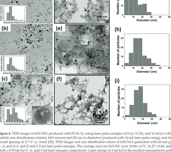
In the first study, InN-NCs were produced in ethanol with nanosecond PLAL of HPCVD-grown InN thin film on GaN/sapphire template substrate with different pulse energies [50]. Spherical InN-NCs within size ranges of 5.9–25.3, 5.4–34.8, and 3.24–36 nm were successfully produced using laser pulse energy values of 8, 12, and 16 mJ. The average diameter of the pro-duced InN-NCs was 10 nm (Figure 6a–c). TEM, Raman spectroscopy and XPS analysis con-firmed the production of InN-NCs. The UV/Vis/NIR spectrum analysis indicated the strong absorption edge from NIR region to UV region, which makes InN-NCs suitable candidates for photonics, optoelectronics, and biological applications [49].
Figure 6. TEM images of InN-NCs produced with PLAL by using laser pulse energies of 8 (a), 12 (b), and 16 mJ (c) with
particle size distributions (insets), InN nanocrystal (20 nm in diameter) produced with 16-mJ laser pulse energy and its crystal spacing of 2.7 A° (c, inset) [50]. TEM images and size distribution values of InN-NCs generated with (d and g) 3-, (e and h) 4- and (f and i) 5-mJ laser pulse energies. The average sizes for InN-NC were 10.84 ± 0.71, 16.27 ± 0.68, and 16.06 ± 0.59 nm for 3-, 4-, and 5-mJ laser energies, respectively. Laser energy of 3 mJ led to the smallest nanoparticles and narrower size distribution [51].
In the second study, to obtain ultra-small InN-NCs (<5 nm in diameter), the starting material was determined as InN powder target rather than HPCVD-grown InN thin film. It was shown that lower laser energy and lower ablation duration led to smaller nanoparticles. When ablation time is increased and the smaller nanoparticles are produced, they tended to aggregate. Hexagonal InN-NCs smaller than 5 nm in diameter were successfully produced in ethanol (Figure 6d–f) [51]. As a result, it was determined that the starting material, either a bulk target or a suspension, affects the final nanoparticle size in PLAL. In the literature, it was previously demonstrated that the ablation of suspensions leads to smaller nanoparticle dimensions compared to the ablation of bulk target. The particles in the suspension were suggested to absorb all the laser energy since they encounter a number of pulses during the whole ablation process as a result of con-tinuous stirring. By contrast, in case of ablation of the bulk target, laser energy is absorbed only by a specific point on the target leading to larger nanoparticles. Moreover, the nanoparticle size at the end of the PLAL depends on the initial size of the suspended particles [52, 53].
We showed that pure InN-NCs can be successfully produced with PLAL method. Other nitrides in the same group might also be successfully produced with PLAL. Moreover, low decomposition temperatures might be overcome for this kind of material. Therefore, this tech-nique might be successfully applied for the production of nanoparticles from other nitrides in the same group. As an outlook, femtosecond laser ablation might be performed to overcome the low decomposition temperature disadvantage of InN material.
2.2.5. MoS2 nanoparticles
The different geometries of MoS2 nanocrystal generation have been demonstrated by PLAL method in different liquids [54]. 3D MoS2 nanocrystals are generated in water, and 2D MoS2 nanosheets are generated in methanol as shown in Figure 7a. The optical microscope images of the MoS2 nanosheets are represented in Figure 7b. XRD analysis shows that the MoS2 nanosheets have a hexagonal crystal structure. The E1 2g and A1 g phonon modes are
Figure 7. (a) Scheme of the different-shaped MoS2 nanocrystals in different liquids and (b) optical microscope image of
determined by the peaks at 380.33 and 405.79 cm−1, respectively, by Raman spectroscopy.
This behavior of the generated nanocrystals in different liquids is associated with the chem-ical properties of the liquid where the laser ablation occurs. The ab initio calculation is used to examine the reason for the formation of 2D MoS2 in methanol and 3D MoS2 nanocrystals in water which are represented to correlate with vacancy formation.
2.3. Other types of nanoparticles produced by PLAL
2.3.1. Generation of nanoparticles from biological samples
Silica is useful for many plants, and a number of plants such as grasses, rice, sugar beet, and horse-tail contain high levels of biogenic silica [55]. Especially, sugar beet is an important bio-genic silica source since the silica content of this plant is mostly found in bagasse, which is pro-duced in significant amounts as a by-product in agricultural industry. On the other hand, silica has a number of application fields, in particular in drugs, cosmetics, printer toners, varnishes and food preservatives [53, 54]. Moreover, silica NPs are used in biomedical and biotechno-logical fields [56]. Thus, an environmentally friendly process for the production of silica NPs is crucial. A number of chemical methods were described in the literature for silica nanopar-ticle production [57, 58]. However, these chemical methods have various disadvantages such as being energy intensive, expensive, need for high temperatures, strong acidities and high pressures [59]. PLAL might be suggested as a suitable silica nanoparticle production method due to its versatility and low cost. Moreover, PLAL allows the synthesis of nanoparticles in large quantities. Our group demonstrated the production of silica nanoparticles by using the sugar beet bagasse as the target in PLAL since it contains large amounts of silica inherently. At the same time, chemical silica nanoparticle production method was utilized for the comparison of the end products. The successful silica nanoparticle production by PLAL was demonstrated with several characterization methods such as SEM, TEM, and dynamic light scattering (DLS). Silica nanoparticles with an average size of 74 nm were obtained with PLAL while chemical method resulted in a size range of 531–825 nm (Figure 8). Besides, silica nanoparticles produced with the chemical method resulted in a decrease in the growth of model aquatic algae. On the other hand, silica nanoparticles produced with PLAL led to an increase in the growth of these organisms. Due to the purity of silica nanoparticles produced by PLAL, this method might also be accepted as an environmentally friendly process for the nanoparticle production [60].
2.3.2. Nanocomposite generation
Significantly high surface-to-volume ratio of electrospun nanofibers and nanoparticles incor-porated into these nanofibers attract substantial attention recently. Functional nanofibrous structures with unique physical, chemical, optical, and catalytical properties might be obtained with this incorporation and they are used in different applications such as biotechnology, sen-sors, photonics, optoelectronics, energy, and so on [61, 62]. Although there are two different ways to obtain polymeric nanofibers containing NPs [63, 64], both of these approaches include a number of optimized process for every single material and require the utilization of toxic-reducing agents, stabilizers, protecting agents or surfactants. Our group demonstrated the suc-cessful production of Au-NPs in PVP polymer solution with PLAL method and PVP/Au-NP
solution was further electrospun to obtain uniform nanofibers. Here, PLAL was a clean, chemi-cally safe, and less time-consuming method for functional nanofibers containing nanoparticles. It can be suggested that other NPs can also be produced by PLAL in various polymer solutions. Thus, functional nanofibrous composites for different applications can be further developed depending on the NP and the polymer type [65].
3. Applications
3.1. Thin film MoS2 nanocrystal-based ultraviolet photodetector
MoS2 NCs-based photodetectors work well in the 300–400-nm UV range while omitting the response at the visible range due to MoS2 NC absorption properties [66]. The UV range response of MoS2 NCs generated by PLAL photodetectors gives a rise in the field of photon-ics and optoelectronphoton-ics due to their structural and optical properties. The absorption of MoS2 NCs synthesized by PLAL and the photodetectors based on them are very similar and their photoresponsivity has a good agreement. MoS2 NC-based photodetectors could be more advantageous compared to silicon- and germanium-based photodetectors because of their low oxidation tendency [67–70].
3.2. A plasmonic-enhanced photodetector based on silicon nanocrystals obtained through laser ablation
A photodetector that works at visible range is fabricated and its electrical properties are enhanced by adding Ag-NCs layer which improves the plasmonic effects where Si-NCs are synthesized by PLAL method and Ag NCs are generated by atomic layer deposition (ALD)-annealing technique [71]. The SEM image of the Ag-NCs is represented in Figure 9a and the inset shows the size distribution of the Ag-NCs. In Figure 9b, the schematic representation
Figure 8. (a) The diagram demonstrating the chemical and PLAL procedures used to produce silica nanoparticles from
sugar beet bagasse. The silica nanoparticle size distribution, (b) for the chemically produced nanoparticles, and (c) PLAL [60].
of the fabricated photodetector is shown where the active films (Si-NC and Ag-NCs) are sandwiched between insulating Al2O3 films. The absorption graph of the Ag nano islands is at the visible range and shown in Figure 9c. The photo-generated currents are measured for both cases; first one is without the Ag-NC film, and the second case is with the Ag-NC film. In Figure 1d, the measure photo-generated current versus wavelength is represented. The visible response is enhanced by adding Ag-NC film due to its plasmonic effects. Si-NC-based photodetector is widely used for visible range and its electronic and optical proper-ties could be improved by Ag-NC film because of its unique plasmonic effects.
3.3. A near-infrared range photodetector based on indium nitride nanocrystals obtained through laser ablation
Plasmonic properties of nanomaterials enable the optical tuning of near-infrared range plasmonic devices and they are frequently studied by many areas such as nanophotonics and telecommunication [72]. The large portion of solar spectrum consists of NIR range and this increases the importance of plasmonic-enhanced devices that work at this range [73]. Indium nitride nanocrystals (InN-NCs) have a NIR plasmonic resonance property [74, 75]. They also have a low band-gap energy, which is in the range of 0.7–0.9 eV, and they have unique electronic features such as high electron mobility, which allows fabricating high speed and high frequency electronic devices [76]. A near-infrared ranged photodetector has been demonstrated by using InN-NCs [77]. InN-NCs are generated by PLAL method from
Figure 9. (a) SEM image of Ag-NCs; inset: size distribution of them, (b) schematic representation of the photodetector, (c)
chemical vapor-deposited thin film. When 1-V bias is applied to the device, 600–1100-nm wavelength range photosensitivity is recorded. In Figure 10a, TEM images of InN-NCs syn-thesized by PLAL method are represented. In Figure 10b, 3D scheme of photodetector is shown, and in Figure 10c, the photoresponsivity versus wavelength graph is shown.
3.4. Enhancement in c-Si solar cells using 16-nm InN nanoparticles
To increase the performance of Si solar cells, InN-NCs are used. Higher performance depends on the low reflection that causes light scattering which allows enhancement between 400 and 620 nm [78]. This study was related with improving the anti-reflective coating (ARC) layers such as texturing for light trapping and layer designing [79–83]. Due to InN-NC coating, 9.67 and 16.42% improvements are obtained for short circuit current density and efficiency, respectively.
Figure 10. (a) TEM image of InN-NCs, (b) schematic of photodetector, and (c) photosensitivity versus wavelength graph
3.5. Enhanced memory effect via quantum confinement in 16-nm InN nanoparticles embedded in ZnO charge-trapping layer
The fabrication of charge-trapping memory cells with InN-NCs synthesized by PLAL method has been demonstrated with ZnO charge-trapping layer [84]. The observed memory hysteresis is very low without the InN-NCs. After InN-NCs enhancement, a 5-V memory window is achieved.
Figure 11. TEM images demonstrate the Ag-NP distribution in isolated rat hippocampal slice incubated with Ag-NPs, (a)
control; (b) and (c) Ag-NPs in the extracellular region; (d) Ag-NPs in the intracellular region, localized in the cytoplasm; (e) phagocytosis of Ag-NPs. Arrows show the Ag-NPs. Scale bar for each figure is 500 nm [21].
3.6. Biological applications
Pure uncoated Ag-NPs were used for the evaluation of Ag-NP toxicity in an aquatic mac-rophyte and in rat hippocampus cells. It was shown that Ag-NPs led to a dose-dependent toxicity in lower nanoparticle concentrations, which implies that accidental contamination of water sources with Ag-NP at low doses might result in significant ecological toxicity [19]. In the other toxicity study, the purity of Ag-NPs produced by PLAL method led to the understanding of the importance of surface chemistry and the size for the uptake mecha-nism of Ag-NPs into isolated rat hippocampal cells. It was demonstrated that phagocytosis was endocytotic pathway type for the entry of larger Ag-NPs into the hippocampal neurons (Figure 11) [21].
4. Conclusion
Nanoparticle production is a crucial part of the nanoscience which leads to several applica-tions in physics, electronics, medicine, biology and industry. As the scale goes down to nano, materials exhibit unique properties compared to their macroscale bulk counterparts. To reveal such properties, reaching nanoscale material production has become an issue. PLAL is a fast and cheap method to obtain pure nanomaterials in organic solutions. Also, it is easy to apply to different materials since it does not require high temperature and high-pressure conditions. The presented results demonstrate both nanomaterial generations and their applications are successfully achieved with various materials. To sum up, PLAL is a powerful nanomaterial generation method that is already demonstrated with different types of materials and appli-cations successfully. Additionally, PLAL is a promising technique to become mass nanomate-rial production with its unique properties.
Acknowledgements
The authors thank the Turkish Academy of Science—Outstanding Young Scientist Award Program (TUBA-GEBIP).
Author details
Bülend Ortaç*, Elif Uzcengiz Şimşek and Canan Kurşungöz *Address all correspondence to: [email protected]
National Nanotechnology Research Center (UNAM), Institute of Materials Science and Nanotechnology, Bilkent University, Ankara, Turkey
References
[1] Oberdörster G, Oberdörster E, Oberdörster J. Review nanotoxicology: An emerging dis-cipline evolving from studies of ultrafine particles. Environmental Health Perspectives. 2005;113(7):823-839
[2] Baeuerle D. Laser Processing and Chemistry. Linz, Austria: Springer Science & Business Media; 2000
[3] Ghofraniha N, Conti C, Ruocco G, Trillo S. Shocks in nonlocal media. Physical Review Letters. 2007;99(4):43903
[4] Staudt W, Borneis S, Pippert K-D. TFT annealing with excimer laser. Technology and market outlook. Physica Status Solidi. 1998;166(2):743-749
[5] Chrisey, Douglas B, Hubler GK. Pulsed Laser Deposition of Thin Films. New York: Wiley; 1994. p. 55
[6] Voloshko A, Itina TE. Nanoparticle formation by laser ablation and by spark discharges-properties, mechanisms, and control possibilities. In: Nanoparticles Technology. InTech; 2015
[7] Xu X, Duan G, Li Y, Liu G, Wang J, Zhang H, Dai Z, Cai W. Fabrication of gold nanopar-ticles by laser ablation in liquid and their application for simultaneous electrochemical detection of Cd2+, Pb2+, Cu2+, Hg2+. ACS Applied Materials & Interfaces. 2013;6(1):65-71 [8] Correard F, Maximova K, Estève MA, Villard C, Roy M, Al-Kattan A, Sentis M, Gingras
M, Kabashin AV, Braguer D. Gold nanoparticles prepared by laser ablation in aqueous biocompatible solutions: Assessment of safety and biological identity for nanomedicine applications. International Journal of Nanomedicine. 2014;9:5415
[9] Burzhuev S, Dâna A, Ortac B. Laser synthesized gold nanoparticles for high sensitive strain gauges. Sensors and Actuators A: Physical. 2013;203:131-136
[10] Zamborini FP, Leopold MC, Hicks JF, Kulesza PJ, Malik MA, Murray RW, et al. Electron hopping conductivity and vapor sensing properties of flexible network polymer films of metal nanoparticles. Journal of the American Chemical Society. 2002;124(30):8958-8964 [11] Herrmann J, Müller KH, Reda T, Baxter GR, Raguse BD, De Groot GJJB, Chai R, Roberts
M, Wieczorek L. Nanoparticle films as sensitive strain gauges. Applied Physics Letters. 2007;91(18):183105
[12] Wiesner MR, Lowry GV, Alvarez P, Dionysiou D, Biswas P. Assessing the risks of manu-factured nanomaterials. Environmental Science & Technology. 2006;4336-4345
[13] Navarro E, Piccapietra F, Wagner B, Marconi F, Kaegi R, Odzak N, et al. Toxicity of silver nanoparticles to Chlamydomonas reinhardtii. Environmental Science & Technology. 2008;42(23):8959-8964
[14] Chen X, Schluesener HJ. Nanosilver: A nanoproduct in medical application. Toxicology Letters. 2008;176(1):1-12
[15] Evanoff DD, Chumanov G. Synthesis and optical properties of silver nanoparticles and arrays. ChemPhysChem. 2005;6(7):1221-1231
[16] Pingali KC, Rockstraw DA, Deng S, Pingali KC, Rockstraw DA, Deng S. Aerosol science and technology silver nanoparticles from ultrasonic spray pyrolysis of aqueous silver nitrate. Aerosol Science and Technology. 2005;39(10):1010-1014
[17] Barcikowski S, Hahn A, Walter J. Health risks of nanoparticulate emissions during fem-tosecond and picosecond pulsed laser machining. In: Proc SPIE 7201, Laser Applications in Microelectronic and Optoelectronic Manufacturing VII. 2009. p. 720109
[18] Akman E, Oztoprak BG, Gunes M, Kacar E, Demir A. Effect of femtosecond Ti : Sapphire laser wavelengths on plasmonic behaviour and size evolution of silver nanoparticles. Photonics and Nanostructures-Fundamentals and Applications. 2011;9(3):276-286
[19] Üçüncü E, Özkan AD, Kurşungöz C, Ülger ZE, Ölmez TT, Tekinay T, et al. Effects of laser ablated silver nanoparticles on Lemna minor. Chemosphere. 2014;108:251-257
[20] Bruchez M, Moronne M, Gin P, Weiss S, Alivisatos AP. Semiconductor nanocrystals as fluorescent biological labels. Science (80- ). 1998;281(5385):2013-2016
[21] Kursungoz C, Taş ST, Sargon MF, Sara Y, Ortaç B. Toxicity of internalized laser gen-erated pure silver nanoparticles to the isolated rat hippocampus cells. Toxicology & Industrial Health. 2017;1-9
[22] Torchynska TV, Vasilievitch YV. Nanocrystals and Quantum Dots of Group IV Semiconductors. American Scientific Publ.; 2010
[23] Trindade T, Brien PO, Pickett NL. Nanocrystalline semiconductors: synthesis, proper-ties, and perspectives. Chemistry of Materials. 2001;13(11):3843-3858
[24] Hu MS, Wang WM, Chen TT, Hong LS, Chen CW, Chen CC, et al. Sharp infrared emis-sion from single-crystalline indium nitride nanobelts prepared using guided-stream thermal chemical vapor deposition. Advanced Functional Materials. 2006;16(4):537-541 [25] Lambert TN, Andrews NL, Gerung H, Boyle TJ, Oliver JM, Wilson BS, et al.
Water-soluble germanium(0) nanocrystals: Cell recognition and near-infrared photothermal conversion properties. Small. 2007;3(4):691-699
[26] Prabakar S, Shiohara A, Hanada S, Fujioka K, Yamamoto K, Tilley RD. Size controlled synthesis of germanium nanocrystals by hydride reducing agents and their biological applications. Chemistry of Materials. 2009;22(2):482-486
[27] Cheng K, Anthony R, Kortshagen UR, Holmes RJ. High-efficiency silicon nanocrystal light-emitting devices. Nano Letters. 2011
[28] Henderson EJ, Seino M, Puzzo DP, Ozin GA. Colloidally stable germanium nanocrystals for photonic applications. ACS Nano. 2010;4(12):7683-7691
[29] Danek M, Jensen KF, Murray CB, Bawendi MG. Synthesis of luminescent thin-film CdSe/ ZnSe quantum dot composites using CdSe quantum dots passivated with an overlayer of ZnSe. Chemistry of Materials. 1996;8(3):173-180
[30] Holman ZC, Liu CY, Kortshagen UR. Germanium and silicon nanocrystal thin-film field-effect transistors from solution. Nano Letters. 2010;10(7):2661-2666
[31] Guo Z, Zhang D, Wei S, Wang Z, Karki AB, Li Y, et al. Effects of iron oxide nanoparticles on polyvinyl alcohol: Interfacial layer and bulk nanocomposites thin film. Journal of Nanoparticle Research. 2010;12(7):2415-2426
[32] Wender H, Andreazza ML, Correia RRB, Teixeira SR, Dupont J, Schmid G, et al. Synthesis of gold nanoparticles by laser ablation of an Au foil inside and outside ionic liquids. Nanoscale. 2011;3(3):1240
[33] Ortaç B, Kayaci F, Vural HA, Deniz AE, Uyar T. Photoluminescent electrospun polymeric nanofibers incorporating germanium nanocrystals. Reactive and Functional Polymers. 2013;73(9):1262-1267
[34] Švrček V, Sasaki T, Shimizu Y, Koshizaki N. Blue luminescent silicon nanocrystals pre-pared by ns pulsed laser ablation in water. Applied Physics Letters. 2006;89(21)
[35] Yang S, Cai W, Zeng H, Li Z. Polycrystalline Si nanoparticles and their strong aging enhancement of blue photoluminescence. Journal of Applied Physics. 2008;104(2)
[36] Abderrafi K, Raul GC, Gongalsky MB, Suarez I, Abarques R, Chirvony VS, et al. Silicon nanocrystals produced by nanosecond laser ablation in an organic liquid. Journal of Physical Chemistry C. 2011;115:5147-5151
[37] Alkis S, Okyay AK, Ortaç B. Post-treatment of silicon nanocrystals produced by ultra-short pulsed laser ablation in liquid: Toward blue luminescent nanocrystal generation. Journal of Physical Chemistry C. 2012;116(5):3432-3436
[38] Akasaki I, Amano H. Crystal growth and conductivity control of group III nitride appli-cation to short wavelength light emitters semiconductors and their. Japanese Journal of Applied Physics. 1997;36(9R):5393
[39] Kazlauskas K, Tamulaitis G, Žukauskas A, Khan MA, Yang JW, Zhang J, et al. Exciton and carrier motion in quaternary AllnGaN. Applied Physics Letters. 2003;82(25):4501-4503 [40] Son KA, Liao A, Lung G, Gallegos M, Hatake T, Harris RD, Scheick LZ, Smythe W.
GaN-based high temperature and radiation-hard electronics for harsh environments. Nanoscience and Nanotechnology Letters. 2010;2(2):89-95
[41] Borsella E, Garcia MA, Mattei G, Maurizio C, Mazzoldi P, Cattaruzza E, et al. Synthesis of GaN quantum dots by ion implantation in dielectrics. Journal of Applied Physics. 2001;90(9):4467-4473
[42] Miyamura M, Tachibana K, Arakawa Y. High-density and size-controlled GaN self-assembled quantum dots grown by metalorganic chemical vapor deposition. Applied Physics Letters. 2002;80(21):3937-3939
[43] Gyger F, Bockstaller P, Gröger H, Gerthsen D, Feldmann C. Quantum-confined GaN nanoparticles synthesized via liquid-ammonia-in-oil-microemulsions. Chemical Comm-u nications. 2014;50(22):2939
[44] Petersen S, Barcikowski S. In situ bioconjugation: Single step approach to tailored nanoparticle-bioconjugates by ultrashort pulsed laser ablation. Advanced Functional Materials. 2009;19(8):1167-1172
[45] Wu H, Yang R, Song B, Han Q, Li J, Zhang Y, et al. Biocompatible inorganic fullerene-like molybdenum disulfide nanoparticles produced by pulsed laser ablation in water. ACS Nano. 2011;5(2):1276-1281
[46] Demirel A, Öztaş T, Kurşungöz C, Yılmaz İ, Ortaç B. Synthesis of blue-shifted lumines-cent colloidal GaN nanocrystals through femtosecond pulsed laser ablation in organic solution. Journal of Nanoparticle Research. 2016;18(5):1-10
[47] Mohammad S, Noor HM. Progress and prospects of group-III nitride semiconductors. Progress in Quantum Electronics. 1996;20(5-6):361-525
[48] Wu C, Li T, Lei L, Hu S, Liu Y, Xie Y, et al. Indium nitride from indium iodide at low temperatures: Synthesis and their optical properties. New Journal of Chemistry. 2005;29:1610-1615
[49] Chen Z, Li Y, Cao C, Zhao S, Fathololoumi S, Mi Z, et al. Large-scale cubic InN nanocrys-tals by a combined solution- and vapor-phase method under silica confinement. Journal of the American Chemical Society. 2012;134(2):780-783
[50] Alkis S, Alevli M, Burzhuev S, Vural HA, Okyay AK, Ortaç B. Generation of InN nano-crystals in organic solution through laser ablation of high pressure chemical vapor depo-sition-grown InN thin film. Journal of Nanoparticle Research. 2012;14(8)
[51] Kurşungöz C, Şimşek EU, Tuzaklı R, Ortaç B. Generation of ultra-small InN nano-crystals by pulsed laser ablation of suspension in organic solution. Applied Physics A. 2017;123(3):209
[52] Kim D, Jang D. Synthesis of nanoparticles and suspensions by pulsed laser ablation of microparticles in liquid. Applied Surface Science. 2007;253(19):8045-8049
[53] Zeng H, Du XW, Singh SC, Kulinich SA, Yang S, He J, et al. Nanomaterials via laser abla-tion/irradiation in liquid: A review. Advanced Functional Materials. 2012;22(7):1333-1353 [54] Oztas T, Sen HS, Durgun E, Ortaç B. Synthesis of colloidal 2D/3D MoS2 nanostructures
by pulsed laser ablation in organic liquid environment. Journal of Physical Chemistry C. 2014;118:30120
[55] Sun L, Carbide S, Sic P. Silicon-based materials from rice husks and their applications. Industrial & Engineering Chemistry Research. 2001;40(25):5861-5877
[56] Clément L, Zenerino A, Hurel C, Amigoni S, Taffin de Givenchy E, Guittard F, et al. Toxicity assessment of silica nanoparticles, functionalised silica nanoparticles, and HASE-grafted silica nanoparticles. Science of the Total Environment. 2013;450-451:120-128 [57] Cadby AJ, Tolbert SH. Controlling optical properties and interchain interactions in
semi-conducting polymers by encapsulation in periodic nanoporous silicas with different pore sizes. Journal of Physical Chemistry B. 2005;109(38):17879-17886
[58] Molenkamp WC, Watanabe M, Miyata H, Tolbert SH. Highly polarized luminescence from optical quality films of a semiconducting polymer aligned within oriented meso-porous silica. Journal of the American Chemical Society. 2004;126(14):4476-4477
[59] Bansal V, Ahmad A, Sastry M. Fungus-mediated biotransformation of amorphous silica in rice husk to nanocrystalline silica. Journal of the American Chemical Society. 2006;128(43):14059-14066
[60] San NO, Kurşungöz C, Tümtaş Y, Yaşa Ö, Ortaç B, Tekinay T. Novel one-step synthesis of silica nanoparticles from sugarbeet bagasse by laser ablation and their effects on the growth of freshwater algae culture. Particuology. 2014;17:29-35
[61] Ramakrishna S, Fujihara K, Teo WE, Yong T, Ma Z, Ramaseshan R. Electrospun nanofi-bers: Solving global issues. Mater Today. 2006;9(3):40-50
[62] Teo WE, Ramakrishna S. Electrospun nanofibers as a platform for multifunctional, hierarchically organized nanocomposite. Vol. 69, Composites Science and Technology. Elsevier Ltd; 2009. pp. 1804-1817
[63] Wang Y, Yang Q, Shan G, Wang C, Du J, Wang S, et al. Preparation of silver nanoparticles dispersed in polyacrylonitrile nanofiber film spun by electrospinning. Materials Letters. 2005;59(24-25):3046-3049
[64] He D, Hu B, Yao QF, Wang K, Yu SH. Large-scale synthesis of flexible free-standing SERS substrates with high sensitivity: electrospun PVA nanofibers embedded with con-trolled alignment of silver nanoparticles. ACS Nano. 2009;3(12):3993-4002
[65] Deniz AE, Vural HA, Ortaç B, Uyar T. Gold nanoparticle/polymer nanofibrous com-posites by laser ablation and electrospinning. Materials Letters. 2011;65(19-20):2941-2943 [66] Alkis S, Öztaş T, Aygün LE, Bozkurt F, Okyay AK, Ortaç B. Thin film MoS2 nanocrystal
based ultraviolet photodetector. Optics Express. 2012;20(19):21815-21820
[67] Li Q, Newberg JT, Walter EC, Hemminger JC, Penner RM. Polycrystalline molybdenum disulfide (2H-MoS2) nano-and microribbons by electrochemical/chemical synthesis. Nano Letters. 2004;4(2):277-281
[68] Shanmugam M, Bansal T, Durcan CA, Yu B. Molybdenum disulphide/titanium dioxide nanocomposite-poly 3-hexylthiophene bulk heterojunction solar cell. Applied Physics Letters. 2012;100(15):153901
[69] Yoon Y, Ganapathi K, Salahuddin S. How good can monolayer MoS2 transistors be? Nano Letters. 2011;11(9):3768-3773
[70] Ross S, Sussman A. Surface oxidation of molybdenum disulfide. Journal of Physical Chemistry. 1955;59(9):889-892
[71] Alkis S, Oruç FB, Ortaç B, Koşger AC, Okyay AK. A plasmonic enhanced photodetec-tor based on silicon nanocrystals obtained through laser ablation. Journal of Optics. 2012;14(12):125001
[72] Palomaki PKB, Miller EM, Neale NR. Control of plasmonic and interband transitions in colloidal indium nitride nanocrystals. Journal of the American Chemical Society. 2013;135(38):14142-14150
[73] Paz-Soldan D, Lee A, Thon SM, Adachi MM, Dong H, Maraghechi P, et al. Jointly tuned plasmonic-excitonic photovoltaics using nanoshells. Nano Letters. 2013;13(4):1502-1508 [74] Sardar K, Deepak FL, Govindaraj A, Seikh MM, Rao CNR. InN nanocrystals, nanowires,
and nanotubes. Small. 2005;1(1):91-94
[75] Hsieh JC, Yun DS, Belcher AM. Ambient pressure, low-temperature synthesis and characterization of colloidal InN nanocrystals. Journal of Materials Chemistry. 2010;
20(8):1435-1437
[76] Mohammad SN, Morkoç H. Progress and prospects of group-III nitride semiconductors. Progress in Quantum Electronics. 1996;20(5-6):361-525
[77] Tekcan B, Alkis S, Alevli M, Dietz N, Ortac B, Biyikli N, et al. A near-infrared range pho-todetector based on indium nitride nanocrystals obtained through laser ablation. IEEE Electron Device Letters. 2014;35(9):936-938
[78] Chowdhury FI, Alnuaimi A, Alkis S, Ortaç B, Aktürk S, Alevli M, et al. Enhancement in c-Si solar cells using 16nm InN nanoparticles. Materials Research Express. 2016;56202 [79] Wang Y, Zhang X, Bai L, Huang Q WZY. Effective light trapping in thin film silicon solar
cells from textured Al doped ZnO substrates with broad surface feature distributions. Applied Physics Letters. 2012;263508
[80] Tark SJ, Kang MG, Park S, Jang JH, Lee JC, Kim WM, Lee JS, Kim D. Development of surface-textured hydrogenated ZnO:Al thin-films for μc-Si solar cells. Current Applied Physics. 2009;9:1318-1322
[81] Anna Selvan JA, Delahoy AE, Guo S, Li Y-M. A new light trapping TCO for nc-Si:H solar cells. Solar Energy Materials and Solar Cells. 2006;90:3371-3376
[82] Meiners B-M, Holinski S, Schäfer P, Hohage S, Borchert D. Investigation of anti-reflection coating stacks for silicon heterojunction solar cells. In: 29th European PV Solar Energy Conf and Exhibition. 2014
[83] Chowdhury FI, Blaine T, Gougam AB. Optical transmission enhancement of fluorine doped tin oxide (FTO) on glass for thin film photovoltaic applications. Energy Procedia. 2013;42:660-669
[84] Nazek El-Atab AN, Cimen F, Alkis S, Ortaç B, Alevli M, Dietz N, Okyay AK. Enhanced memory effect via quantum confinement in 16 nm InN nanoparticles embedded in ZnO charge trapping layer. Applied Physics Letters. 2014;104:253106
![Figure 3. SEM images of (a) PVA nanofibers, (b) Ge-NCs/PVA nanofibers (the insets represent the high magnification SEM images), (c) STEM image of Ge-NCs/PVA nanofiber [33], (d) EDX data of Ge-NCs/PVA.](https://thumb-eu.123doks.com/thumbv2/9libnet/5897244.121972/7.918.136.787.236.1193/figure-images-nanofibers-nanofibers-insets-represent-magnification-nanofiber.webp)