Confined states in multiple quantum well structures of Si
nGe
nnanowire superlattices
N. Akman,1 E. Durgun,2,3S. Cahangirov,3 and S. Ciraci2,3,
*
1Department of Physics, Mersin University, Mersin 33343, Turkey 2Department of Physics, Bilkent University, Ankara 06800, Turkey3UNAM-Institute for Materials Science and Nanotechnology, Bilkent University, Ankara 06800, Turkey 共Received 7 September 2007; published 21 December 2007兲
Mechanical properties, atomic and energy band structures of bare and hydrogen-passivated SinGennanowire superlattices have been investigated by using first-principles pseudopotential plane-wave method. Undoped, tetrahedral Si and Ge nanowire segments join pseudomorphically and can form superlattice with atomically sharp interface. We found that Sinnanowires are stiffer than Gennanowires. Hydrogen passivation makes these
nanowires and SinGen nanowire superlattice even more stiff. Upon heterostructure formation, superlattice
electronic states form subbands in momentum space. Band lineups of Si and Ge zones result in multiple quantum wells, where specific states at the band edges and in band continua are confined. The electronic structure of the nanowire superlattice depends on the length and cross section geometry of constituent Si and Ge segments. Since bare Si and Ge nanowires are metallic and the band gaps of hydrogenated ones vary with the diameter, SinGensuperlattices offer numerous alternatives for multiple quantum well devices with their
leads made from the constituent metallic nanowires.
DOI:10.1103/PhysRevB.76.245427 PACS number共s兲: 61.46.⫺w, 68.65.Cd, 73.20.At, 73.21.Fg
I. INTRODUCTION
Planar superlattices have been fabricated either through periodic junction of alternating semiconductor layers with different band gaps or through repeating compositional modulation. Electrons in parallel layers show two-dimensional共2D兲 free electronlike behavior and have quan-tization different from those three-dimensional bulk semi-conductors. Minibands in the momentum space in the direction perpendicular to the layers and periodically varying band gap in the direct space have attributed unusual elec-tronic functions for novel devices. These devices are field effect transistors, photodetectors, light emitting diodes 共LEDs兲, quantum cascade lasers, etc.
Recently, new growth techniques have enabled also the synthesis of one-dimensional 共1D兲 nanowire superlattices 共NWSLs兲. NWSLs from groups III–V and group IV elements have been synthesized successfully. InAs/InP superlattices1
with atomically perfect interfaces and with periods of several nanometers could be realized using techniques, such as mo-lecular beam epitaxy and nanocluster catalyst. Furthermore, compositionally modulated superlattices of GaAs/GaP have been synthesized by laser-assisted catalytic growth technique,2again with atomically perfect interfaces and with
the component layers ranging from 2 to 21. It is proposed that these NWSLs can offer potential applications in nano-electronics such as optical nanobar codes, 1D waveguides, and polarized nanoscale LEDs. Longitudinal Si/Si-Ge NWSLs with nanowire diameter ranging from 50 to 300 nm have also been synthesized using laser ablation growth technique.3Structural parameters such as nanowire diameter,
Ge concentration, and the modulation period in the Si/Si-Ge superlattices can be controlled easily by adjusting the reac-tion condireac-tions. Technological applicareac-tions such as LEDs and thermoelectric devices have been suggested. In addition to the longitudinal 共axial兲 nanowire superlattices, coaxial core-shell and core-multishell nanowire heterostructures
have attracted interest recently. Crystalline Si/Ge and Ge/Si core-shell structures have been experimentally synthesized by Lauhon et al.4Most of works involved in 1D superlattices
especially concern the experimental synthesis and character-ization of coaxial nanowire heterostructures.
Theoretically, only a few works investigated core-shell and longitudinal NWSLs.5–8Kagimura et al.6reported an ab initio study of the electronic properties of Si and Ge nano-wires and Si/Ge heterostructures with one surface dangling bond state per unit cell. They concluded that surface dan-gling bond level observed in the band gap of nanowires and nanowire heterostructures can be used as reference level to estimate band lineups in these systems. Using one-band ef-fective mass theory, a criterion has been developed for the occurrence of longitudinal barrier height.7It has been argued
that radial confinement reduces the actual barrier height in modulated nanowire superlattices. Zypman8 used the
Hub-bard model to get the energy spectrum of one-dimensional systems and applied their results to various model systems such as nanowire tunneling diodes and Si/Ge superlattice nanowires to interpret the scanning tunneling spectroscopy measurements. Earlier formation of multiple quantum well structure and resulting confined states on hydrogenated or radially deformed carbon nanotubes have also been reported.9
In this paper, we have investigated the mechanical prop-erties and atomic and electronic structures of bare and hy-drogenated SinGen nanowire superlattices using first-principles plane-wave method. NWSLs are constructed from alternating Si and Ge nanowire segments共zones兲, both have same orientation and similar atomic structure. These seg-ments are joined pseudomorphically and formed a sharp in-terface. We found that even small diameter hydrogenated SinGenNWSLs form multiple quantum well structures where conduction and valence band electrons are confined. Our study indicates that the band lineup and resulting electronic structure depend on the length and cross section geometry of the constituent Sin and Gennanowires.
II. METHOD
We have performed first-principles plane-wave calculations10,11 within density functional theory 共DFT兲12 using ultrasoft pseudopotentials.11,13 The exchange
correla-tion potential has been approximated by generalized gradient approximation 共GGA兲 using PW91 functional.14 For partial
occupancies, we use the Methfessel-Paxton smearing method.15 The adopted smearing width is 0.1 eV for the atomic relaxation and 0.02 for the accurate band structure analysis and density of state calculations. All structures have been treated within a supercell geometry using the periodic boundary conditions. The lattice parameters of the tetragonal supercell are asc, bsc, and csc. We took asc= bsc= 27 Å for NWSL having the largest diameter共⬃1.8 nm兲, but asc= bsc = 22 Å for one having the smallest diameter共⬃1.2 nm兲 con-sidered in this paper. These values allowed minimum dis-tance ranging from⬃11 to 14 Å between two atoms in dif-ferent adjacent cells, so that their coupling is hindered significantly. We took cscequal to the lattice constant c of the nanowires and NWSLs under consideration. In the self-consistent potential and total energy calculations the Bril-louin zone 共BZ兲 is sampled in the k space within the Monkhorst-Pack scheme16 by 共1⫻1⫻9兲 mesh points for single unit cell and, for example,共1⫻1⫻5兲 mesh points for double cells. A plane-wave basis set with kinetic energy of up to 250 eV has been used. All atomic positions and lattice constant csc= c are optimized by using the conjugate gradient method where total energy and atomic forces are minimized. The criterion of convergence for energy is chosen to be 10−5eV between two ionic steps, and the maximum force allowed on each atom is 0.05 eV/Å.
III. BARE AND HYDROGENATED NANOWIRES AND NANOWIRE SUPERLATTICES
In this study, we considered bare and hydrogen-passivated longitudinal SinGennanowire superlattices and also bare and hydrogen-passivated Si and Ge nanowires as constituent structures. Bare Si and Ge nanowires are oriented along the 关001兴 direction of the parent diamond crystal and have nor-mally N atoms in their primitive unit cell with lattice con-stant c along the nanowire 共or z兲 axis. We took N=25 and N = 57 as two special prototypes. We designate them as SiNW共n兲 关GeNW共n兲兴 or shortly Sin共Gen兲 with n=sN, s be-ing an integer number. Sin and SiN 共Gen and GeN兲 indicates the same nanowire, except that the unit cell of the former one includes s primitive cell in direct space with 1/s times re-duced BZ in the momentum space. In our simulations, bare Sin 共Gen兲 nanowires are first cut from the bulk crystal with ideal structural parameters. Subsequently, ideal bare nano-wires are relaxed to optimize their structure and lattice con-stant. Si共Ge兲 atoms near the core of relaxed nanowire have tetrahedral coordination. To obtain H-passivated Sin or Gen nanowires 共designated as H-SiNW共n兲 or H-GeNW共n兲, shortly as H-Sinor H-Gen兲, the dangling bonds at the surface are saturated by H atoms and whole structure is reoptimized. Our study indicates that the atomic and electronic structure of H-Sin and H-Gen may depend on whether hydrogen
pas-sivation and subsequent optimization are achieved on ideal or optimized bare Sin and Gen nanowires. The present se-quence of structure optimization mimics the actual growth of hydrogen-passivated nanowires.
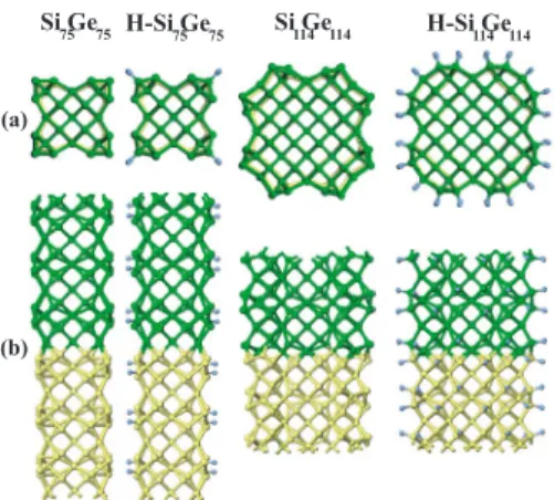
A SinGen has n = sN Si atoms at one side and n = sN Ge atoms at the other side of NWSL unit cell. These atoms have tetrahedral coordination as if they are part of a SiGe hetero-structure, and hence at the interface, Si atoms are bonded to Ge atoms pseudomorphically and make atomically flat inter-face. We note that pseudomorphic growth can sustain for small diameters; but misfit dislocations may be generated at the interface of large diameter共or large N兲 SinGen superlat-tice. Atomic positions and lattice constant are relaxed to ob-tain optimized structure. H-SinGenfollow the same sequence of construction as H-Sin or H-Gen. Optimized lattice con-stants of bare SinGennanowire superlattice for n = 25, 50, and 75 are found to have c = 10.9, 21.8, and 32.7 Å, respectively. Upon hydrogenation, these lattice constants change to c = 11.2, 22.3, and 33.5 Å, respectively. Lattice constants of bare and hydrogenated SinGen, n = 57 and 114, are almost identical and are c = 11.1 and 22.2 Å, respectively. Figure1
shows the atomic structure of bare and hydrogen-passivated SinGenfor n = 75 and 114. These NWSLs are reminiscent of SinGen 共001兲 planar superlattice, which were fabricated by molecular beam epitaxy by growing first the n Si共001兲 plane and then n Ge共001兲 plane and eventually by repeating this SinGen共001兲 unit periodically. While the SinGen共001兲 super-lattice has 2D periodicity in the共001兲 layers, NWSLs under study here have finite cross section and hence 2D periodicity is absent. Electrons are bound to NWSL in radial 共lateral兲 direction but propagate as 1D Bloch states along the super-lattice axis共in longitudinal direction兲.
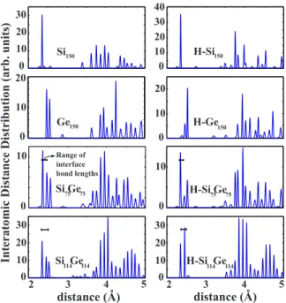
Interatomic distance distributions of Si75Ge75 and
H-Si75Ge75 NWSLs are compared with parent Si and Ge
nanowires in Fig. 2. In the same figure, we also show the interatomic distance distribution of bare and hydrogenated Si114Ge114 NWSL. At the surface, optimized atomic struc-tures of Sin and Gen deviate considerably from the ideal structure of Sinand Gen. For example, one can deduce
quad-Si Ge75 75 H-Si Ge75 75 Si Ge114 114 H-Si Ge114 114
(a)
(b)
FIG. 1. 共Color online兲 Optimized atomic structure of bare and hydrogenated SinGennanowire superlattices for n = 75 and 114.共a兲
Top view and共b兲 side view. Small-gray, large-light, and large-dark balls correspond to the hydrogen, silicon, and germanium atoms, respectively.
rangles of atoms at the surface. Normally, NWSLs consist of hexagonal and pentagonal rings, where one can distinguish bond lengths in different categories. The interatomic distance distribution of SinGen is reminiscent of the sum of those of Si2n and Ge2n except some changes originated from the
in-terface between Si and Ge segments of supercell. While bulk optimized Si-Si and Ge-Ge bond lengths are d = 2.36, and 2.50 Å, respectively, the Si-Ge bond at the interface ranges between 2.35 and 2.52 Å for bare Si228Ge228共between 2.37
and 2.49 Å for H-Si228Ge228兲. Nevertheless, the distribution
exhibits several peaks corresponding to the deviations from the bulk geometry at the surface. As the cross section or N increases, the effect of the surface decreases and the distri-bution of interatomic distances becomes more bulklike.
IV. MECHANICAL PROPERTIES
The stability and elastomechanical properties of SinGen and H-SinGen NWSLs are crucial for their possible use in nanoelectronics. In the present study, the maximum diameter of nanowire we treated is⬃1.8 nm. The diameter of hydro-genated Si25Ge25 NWSL is even smaller 共⬃1.4 nm兲. For such small diameter nanowires or NWSLs, there are ambi-guities in determining the area of cross section. Moreover, the surface to volume ratio is rather high and hence makes the cross section nonuniform. In view of these, the calcula-tion of Young’s modulus may not be appropriate. Here, we rather considered the force 共spring兲 constants of nanowires and NWSLs under a strain in the harmonic region. To this end, we calculated the second derivative of the total energy 共per unit cell兲 with respect to the lattice constant c 共i.e., = d2E
T/dc2兲 or to the strain, ⑀=⌬c/c 共i.e., ⬘= d2ET/d⑀2兲.
The values calculated for nanowires and NWSLs treated in our paper are given in TableI.
Like bulk crystals, Sin nanowires are stiffer than Gen nanowires. This implies that the lattice mismatch between Si and Ge nanowires in NWSL is accommodated mainly by the Ge zone. For both nanowires and NWSL, increases with increasing cross section. For example,of Si25is almost the half of of Si57. Note that 共Si50兲⯝共Si25兲/2. As for of
Si25Ge25 NWSL calculated from first principles is
2.18 eV/Å. This value can be estimated in terms of two springs connected in series, namely, −1共Si
25Ge25兲
⯝−1共Si
25兲+−1共Ge25兲 to be 共Si25Ge25兲⯝2.08 eV/Å. We,
therefore, conclude that as long as the geometry and size of the cross section remained to be similar, classical Hook’s law continues to be approximately valid even for nanostructures. Upon hydrogenation, both nanowires as well as NWSLs studied here become stiffer. The spring constant of Si57Ge57
is twice that of Si114Ge114because the latter NWSL has twice the length of the former. We also calculated18the ratio of the
strain of the Ge zone to that of Si zone of Si75Ge75 under
tensile stress, i.e., ⑀共Ge兲/⑀共Si兲 to be ⬃2.5. This ratio is re-duced to ⬃1.25 for Si114Ge114. In compliance with the
values in Table I, this result indicates that in a SinGen, NWSL Ge zone elongates more than Si zone. Using empiri-cal potential, Menon et al.17 were able to calculate the
Young’s modulus and bending stiffness of tetrahedral and cagelike Si nanowire of⬃4 nm diameter and found values comparable with bulk values.
10 20 30 0 0 10 20 0 10 Si Ge Interatomic Distance Distribution (arb. units) 10 20 30 40 10 20 0 10 0 distance (A) H-Si Ge75 75 75 75 0 distance (A) Ge150 Si150 H-Si150 H-Ge150 o o 10 0 20 30 Si Ge 10 20 30 H-Si Ge114 114 114 114 0 2 3 4 5 2 3 4 5 Range of interface bond lengths
FIG. 2.共Color online兲 Interatomic distance distribution of opti-mized bare and hydrogenated Si2n, Ge2n, and SinGenfor n = 75 up to
fourth nearest neighbor. Similar distributions for Si114Ge114 and H-Si114Ge114are also shown. The Si-H共Ge-H兲 bond lengths being in the range of⬃1.5 Å are not shown.
TABLE I. Equilibrium values of lattice parameter c are given in units of Å. Force constant 共as defined in the text兲, in units of eV/Å, is calculated by using bothVASPresult and Hook’s law. Per-centage difference in between force constant values calculated from
VASPresult and Hook’s law is given within parenthesis in order to check whether classical Hook’s law is still valid in nanoscale. Also force constant⬘共as defined in the text兲 is presented in units of eV.
Structure c0 Hook’s law ⬘
Si25 5.32 5.68 161 Ge25 5.57 3.28 102 Si25Ge25 10.90 2.18 2.08 共5兲 259 Si50Ge50 21.75 0.92 1.04 共12兲 437 Si75Ge75 32.70 0.62 0.69 共10兲 663 Si57 5.43 11.22 327 Ge57 5.65 7.49 239 Si57Ge57 11.07 4.24 4.49 共6兲 522 Si114Ge114 22.15 2.10 2.25 共7兲 1035 H-Si25 5.45 8.56 254 H-Ge25 5.73 5.98 196 H-Si25Ge25 11.17 3.48 3.52 共1兲 436 H-Si50Ge50 22.30 1.70 1.76 共3兲 845 H-Si75Ge75 33.50 1.14 1.17 共3兲 1279 H-Si57 5.39 13.57 394 H-Ge57 5.68 11.09 358 H-Si57Ge57 11.05 6.13 6.10 共1兲 755 H-Si114Ge114 22.08 3.33 3.05 共8兲 1626
V. ELECTRONIC PROPERTIES
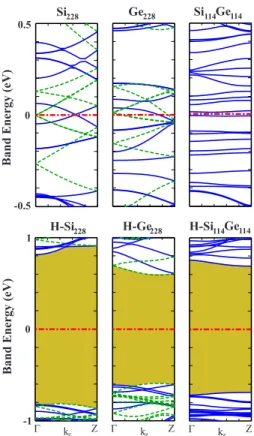
The band structures of optimized bare and hydrogenated SinGenare given in Figs.3 and4for n = 75 and 114, respec-tively. In the same figures, the band structures of bare and hydrogenated Si2n and Ge2n constituent nanowires are
pre-sented for the sake of comparison. SiN 共N=25 and 57兲 and hence any Si2n 共n=sN兲 nanowires are metallic due to the surface dangling bonds. Similarly, GeN 共N=25 and 57兲 and hence any Ge2n are metallic. Upon passivation of dangling
bonds, these metallic nanowires become semiconductor. For example, H-Si150and H-Ge150nanowires have indirect band
gaps, Eg= 1.1 and 0.7 eV, respectively. Normally, the band gap of a H-Sinis inversely proportional to its diameter, if the corresponding ideal nanowire cut from the bulk crystal was directly passivated with H before the structural optimization. Also, the band gap is affected by the cross section geometry for small N. For large N, the variation of Eg with N is more uniform.
Like Si150and Ge150, Si75Ge75is metallic. The ideal
equi-librium ballistic conductances of Si150, Ge150nanowires, and
Si75Ge75NWSL are revealed to be 6e2/h, 10e2/h, and 8e2/h,
respectively. Since H-Si150and H-Ge150are semiconductors, H-Si75Ge75 NWSL is also semiconductor: Its band gap is
0.7 eV and close to the band gap of H-Ge150. H-Si114Ge114
has a direct band gap of 1.4 eV. Again, it is smaller than the
band gap of H-Si228but closer to that of H-Ge228.
In Fig.5, we examine how the electronic energy bands of nanowire superlattices evolve with the lattice constant c or s. In the case of N = 25, bare SinGennanowire superlattices are metallic for all n 共n=25 and 50 or s=1, 2, and 3兲. As s increases, additional minibands occur and they become flat-ter. As for H-SinGen, they are all semiconductor for n = 25, 50, and 75. As n increases, all bands including lowest con-duction and highest valence band become flatter with the formation of minibands. In this respect, the band gap be-comes more uniform as s increases. Similar behaviors are
Band Energy (eV) Band Energy (eV) Si150 Ge150 Si75Ge75
H-Si150 H-Ge150 H-Si75Ge75
0 1 -1 0.5 0 -0.5 Γ kz Z Γ kz Z Γ kz Z
FIG. 3.共Color online兲 Energy band structures of optimized bare and hydrogenated Si2n, Ge2nnanowires, and SinGen nanowire
su-perlattices for n = 75. Zero of energy is taken at the Fermi level. Band gaps are shown by shaded zones. Dashed and dotted lines 共minibands兲 are obtained by folding of Si50共also H-Si50兲 and Ge50 共also H-Ge50兲 bands.
Si228 Ge228 Si114Ge114
H-Si228 H-Ge228 H-Si114Ge114
Band Energy (eV) Band Energy (eV) 0 1 -1 0.5 0 -0.5 Γ kz Z Γ kz Z Γ kz Z
FIG. 4.共Color online兲 Energy band structures of optimized bare and hydrogenated Si2n, Ge2n nanowires, and SinGennanowire
su-perlattices for n = 114. Zero of energy is taken at the Fermi level. Dashed and dotted lines are obtained by folding of Si57 共also H-Si57兲 and Ge57共also H-Ge57兲 bands.
0 -0.5 0.5 n=25 n=50 Γ kz Z Γ kz Z Band Energy (eV) n=25 n=50 1 -1 0 Γ kz Z n=57 n=57
FIG. 5.共Color online兲 Energy band structure of bare and hydro-genated SinGennanowire superlattices for n = 25, 50, and 57.
displayed also for H-SinGenwith n = 57 and 114共see Fig.4兲.
Unexpectedly, bare SinGenare semiconducting for n = 57 and 114. The band gap decreases from 0.27 to 0.02 eV as s in-creases from 1 to 2. Isosurface charge densities of these states near the band gap edges found that they are confined in one of the zones. It is concluded that opening of the band gap originates from the mismatch of surface dangling bond states in Si and Ge zones.
It should be noted that the band gap is underestimated by the GGA calculations used in the present study. GW correc-tion performed recently20 for H-Si
n in different orientations is in the range of 0.5– 0.6 eV for large diameters. In view of the fact that Ge bulk is predicted as metal by GGA calcula-tion, GW correction for H-Gennanowires is expected to be in the same range as that for H-Sin. Under these circumstances, a scissor operation共namely, increasing the band gap of cor-responding SinGen by the same amount of 0.5– 0.6 eV兲 may yield the actual band gap. In summary, the band gaps of H-SinGen predicted by GGA calculation are underestimated, and actual bands are expected to be 0.5– 0.6 eV larger.
VI. CONFINED STATES
The results discussed in the previous section reveal that Sinand Gennanowires making a Si/Ge heterojunction in the supercell have band gaps of different widths. Upon a pseudo-morphic junction, the bands and hence band gaps corre-sponding to Si and Ge zones are aligned. Combination of two features, namely, Si and Ge zones having different band gaps and band lineup, results in band discontinuities and hence band offsets. The conduction and valence band edges of different zones共Si zone or Ge zone兲 in the nanowire su-perlattice will have different energies. Under these circum-stances, the diagram of the conduction band edge along the axis of NWSL will display a multiple quantum well structure with the periodicity of csclike a Kronig-Penny model. Elec-trons in the well region of a zone should decay in the adja-cent zones having higher conduction band edge, since their energy will fall into the band gap of this barrier zone. As a result, the states of these confined共or localized兲 electrons are propagating in the well, but decaying in the barrier. Usually, confined electrons have low group velocity. They may be-come more localized if the barrier is high and the width of barrier is large. If the confinement共or localization兲 is com-plete, the associated band En共kz兲 becomes flat.19 Similar
ar-guments are valid for the hole states if the energies of va-lence band edges of both zones are different.
In the past, the reference energies in determining band offsets of 2D superlattices have been actively studied both experimentally and theoretically. Energy diagrams of con-duction and valence band edges are then used as effective potential forming a multiple quantum well structure.21 The
states of conduction band electrons and holes of valence band were treated using effective mass theory共EMT兲. These states are free electronlike 2D bands in the planes and Bloch states forming minibands perpendicular to the planes. The conditions are, however, different in NWSLs. First of all, EMT may not be applicable directly in the present case, in particular, for NWSLs with small diameter. Second, the
ref-erence energy level determined for planar superlattices may not be appropriate. Recently, Kagimura et al.6proposed
sur-face dangling bond states as reference level for Si/Ge core-shell superlattices. Under estimation of band gaps by DFT, GGA calculation may hinder the accurate determination of band lineups. Voon and Willatzen7drew attention to the
lat-eral confinement of states in NWSLs. Using one-band EMT and by solving the Ben Daniel–Duke22equation, they found
that the effective barrier is lowered due to the coupling be-tween radial and longitudinal confinements. In particular, they predicted that the effective barrier and hence confine-ment disappear below a critical radius of ⬃5 nm. In the present study, the maximum radius of NWSL was ⬃0.9 Å which is much lower than the critical radius set for GaAs/AlGaAs NWSLs.7
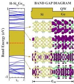
In the present study, we examined whether some of states can be longitudinally confined by performing an extensive analysis of charge densities of superlattice bands calculated by first-principles methods. The formation of periodic quan-tum well structure is schematically described in Fig. 6. We expect that the values of band gaps in the H-Si and H-Ge zones in a unit cell of the H-Si75Ge75cannot deviate
signifi-cantly from the values calculated for periodic H-Si25 and
H-Ge25 nanowires 共namely, 1.1 and 0.7 eV, respectively兲.
When the two zones are connected by an atomically flat in-terface, H-Ge zone can form a well between adjacent H-Si zones, since the band gap of the former zone is smaller and the energy of conduction band edge is lower relative to that of the latter zone. Upon normal band lineup, H-Ge75 zone
acts as a quantum well for both lowest conduction and high-est valence band electrons. Band structure of H-Si75Ge75
with two lowest conduction and two highest valence mini-bands and their isosurface charge distribution in the superlat-tice unit cell are shown in Fig. 6. The distribution of elec-tronic charge density is confirming the above normal band lineup. Both conduction band states are confined in the H-Ge75zone, but they have very small weight in the H-Si75
0 Band Energy (eV) 1 -1 Γ kz Z QW Si Ge
H-Si75Ge75 BAND GAP DIAGRAM
c
scFIG. 6. 共Color online兲 Schematic description of energy band diagram in the unit cell共on the right and upper side兲, band structure in the momentum space共on the left side兲, and isosurface charge density of states of H-Si75Ge75NWSL at the band edges.
zone. Similarly, states corresponding to two highest valence bands are also confined in the H-Ge75 zone. It should be noted that owing to the charge transfer between adjacent zones the form of the energy band diagram may change from the simple form given in Fig.6.
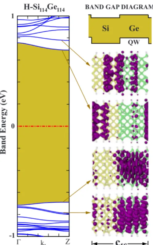
In Fig. 7, we present similar analysis for H-Si114Ge114 NWSL. As compared to H-Si75Ge75, here H-Si and H-Ge
zones are⬃5 Å shorter. However, there are more minibands owing to larger number of Si and Ge atoms. The ways the highest valence band and the lowest conduction band states are confined in different zones suggest a staggered band lineup. Highest valence band states are confined in the H-Ge zone; but lowest conduction band states are confined in H-Si zone. States of sixth and seventh valence bands 共from the top兲 are propagating throughout the NWSL.
We believe that present ab initio results revealing con-fined states for NWSLs with a radius as small as ⬃0.6 nm
are not contradicting the conclusions obtained from one-band EMT model. We think that EMT as applied in Ref.7has to be revised for small diameter NWSL.23 We also note that H-SinGen nanowire superlattice has 1D rodlike structure. There are several minibands in the 1D BZ. The number of minibands in a given energy interval increases with either increasing N 共i.e., increasing diameter兲 or increasing s. A nanowire superlattice with a long unit cell having several Si or Ge atoms will have several共quasi continuous兲 minibands. States of H-Sinor H-Gen zone of the same energy are more likely to match each other to construct a state that propagate throughout the NWSL. Otherwise, a superlattice of small radius with short unit cell has small number of bands. Then, the states in different zones are less likely to match. A state, which cannot find a matching partner, is confined to its zone. As a matter of fact, we were able to deduce confined states even in the barrier zone共H-Si兲 with energies higher than the conduction band edge.
VII. CONCLUSION
Atomic structure of H-Sin and H-Gennanowires is tetra-hedrally coordinated near the center, but at the surface devi-ates significantly from corresponding bulk crystal. Calcu-lated force constants indicate that Sin is stiffer than Gen. Generally, nanowires become stiffer after passivation with hydrogen. These two nanowires are 1D semiconductors with their band gap depending on their diameter and also on the geometry of their relaxed cross section. If finite segments of these nanowires are joined pseudomorphically and the result-ing heterostructure are repeated periodically along the axis of the wires, one obtains a H-SinGen superlattice structure. In these longitudinal NWSLs, electrons are normally bound to the wire in radial direction, but propagate along their axis. A specific state which propagates in one zone共say H-Si兲 can decay in the adjacent zone 共say H-Ge兲, when a matching state in the same energy is absent. Such a state is called confined state. Our charge density analyses indicate that Si/Ge NWSL with radius as small as 0.6 nm can have con-fined states at the band edges and also within the conduction and valence band. Confined states offer interesting device applications. NWSL has an important advantage that the de-vice part and leads can be produced from similar nanowires. Theoretically, NWSLs have several interesting issues to be clarified. In particular, theories derived from planar superlat-tices to predict band lineups and model calculations using EMT have to be revised for small diameter NWSLs.
1M. T. Bjork, B. H. Ohlsson, T. Sass, A. I. Persson, C. Thelander, M. H. Magnusson, K. Deppert, L. R. Wallenberg, and L. Sam-uelson, Nano Lett. 2, 87共2002兲.
2M. S. Gudiksen, L. J. Lauhon, J. Wang, D. C. Smith, and C. M. Lieber, Nature共London兲 415, 617 共2002兲.
3Y. Wu, R. Fan, and P. Yang, Nano Lett. 2, 83共2002兲.
4L. J. Lauhon, M. S. Gudiksen, D. Wang, and C. M. Lieber, Nature
共London兲 420, 57 共2002兲.
5R. N. Musin and X.-Q. Wang, Phys. Rev. B 71, 155318共2005兲. 6R. Kagimura, R. W. Nunes, and H. Chacham, Phys. Rev. Lett. 98,
026801共2007兲.
7L. C. Lew, Yan Voon, and M. Willatzen, J. Appl. Phys. 93, 9997 共2003兲.
8F. R. Zypman, Phys. Rev. B 71, 165313共2005兲.
9O. Gulseren, T. Yildirim, and S. Ciraci, Phys. Rev. B 68, 115419
H-Si114Ge114 Γ kz Band Energy (eV) 0 1 -1 Z Si Ge
BAND GAP DIAGRAM
csc
QWFIG. 7. 共Color online兲 Schematic description of energy band diagram in the unit cell共on the right and upper side兲, band structure in the momentum space共on the left side兲, and isosurface charge density of states of H-Si114Ge114NWSL at the band edges.
共2003兲; C. Kilic, S. Ciraci, O. Gulseren, and T. Yildirim, ibid.
62, R16345共2000兲.
10M. C. Payne, M. P. Teter, D. C. Allen, T. A. Arias, and J. D. Joannopoulos, Rev. Mod. Phys. 64, 1045共1992兲.
11Numerical computations have been carried out by using VASP
software: G. Kresse and J. Hafner, Phys. Rev. B 47, R558 共1993兲; G. Kresse and J. Furthmuller, ibid. 54, 11169 共1996兲. 12W. Kohn and L. J. Sham, Phys. Rev. 140, A1133 共1965兲; P.
Hohenberg and W. Kohn, Phys. Rev. 136, B864共1964兲. 13D. Vanderbilt, Phys. Rev. B 41, R7892共1990兲.
14J. P. Perdew, J. A. Chevary, S. H. Vosko, K. A. Jackson, M. R. Pederson, D. J. Singh, and C. Fiolhais, Phys. Rev. B 46, 6671 共1992兲.
15M. Methfessel and A. T. Paxton, Phys. Rev. B 40, 3616共1989兲. 16H. J. Monkhorst and J. D. Pack, Phys. Rev. B 13, 5188共1976兲. 17M. Menon, D. Srivastava, I. Ponomareva, and L. A.
Chernozaton-skii, Phys. Rev. B 70, 125313共2004兲.
18These calculations have been performed by minimizing the total energy under a preset uniaxial strain in the elastic range. The strains on Ge and Si zones calculated are determined after full relaxation.
19Accordingly, such a state has 兰
well⌿c*⌿cdrជ Ⰷ兰barrier⌿c*⌿cdrជ . If
the confinement is complete, electrons in adjacent levels do not interact. This is known as the Mott localization.
20X. Zhao, C. M. Wei, L. Yang, and M. Y. Chou, Phys. Rev. Lett.
92, 236805共2004兲.
21L. Esaki and L. L. Chang, Phys. Rev. Lett. 33, 495共1974兲. 22G. Bastard, Wave Mechanics Applied to Semiconductor
Hetero-structures共Les Editions de Physique, Les Ulis, 1988兲.
23We also note that the material parameters of GaAs/AlGaAs rel-evant for EMT by themselves are different from SinGen