STRUCTURE OF У
âl® ï B ï
m
шші
ттш
» r a M ï » M a r i 'M
ршіш шштт
ші
ш
іттшттп
ш і ш т ш ё ш M & ÿ m т г ш ш » т "j Í 11?2ί üύ
L S Ь Й^
1 vi 5-7 Wk. V ; w w __ELECTRONIC STRUCTURE OF LOW DIMENSIONAL
SEMICONDUCTOR SYSTEMS
A THESIS
SUBMITTED TO THE DEPARTMENT OF PHYSICS AND THE INSTITUTE OF ENGINEERING AND SCIENCE
OF BILKENT UNIVERSITY
IN PARTIAL FULFILLMENT OF THE REQUIREMENTS FOR THE DEGREE OF
DOCTOR OF PHILOSOPHY
By
Oguz Giilseren
July 1992
(UÜİlİG
Λ ■6|l / (з
' S 3
1 certify that I have read this thesis and that in my opinion it is fully adequate, in scope and in quality, as a dissertation for the degree of Doctor of Philosophy.
Prof. Dr. Salim Çıracı (Supervisor)
I certify that I have read this thesis and that in my opinion it is fully adequate, in scope and in quality, as a dissertation for the degree of Doctor of Philosophy.
I certify that I have read this thesis and that in my opinion it is fully adequate, in scope and in quality, as a dissertation for the degree of Doctor of Philosophy.
I certify that I have read this thesis and that in my opinion it is fully adequate, in scope and in quality, as a dissertation for the degree of Doctor of Philosophy.
. S '.
Prof. Dr. Şinasi Ellialtioğlu
I certify that I have read this thesis and that in my opinion it is fully adequate, in scope and in quality, as a dissertation for the degree of Doctor of Philosophy.
Prof. Dr. M. Cemal Yalabık
Approved for the Institute of Engineering and Science;
Prof. Mehmet Bar ay,
Abstract
ELECTRONIC STRU CTU RE OF LO W DIM ENSIONAL
SEM IC O N D U CTO R SYSTEM S
Oğuz Gülseren
Pli. D. in Physics
Supervisor: Prof. Dr. Salim Çıracı
July 1992
Recent progress made in the growth techniques has led to the fabrication of the artificial semiconductor systems of lower dimension. Electrons and holes in these materials have quantization different from those of the three dimensional systems presenting unusual electronic properties and novel device applications. In this work, the important features of the free carriers in semiconductor superlattices are examined, and the electronic structure of some novel 2D semiconductor systems are investigated theoretically. This thesis studies various systems of lower dimensionality such as: the strained Si/Ge superlattices, i-doping. Si (100) surface and the tip-sample interaction in scanning tunneling microscopy (STM) study of this surface, and Wannier-Stark localization in finite length superlattices.
The electronic energy structure of pseudomorphic Ge„i/Si„ superlattices is investigated by using the empirical tight binding method. Effects of the band offset, sublattice periodicity and the lateral lattice constant on the transition energies have been investigated. It is found that Ge„i/Si„ superlattices grown on Ge (001) can have a direct band gap, if m + n = 10 and m = 6. However, optical matrix elements for in-plane and perpendicular polarized light are negligible for
the transition from the highest valence band to the lowest conduction band state at the center of the superlattice Brillouin zone.
The electronic structure of the Si i-layer in germanium is explored by using the Green’s function formalism with layer orbitals. We found two dimensional parabolic subbands near the band edges. This approach is extended to treat the electronic structure of a single quantum well without invoking the periodically repeating models. Quantum well formation in Ge,„Si„ superlattices is also studied by using different number of ^-layers. Subband structure is observed by changing the height of the Si quantum well.
The confinement of acoustical modes within 2DEG due to only the electron- phonon interaction is proposed. The confined modes split out from the bulk phonons, if the 2DEG is created by means of modulation doping. This occurs even if the lattice has uniform parameters. The effect is more pronounced when the wave vector q of the modes increases and is maximum a,t q = 2kp {kp is the Fermi wave vector). In the case of several electron sheets the additional features of the confinement effect appear.
Green’s function method is also applied to treat the modifications of electronic state density in STM. The tip-sample interaction in STM study of Si (100) surface is explored by calculating the Gieen’s function within the empirical tight binding method. Both of the proposed reconstruction models, buckled and symmetrical dimer model, is investigated. A dip occurs in the change of density of states of surface atoms at the energy of surface states for small tip-sample distances, and it decreases with increasing tip-sample separation. Although, in-plane tip position (above the up- or down-surface atom) affects the surface atoms differently in buckled dimer model, it influences the surface atoms symmetrically in symmetric dimer model.
Recent experimental studies revealed the significant information on the Wannier-Stark localization. Following these experimental results, the Wannier- Stark ladder is investigated by carrying out numerical calculations on a multiple quantum well structure under an applied electric field. The variation of the Wannier-Stark ladder energies and localization of the corresponding wave
function are examined for a wide range of applied electric field. Our results show that Wannier-Stark ladder do exist for finite but periodic system which consists of a large number of quantum well having multi-miniband structure. It is found that the miniband states are localized in the well regions with the applied electric field, while the continuum states preserve their extended character. Energies of the well states show a linear shift with the electric field except the small field values in which a nonlinear shift is resulted. Multiband calculations show that there is a mixing between the different band states although they are localized in different well regions.
K ey w ord s: Superlattice, quantum well, mismatch, strained superlattice, deformation potential, optical transition, empirical tight binding method. Green’s function, layer orbital, ^-doping, acoustical phonon confinement, electron-phonon interaction, scanning tunneling microscopy, tip-sample interaction, surface reconstruction, Wannier-Stark ladder, Wannier-Stark localiza tion.
özet
DUŞUK BO YU TLU YAR IİLETKEN SİSTEMLERİN
ELEKTRONİK YAPISI
Oğuz Gülseren
Fizik Doktora
Tez Yöneticisi: Prof. Dr. Salim Çıracı
Temmuz 1992
Büyütme tekniklerindeki son geli.şmeler düşük boyutlu yapay yarıiletken sistemlerinin üretimini sağlamıştır. Bu malzemelerde bulunan serbest elektron ve boşluklar üç boyutlu sistemlerdekine göre farklı bir kuantumlaşma ile alışılmamış elektronik özellikler göstererek yeni aygıt uygulama alanlarına yol açmaktadırlar. Bu çalışmada, yarıiletken süperörgülerindeki serbest taşıyıcıların önemli nitelikleri anlatıldı ve bazı 2 boyutlu yarıiletken sistemlerin elektronik yapısı kuramsal olarak incelendi. Bunlar gerilmiş Si/Ge süperörgüleri, 8- katkılama, Si (100) yüzeyi ve bu yüzeyin tarama tünelleme mikroskobu ile incelenmesinde ki uç-örnek etkileşimleri ve sınırlı uzunluktaki süperörgülerde Wannier-Stark yerelleşmesi olarak sıralanabilir.
Gerilmiş Ge„ı/Si„ süperörgüleriiiin elektronik yapısı, denemesel sıkı bağlanma yöntemi kullanılarak çalışıldı. Kuşak süreksizliği, alt-örgü periyodu ve yatay örgü değişmezinin geçiş enerjileri üzerine etkileri incelendi. m + n = 10 ve rn = 6 iken Ge (001) üzerine büyütülmüş Ge„ı/Si„ süperörgülerinin direk kuşak aralığı olabileçeği bulundu. Öte yandan, süperörgü Brillioun bölgesinin merkezinde, en yüksek değerlilik kuşağından en düşük iletkenlik kuşağına olan geçişlerin düzlem
içi veya dik polarize olmuş ışık için optik matris elemanlarmm çok küçük olduğu bulundu.
Germanyum içindeki Si ¿-tabakasının elektronik yapısı tabaka orbitalleri ile yazılmış Green fonksiyonu ile incelendi. Kuşak kenarlarında iki boyutlu parabolik alt-kuşaklar bulundu. Bu yaklaşım, periyodik yinelenen modelleri kullanmadan tek kuantum kuyusunun elektronik yapısını hesaplamak için de geliştirildi. Değişik sayıda ¿-tabakası kullanarak Ge,„Si„ süperörgülerinde kuantum kuyusu oluşumu çalışıldı. Silisyum kuantum kuyusunun yüksekliği değiştirilerek alt- kuşak yapısı gözlendi.
iki boyutlu elektron gazında (2BEG), sadece elektron-fonon etkileşiminden dolayı akustik modların sınırlanması öne sürüldü. Örneğin modulasyon katkılama gibi bir yolla yaratılan 2BEG’da sınırlanmış modlar düzgün örgü özelliklerinde bile bulk fononlarmdan ayrılırlar. Bu etki, modların dalga vektörü q ile artar ve <7 = 2kp {kp Fermi dalga vektörüdür) iken en yüksek olur. Birçok elektron tabakası bulunduğu durumda sınırlanma etkisinin değişik özellikleri gözükür.
Si (100) yüzeyinin tarama tünelleme mikroskobu ile incelenmesi ve uç.-örnek etkileşimleri Green fonksiyonu yöntemi ile araştırıldı. Kuşak hesaplamalarında denemesel sıkı bağlanma metodu kullanıldı. Asimetrik ve simetrik dimer yüzey yeniden yapılanına modellerinin her ikiside incelendi. Küçük uç-örnek uzaklıklarında, yüzey atomlarının durum yoğunluklarının değişiminde, SN, yüzey durum enerjilerinde bir düşme gözlendi. Bu düşme, uç-örnek uzaklığı artıkça azaldı. Uç atomunun aşağıdaki veya yukarıdaki yüzey atomunun üzerinde olması AA^’ni asimetrik dimer modelinde farklı etkilerken, simetrik dimer modelinde simetrik bir değişim gözlendi.
Son deneysel çalışmalar Wannier-Stark yerelleşmesi üzerinde önemli bilgiler vermiştir. Bu çalışmaları göz önüne alarak, elektrik alan uygulanmış süperörgü yapılarında sayısal hesaplamalar ile Wannier-Stark merdiveni incelendi. Geniş bir elektrik alan aralığında, Wannier-Stark merdiveni enerjilerinin değişimi ve karşılık gelen dalga fonksiyonlarının yerelleşmesi araştırıldı. Sonuçlarımız, çok sayıda kuantum kuyusu ve çok kuşak içeren sınırlı periyodik sistemlerde Wannier- Stark merdiveninin bulunduğunu gösterdi. Mini-kuşak durumlarının elektrik
alan uygulanmasıyla kuantum kuyularında yerelleştiği bulundu. Bu durumların enerjileri elektrik alanı ile doğrusal bir kayma gösterdi. Fakat, küçük alan değerlerinde doğrusal olmayan bir kayma bulundu. Çok kuşak hesaplamaları, değişik kuyu bölgelerinde sınırlanmalarına karşın değişik kuşak durumlarının karıştığını göstermiştir.
Anahtar
sözcükler: Süperörgü, kuantum kuyusu, örgü uyuşmazlığı, gerilmiş süperörgüler, deformasyon potensiyeli, optik geçişler, den- emesel sıkı bağlanma yöntemi, Green fonksiyonu, tabaka orbitali, i-katkılama, akustik fonon sınırlanması, elektron- fonon etkileşimi, tarama tünelleme mikroskobu, uç-örnek etk ileşimi, yüzey yeniden yapılanması, Wannier-Stark merdiveni, Wannier-Stark yerelleşmesi.
Acknowledgement
I would like to express my deepest gratitude to Prof. Salim Çıracı for his supervision to my graduate study. He introduced me the fascinating world of the condensed matter theory. His guidance and encouragement plays the major role in my physics education. I benefited a lot from his enthusiastic and friendly supervision.
I appreciate Dr. Erkan Tekman for his valuable discussions and comments during my graduate study.
I am grateful to the members of the Physics Department. The discussions with them in formal and informal seminars help me a lot.
I would like to thank Prof. V.A. Kochelap. I learned the Russian way of thinking from him.
I bless a lot to our secretaries Mrs. Dilek Kaynaroglu and Mrs. İmren Koçak for their logistical support and for special parties with cookies.
My sincere thanks are due to my family for their continuous moral support. Last but not the least, I owe a great dept of thanks to my wife Hülya who has stood by me and supported me well beyond the call of duty.
Preface
Low dimensional systems in Condensed Matter Physics have led several novel features with interesting applications in electronic technology. It is hoped that microelectronics, photonics and computer technology will benefit extensively from the recent progress made in this field.
In this thesis, the electronic structure of some 2D semiconductor systems is investigated theoretically. This study includes the electronic structure of strained Si/Ge superlattices and ^-doping, tip-sample interaction in scanning tunneling microscopy of Si (100) surface, and Wannier-Stark localization in finite length superlattices.
The organization of this thesis is as follows. In Chapter 1, important aspects of condensed systems of lower dimensions are outlined. Chapter 2 is devoted to the electronic structure of strained Si/Ge superlattices. Green’s function and perturbation theory is reviewed in Chapter 3, and then it is used in the study of 8- doping and tip-sample interaction in STM of Si(lOO) surface. A new confinement effect of acoustical modes in the presence of ¿-doping is proposed in Chapter 3. Electric field effects on finite length superlattices is investigated in Chapter 4. A brief conclusion is given in Chapter 5.
Contents
Abstract i Özet iv Acknowledgement vii Preface viii Contents ix List of Figures xiList of Tables xiv
1 Novel Features of the Condensed System of Lower Dimensional
ity 1
1.1 Properties of Multilayer Semiconductor S y stem s... 1
1.2 Electronic Structure 8
1.3 Superlattices... 14
2 Electronic Structure of Strained S i/G e Superlattices 16
2.1 Strained Layer Superlattices... 16
2.2 Electronic Structure of Si-Ge (001) Superlattices 22
2.2.1 Tetragonal Distortion... 24 2.2.2 Brillouin Zone F o ld in g ... 27
2.2.3 Si/Ge Superlattices Grown on Si(0 0 1 )... 29
2.2.4 Si/Ge Superlattices Grown on G e (O O l)... 35
2.A Empirical Tight-binding M ethod... 51
2.B ETB Energy Bands of Diamond S tr u c tu r e ... 52
3 Green’s Function Approach for the Electronic Structure of 2D Systems 65 3.1 Green’s Function and Perturbation T h e o r y ... 65
3.2 Green’s Function for the Systems with 2D P eriodicity... 71
3.3 i- d o p in g ... 72
3.3.1 Electronic Structure of Si ¿-layer Embedded in Ge (001) . 73 3.3.2 Confinement of Acoustical Modes due to the Electron-phonon Interaction within 2 D E G ... 78
3.4 Modifications of Electronic State Density in Scanning Tunneling Microscopy ... 91
3.4.1 Reconstructed Si(lOO) 2 x 1 Surface... 92
4 Electric Field Effects on Finite Length Superlattices 101 4.1 Overview of Theory and Experiments... 102 4.2 Wannier-Stark Ladder on Finite Length Superlattices... I ll
5 Conclusions 125
Bibliography 129
List of Figures
1.1 Quantum well structure and real space energy band structure 2 1.2 Subband structure and density of states in 2D s y s t e m s ... 4 1.3 Energy band diagram for n-doped (modulation doped) superlattices 6 1.4 Resonant tunneling model for heterostructures... 7 1.5 Bistability in resonant tunneling d io d e s ... 8 1.6 Discontinuities of band edge energies of three kinds of hetero
interfaces ... 9 2.1 Energy gaps versus lattice constants at 4.2 K ... 17 2.2 Critical layer thickness as a function of misfit p a r a m e te r ... 20 2.3 Minimum band gap of Gei..Sii_a,. as a function of germanium fraction 21 2.4 Band structures for .Si and Ge... 24 2.5 FCC Brillioun Z o n e ... 25 2.6 Schematic description of the tetragonal d isto r tio n ... 25 2.7 Schematic description of tetragonally distorted superlattice . . . . 26 2.8 Folding of Si-like indirect band stru ctu re... 28 2.9 Electroreflectance spectrum of Si4/G e4 superlattice grown on Si (001 ) 29 2.10 Unit cell and Brillouin Zone of Si„/Ge,I (001) superlattices . . . . 31 2.11 Energy band structures of Sig(OOl), Ges(OOl) and Si4/Ge4(001)
s tru ctu re s... 33 2.12 AFg of Si„/G e„ superlattices as a function of superlattice
periodicity n... 35 2.13 Electroreflectance spectra of Si4/Gee and Si3/G e7 ... 36 2.14 Constant energy surfaces of conduction band minima of Si . . . . 37
2.15 Variation of some energies of Si2o and Ge2o as a function of parallel lattice c o n s ta n t ... .39 2.16 Variation of the relevant transition energies of Ge„i/Si„ with the
number of the Ge layers m ... 44 2.17 Energy band structure of GeeSi.) and Ge7.Si3 strained superlattices
grown on Ge (001)... 45 2.18 Variation of the transition energies with respect to the band offset 47 2.19 Transition energies as a function of ац in Ge,„Sin strained
superlattices... 50 2.20 Diamond S tru ctu re... 53 3.1 Energy band structure of Si4-G e (001)... 74 3.2 A N {E ), change in density of states at Г point for Si4-G e (001) . . 75 3.3 Energy band structure of Si4-G e (001) for different band offset
values A E „... 77 3.4 Characteristics of confined modes as a function of wave vector q
for single electron sheet at different tem p era tu res... 87 3.5 Phase velocity ui/qci as a function of wave vector q for two identical
electron sheets at two different temperatures... 90 3.6 Top view of some of the possible Si (100) surface... 93
3.7 Side view of dimer models of the Si (100) surface 94
3.8 Side view of Si (100) with tip ... 96 3.9 Surface states of Si (100) (2 x 1) s u r f a c e ... 97 3.10 Change in LDOS in asymmetric dimer model for different tip
positions at Г p o in t ... 99 3.11 Change in LDOS in symmetric dimer model for different tip
positions at Г p o in t ... 100 4.1 The electric field potential energy decomposed into ¡ieriodic and
nonperiodic co m p o n e n ts ... 106 4.2 Electric field absorption coefficient at 24 К ... 107 4.3 Conduction and valence band potential profiles at different electric
fie ld s ... 108
4.4 Photocurreiit (PC) spectra at different electric fields... 109
4.5 Transition energies versus electric f i e l d ... 110
4.6 Potential energy diagram for a finite periodic s y s t e m ... 112
4.7 Potential energy diagram for a non-zero electric f i e l d ... 114
4.8 The fan diagram for the finite length s u p e rla ttice ...115
4.9 The squared amplitude of the wave fu n c t io n ...116
4.10 Localization of the 4'^* well state as a function of normalized electric field... 117
4.11 The absolute square of the wave function of the two anticrossing states ... 119
4.12 Localization of the 4‘^‘ well state versus the electric field at larger buffer layer length...121 4.13 The squared amplitude of the wave function in multi-band analysis 123
List of Tables
2.1 Properties of silicon and germanium... 23
2.2 Lattice parameters and band line-ups for Si/Ge interfaces 27
2.3 Selected experimental deformation potentials of silicon and germa nium ... 41 2.4 Optical transition energies and matrix elements in GegSi^ and
GerSia superlattices... 49
Chapter 1
Novel Features of the Condensed
System of Lower Dimensionality
1.1
Properties of Multilayer Semiconductor
Systems
The novel properties discovered in the electron systems of lower dimensionality’ ”^ have created a major impact in physics and electronics. The properties of a condensed system are strongly dependent on its d im e n sio n a lity .P ro g re s s in growth techniques made it possible to produce various systems with lower dimensionality. Lower dimensionality indicates a system with an effective dimension less than three, such as 2D, ID or OD. Effective dimension 7i means that the carriers are free to move in n dimensions while their motion is constrained in remaining (3 — n) dimensions.
Quantum well wires which have diameters of the order of 10“ ^ m is an example of ID electron systems. In such a wire structure, the electrons are confined to move along the direction of wire while the motion normal to the wire is quantized in the remaining two dimensions. Sakaki’’ pointed out that the electrons can exhibit very high mobilities because of the suppression of the elastic scattering by ionized impurities in GaAs-Gai.^-ALAs quantum wires.
Chapter 1. Condensed System of Lower Dimensionality
AlAs
Ga,_^Alj(As GaAs
AlAs Ga,.)(AI)( As
F igu re 1.1: Quantum well structure and real space energy band structure
Two dimensional (2D) electron systems are the ones in which the components of the system are free to move in two spatial dimensions, but have their motion constrained in the third dimension. In other words, the electrons or holes have quantized energy levels for one spatial dimension, but are free to move in two spatial dimension. Thus, the wave vector is a good quantum number for two dimensions, but not for the third one.
The junctions between insulators and semiconductors such as Si:Si02, semi conductor heterostructures and semiconductor superlattices can be considered as examples of 2D systems. A simple picture of a semiconductor heterostructure, say Gai_xAliAs-GaAs-Gai_a;Ali-As (or semiconductor superlattice), has been described within an effective mass approximation (see figure 1.1). For example, the GaAs sublattice having lower conduction band and higher valence band edges as compared to the adjacent Gai-^ AU-As sublattice can be viewed as a potential well (or multiple potential wells). In this ca.se, the depths of these quantum wells for the motion of electrons and holes become discontinuities in the conduction and valence band, respectively. Excess carriers, i.e. electrons or holes confined in this ID potential well are assumed to have a free particle like character in
a plane perpendicular to the confinement direction, and display a quasi two dimensional (2D) behavior/ They have quantization different from those of the three dimensional (3D) systems, which leads to new effects such as the normal and fractional quantum Hall effects. Several novel features in these superlattice structures, which are of significant importance in device applications, have recently been discovered. For example, by using modulation doping techniques it is now possible to confine the impurities in the barrier region and carriers in the wells so that scattering by the impurity centers is avoided. In this way, carrier mobilities at low temperature have been increased enormously, and the response times of devices have been lowered down to picoseconds. Currently, the study of the properties of carriers of lower dimensions has been a major effort of the fundamental and applied research. In addition to these, many other systems show two dimensional character such as intercalated graphite and thin films.
Chapter 1. Condensed System of Lower Dimensionality
3
Mo l e c u l a r Be a m Ep i t a x y
Advances in epitaxial growth techniques, especially molecular beam epitaxy (MBE), have made possible the preparation of structures with superlattice periodicity ranging from a few tens of nanometer down to the width of a monolayer.*’^ Epitaxy is the growth of layers of semiconductor materials on a substrate with perfect continuity of lattice planes through all interfaces. MBE also leads to highly controlled characteristics such as chemical composition, dopant concentration and profile, as well as thickness uniformity. Under ultra- high vacuum (UHV) conditions, thermal atomic and molecular beams are directed to the heated single crystal substrate. Co-evaporated constituent elements of the epitaxial layer and dopants react chemically with the heated crystalline substrate. Due to the slow growth rate of 1 monolayer/second, changes in composition and doping can be abrupt on the atomic scale. For the cost of UHV (clean environment) and slow growth rate we get precisely processed atomic scale heterostructures.
Chapter 1. Condensed System o f Lower Dimensionality
Tm/itn
E, E.
F igure 1.2: Subband structure and density of states in 2D systems
Qu a n t i z e d Le v e l s a n d Su b b a n d St r u c t u r e
Since the effective mass Schrödinger equation leading to the envelope function has a ID potential along the z-direction (which is perpendicular to the layers) it can be separable for the spatial coordinates lying in the growth planes (x y - plane) and in the z-direction. The solution in the xy-plane have free electron eigenstates. The solution in the direction perpendicular to the layers leads to a set of discrete energy levels. Then the energy eigenstates are
D — Ell T
2m':{K + K ) (1.1)
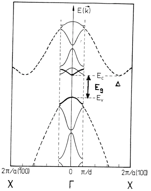
where and ky are the wave vector components for motion parallel to the surface and the En are the electronic quantum levels arising from confinement in the potential well. The confined electron states form subbands, which are identified by their minimum values, E„ (n=l,2,3,...) as shown in figure 1.2. If the potential barriers are wide enough, the interaction between the states confined in adjacent wells is negligible. So the solutions are considered as quantum well states. In contrast, the interaction between wells in a periodic structure causes the discrete quantum levels of widely spaced wells to be replaced by a series of energy bands called minibands of superlattices. The widths of these energy bands increase as the width and height of the potential barrier decrease. The superlattice periodicity gives rise to a new, smaller Brillouin zone in the k^
direction. Certainly, this is a very simplified picture of the confined states, which assumes parabolic conduction and valence bands of the parent semiconductors and wide quantum wells. Advanced theories have to be used to treat the electronic structure accurately, and to resolve its crucial feature, however.
Qu a n t u m Ha l l Ef f e c t
One of the interesting properties seen in 2D systems is the quantum Hall effect, integer or f r a c t i o n a l . K . von Klittzing performed the Hall experiment on a silicon field effect transistor in which the free electrons are confined within a thin layer. He found that behaviour of the electrical resistance and the Hall resistance were dramatically different from the ordinary Hall measurements when the devices are cooled down to ~ O^K and placed in a strong magnetic field. The Hall resistance, instead of increasing steadily and linearly with the strength of the magnetic field, exhibits a series of plateaus, and becomes quantized to values where i/ is an integer. Electrical resistance drops to zero in the same interval of the magnetic field, where the Hall resistance exhibits plateaus. In a two dimensional electron system a magnetic field perpendicular to the plane of electrical confinement leads to a new quantization which yields sharp Landau levels separated by the cyclotron energy fiUc. A quantized Hall resistance is resulted if the carrier density (which is usually assumed to be fixed in measurements) and the magnetic field are adjusted in such a way that the filling factor 1/ of the energy levels is an integer. In a GaAs/AlAs heterojunction
fractional values are also observed.
Chapter 1. Condensed System of Lower Dimensionality
5
Ex c t t o n s
Excitons in a system of lower dimensions exhibit also unusual behaviours. Excitons in semiconductors do not survive at room temperature, because their binding energies are too small and thus become ionized by thermal phonons. In quantum well structures with widths smaller than the Bohr radius, the structure of excitons are modified. Confined exciton flattens and shrinks. Compression on
Chapter 1. Condensed System o f Lower Dimensionality
Donor
F igu re 1.3: Energy band diagram for n-doped (modulation doped) superlattices
the exciton increases the binding energy and hence stabilizes the structure. This stability makes the observation at the room temperature possible. The room temperature excitonic resonances in a quantum well structure offers a convenient way of making use the large, intensity dependent adsorption and reflection effects. Nowadays, the bistability effects arising therefrom is considered as a potential tool for optic computing. Moreover, in layered structures or quantum well structures 2D character leading to the subband structure and thus the step-like density of states (see figure 1.2) increases the number of states contributing to the optical transitions at the adsorption edge. Adsorption spectra of quantum well structures are significantly different from the constituent semiconductors. This is used for very low threshold diode lasers.
Mo d u l a t i o n Do p i n g
Semiconductor quantum well structure also provides new opportunities in doping. Modulation d o p i n g ' i s one way to enhance mobilities in heterostructures. As seen in figure 1.3, in this method, barrier regions are doped while the well regions are not. Donors in the barrier layers are ionized and electrons go from barrier region to the well regions where they become confined. This way, carriers and impurity ions being physically separated, the impurity scattering, which is the only mechanism lowering the mobility at low temperature, is avoided. Measured mobilities parallel to the layers are much larger than those of uniformly doped structures. Mobility values 2 — 3 x I tf cm^/Vsec is achieved as T —> 0*'K. This is almost 2-3 orders larger than mobilities obtained in Si technology.
Cha.pter 1. Condensed System o f Lower Dimensionality
Ga,.,Ai,As
2ZZ3
E.
Metal GaAs Melal
N
2 ZZ
ZZ5
F igu re 1.4: Resonant tunneling model for heterostructures
Re s o n a n t T u n n e l i n g
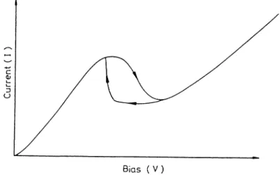
Another interesting application of 2D systems is the resonant tunneling.*®’^® Consider an undoped Gai-x AR-As-GaAs-Gai-ajACAs heterostructure as shown in figure 1.4. Under a small positive bias applied to the electrode on the right, the tunneling probability is small, and so is the current between two electrodes. When the bias applied to the structure is such that the energy of the quantum state E„ coincides with the Fermi energy of one of the electrodes, resonant tunneling occurs and the tunneling current increases dramatically. Upon further increasing the bias, the matching of the energies E/r and E„ is destroyed, and hence the resonant tunneling changes to normal tunneling. At very high bias, one of the barriers effectively disappears and the current increases again. The bistability which is o b s e r v e d , i n the I-V characteristic of a resonant tunneling diode is not a single valued function as shown in figure 1.5, and it can be an important property for the memory device applications. Although either the space-charge
Chapter 1. Condensed System o f Lower Dimensionality
Figure 1.5: Bistability in resonant tunneling diodes
buildup in the resonant level or the external circuit oscillations are found to be responsible from the bistability, there is no consensus about the origin of this p h e n o m e n o n . P o s s i b l e technological applications of resonant tunneling are quantum well oscillators at frequencies up to 18 GHz, room temperature negative resistance, persistent photocarriers in quantum well resonators.
1.2
Electronic Structure
In a semiconductor heterostructure or in a semiconductor superlattice the band offset is the most important feature affecting the electronic ])ioperties obtained t h e r e o f . F o r each parent semiconductor the average of the crystal potential and the energy of the valence band maximum with respect to this average potential have different value. Moreover, the electronegativities of the atoms exhibit a large amount of variation by going from one semiconductor to another. Accordingly, when two different semiconductors (for example GaAs and AlAs) are put in an intimate contact, the top of the valence bands occur at different energies leading to a natural band lineup. Owing to the difference in the electronegativities of the interface atoms belonging to the different semiconductor sublattices, one expects a transfer of charge which in turn creates a dipole field across the i n t e r f a c e . As a result the bands of the adjacent sublattices may exhibit a relative
Chapter 1. Condensed System o f Lower Dimensionality Ec,. Ev, Ec. Ev, AEc rx,,.,A(,As AEv TH lype I (Straddling) AEc Ge {aEv Type II (Staggered ) AEc InAs GaSb AEv -EV2 ■ tC2 •Ev, ■Ec, • Ev, Type II ( M isaligned)
Figure 1.6: Discontinuities of band edge energies of three kinds of hetero interfaces
shift, and thus a dramatic increase of the total energy. At the end, the offset of the valence band, AEy, is stabilized by the alignment of the charge neutrality levels, which corresponds to the minimum of the total energy of the heterostructure at hand. Since the band gaps of the parent semiconductors (Egi,Eg2) are different,
the offset of the conduction bands is given by AEc = Egi — Egi — AEy.
Semiconductor heterojunctions are classified into three groups, as described in figure 1.6. These are Type I (straddling). Type Il-staggered, and Type ITmisaligned. GaAs/Gai_i.Al,;As heterojunction is an example of a type I junction. In this structure, carriers, both electron and holes, are confined in GaAs sublattice. On the other hand, in the type Il-staggered heterojunctions, for example Si/Ge, while electrons are confined in one sublattice (Si-sublattice),
Chapter 1. Condensed System of Lower Dimensionality
10
holes are confined in the other one (Ge-sublattice). In the same way, type Il-misaligned heterojunctions, InAs/GaSb heterojunction, show the same confinement behaviour as staggered ones. However, in these superlattices the energy gap decreases with the increasing period to result in a semiconductor- semimetal transition.
In addition to the band offset the electronic energy structure of the semiconductor superlattices are modified by the zone folding due to the new periodicity imposed by the superlattice structure. While the translational periodicity is maintained in the xy-plane of a lattice matched heterostructure, the lattice periodicity along the z-direction is altered and becomes the periodicity of the superlattice. As a result, the reciprocal lattice vector along the z-axis, and thus the superlattice Brillouin zone (SBZ) in the same direction becomes shorter as compared to their parent values in constituent bulk semiconductors. The zone folding has significant effects in the semiconductor heterostructures, for which the difference of the direct and indirect gap, AEdi = E^^^ — E^’\ is large. For example, the indirect gap of Si crystal, which occurs along the FX-direction of the fee BZ, ~ 2 eV below the direct gap, is folded near to the center of BZ in the Si/Ge superlattice grown along the [001] direction.
The electronic structure of the layered semiconductors leading to the quantum well structures have been investigated theoretically by using several different methods. The simplest of these is the method based on the effective mass approximation. The one electron hamiltonian of the whole system can be written as2 6.
rc
(1.2)
where U{r) denotes the crystal potential. If r lies in the sublattice A
U{f) = otherwise U{f) = U^{r). Expanding the wave functions having and kf/ (A.’x, ky, 0)
- '^Cn^{k,)xnk{i^ (1.3)
Chapter 1. Condensed System o f Lower Dimensionality
11
i k f X „ t(0 = e (1.4) with t/,f„(r) z ,A U^„(f) zeBbeing the band edge eigenfunctions at ^ = 0, one obtains the envelope function, which is the Fourier transform of Cni/{kz)·, from the following effective mass Hamiltonian
h 1 h'^k^//
' m{z) " ' ^ \ ' 2m(z)
The z-dependent effective mass is defined by 1 (1.5) m{z) m ^ (0) - E,f,(0) and 1 _ 1 m.{z) m V < t'.?o|v|c,fo > ,k n E.?(o) - £.?(o) for zeA for zeB (1.6) (1.7) In the above effective mass equation
V(z) = (1.8)
An extensive discussion of the above method, and the approximations used therein can be found in Reference 2,26-31.
While the methods based on the effective mass approximation works well for simple parabolic band edges and thick quantum wells, its validity becomes questionable when the size of the well becomes small (~ 10Á). As the width of the well is reduced the energy levels of the confined states may experience dramatic shifts. This is the well known quantum size effect. Apparently, the small periodicity semiconductor superlattices have to be treated by more rigorous methods.
In the tight binding method, dimension of hamiltonian matrix increases with the size of the unit cell because of the using of local orbital basis. Since the interface destroys translational symmetry in the perpendicular direction, the unit cell size becomes infinite. To overcome this computational difficulty, a
Chapter i. Condensed System o f Lower Dimensionality
12
slab with a finite thickness repeated in the perpendicular direction to create an artificial supercell is i nt r oduc ed. Anot her approach is the reduced hamiltonian method which is suggested for solving the tight binding equations for interfaces. In this method, a transfer matrix is introduced to relate the electronic wave functions on different planes parallel to an interface. So the knowledge of the wave function on a small number of adjacent planes is sufficient to determine the wave function on all other planes. Then an expansion in bulk states with complex wave vector values is made. Heterojunction is modelled as the combination of three regions. There are two bulklike regions and between them a region of interfacial distruption. Compositional grading from one semiconductor to t,he other is represented by a layer dependent weighted average of the tight binding parameters of the two semiconductors. Finally, an iterative method is used for finding energy eigenvalues.
Jaros and his coworkers^^’'^® developed a method, which uses the wave functions of the parent, bulk semiconductors obtained within the empirical pseudopotential method. Their method is essentially similar to the effective mass approximation, and starts with the hamiltonian of one sublattice, which is connected by the difference potential, V, to the adjacent sublattice. Pseudopotentials are determined from the optical data. The wave function of the superlattice is expanded in terms of bulk Bloch states.
(1.9)
n,ki
The components of each wave function specify the degree of participation of the individual bulk Bloch states in forming the superlattice state. Using the completeness and orthonormality of Bloch state, the Schrödinger equation can be transformed into:
- E)
+ E A.,i <
>= »
7 1,
(1.10)
The superlattice eigenvalues and eigenfunctions are calculated from the diago- nalization of this secular matrix. As one notices, in this method the band offset has to be implemented in the calculations.
Chapter 1. Condensed System of Lower Dimensionality
13
The energetics (i.e. stability, interface geometry, and the energy optimized atomic structure e.t.c.) and the band lineup of the small periodicity semiconductor superlattices have been treated accurately by using ab-initio calculations. The rearrangements of the atoms due to the internal strain imposed by the lattice mismatch, and the interface dipole field created by the charge transfer occurring as a result of the electronegativity difference affect the electronic structure in an essential manner. Consequently, a realistic description of the electronic properties requires the determination of the quasi equilibrium position of the atoms trapped in a local minimum in the Born-Oppenheimer surface. The ab-initio methods provides the calculation of the interface geometry and energy optimized atomic structure. Moreover, the stability of the superlattice relative to the different structures or relative to the disproportionation into parent semiconductors is extremely important for the degradation. Presently, the ab-
initio calculations seem to be the only way to investigate the stability. The quasi
equilibrium structures have been also searched by the molecular dynamics studies even though the empirical potentials used in these calculations are questionable. Since the charge distribution is self-consistently calculated, the band lineup is also determined from the first principles in the ab-initio methods.
Presently, the SCF pseudopotential method in momentum representation is the most successful ab-initio method to investigate the energetics and the electronic s t r u c t u r e . S i n c e the exchange and correlation effects are treated within the local density approximation, the energies of the conduction band states are underestimated in the SCF-pseudopotential calculations. Recently, by applying many body self-energy corrections it has been shown that even the accurate conduction band energies can be obtained.'^* An extensive review of electronic structures of semiconductor heterostructures can be found in Reference 39-41.
Chapter 1. Condensed System o f Lower Dimensionality
14
1.3
Superlattices
Clearly, semiconductor superlattices present new conceptual ideas about syn thetic semiconductors, and new device applications. A semiconductor superlat tice (S i)„/(S2)m provides many degrees of freedom for controlling the electronic properties of this system. These are basically the repeat periods {rn,7ia7idm + n), and the sublattices (Si and S2) themselves. The repeat periods (i7i-|-?i) determines the subband structure, confinement of states, and band alignment. Si and S2 have similar lattice parameters, but different electronic structure. Sometimes they can be replaced by the alloy (Si )i_a;(S2)a; which yield continuously varying properties. In this way the band gap and the band offset of the superlattice can be monitored to engineer the quantum wells. In the growth and in the overall character of a heterostructure, the polarity of the sublattices. Si and S2, play a crucial role, which leads to more fundamental classifications. These are polar-polar, polar- covalent and covalent-covalent heterostructures.
Consider GaAs/Gai_j; Ali-As semiconductor superlattice as an example. While GaAs has a direct band gap of ~ 1.4 eV, AlAs is an indirect band gap semiconductor with a smallest gap of 2.3 eV. The band gap of Gai-i-AU-As alloys varies between 1.4 eV and 2.3 eV depending upon the value of A1 composition. Since GaAs and AlAs have almost the same lattice parameter, GaAs/Gaa,.Ali_iAs superlattice is a lattice matched heterostructure. It allows device applications with very low power consumption and very high switching speeds.
It is also seen that the electronic structure depends strongly on the superlattice periodicity n, when n is small. For example, while (GaAs)„/(AlAs),i has a type-I band discontinuity, the confined electron and hole states are separated in direct and momentum space for 71 = 4, as if it has a staggered tyj^e-II band offset.
In Si„/Ge,i (n > 3) the direct, indirect gap decreases with increasing 71. The
difference between the direct and indirect gap is positive but recedes to 0.07 eV for n = 6.
Semiconductor superlattices present new conceptual ideas about novel device applications. Devices fabricated from these synthetic semiconductors have
Chapter 1. Condensed System o f Lower Dimensionality
15
high electron mobility, very short response times, and low power consumption. In addition to their excellent optical properties, some of the semiconductor superlattices (for example GaAs/AlAs, perhaps S i„/G e„) are capable of combining electronics with photonics.
Chapter 2
Electronic Structure of Strained
S i/G e Superlattices
The dislocation-free, strained-layer siiperlattices involving thin layers of semi conductors with large lattice mismatch can be grown^·^“^^ with molecular beam epitaxy. In this context, it is hoped that pseudomorphic Si-Ge superlattices can compensate for the shortcomings of silicon and can open new horizons in the applications of Si-based devices in photonics. In this chapter, electronic structure of strained Si/Ge superlattices will be investigated.
2.1
Strained Layer Superlattices
Active research on layered structures such as superlattices results in valuable improvements on device ¡jhysics. In such structures, to avoid the defects at the interface it is necessary to use materials with similar crystal structures and nearly same interatomic distance. In epitaxial growth of crystalline .semiconductor films crystallinity and orientation are determined by the substrate. Heteroepitaxy is named for the growing of different atomic layers on top of each other. Hence, for defect free growth, matched lattice structures and lattice constants are essential.
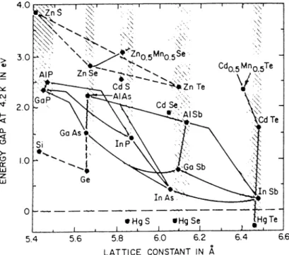
A large number of quantum well systems are achieved with advanced epitaxial growth techniques. Figure 2.1 shows the plot of energy gaps at
Chapter 2. Electronic Structure o f Strained Si/Ge Superlattices
17
Figure 2.1: Energy gaps versus lattice constants at 4.2 K From reference 5
4.2K versus lattice constants for zinc-blende .semiconductors together with Si and Ge. .joining lines represent ternary alloys. Superlattices and quantum wells or heterojunctions grown with pairs selected from those materials, include IiiAs/GaSb(/AlSb), InAlAs/InGaAs,®'^ InP/lattice matched alloys,51-54 Ge/GaAs,55.56 CdTe/HgTe,^^'5"’58 PbTe/PbSnTe,59.60 ZnS/ZnSe,5i-52 and ZnSe/ZnTe.4® On the other hand, silicon has a small lattice constant (5.43
A)
which is closely matched by only three other common semiconductors: GaP, AlP, and ZnS as seen in figure 2.1. These materials consist of the elements which are effective at generating free carriers in silicon, but not in germanium. Although germanium has the same crystalline structure with silicon, its lattice constant is about 4% larger. Therefore, Si/Ge superlattice is a pseudomorphic system which leads to strained layers. A lot of work was also done on strained layer systems parallel to the lattice matched ones.Strained layer systems are important for the following r e a s o n s . F i r s t of all, semiconductor structures can be grown pseudomorphically on foreign
Chapter 2. Electronic Structure o f Strained Si/Ge Superlattices
18
incommensurate substrates. Silicon substrates offer properties superior to other semiconductor materials with regard to wafer size, crystal perfection, thermal conductivity, handling and price. But silicon has a small lattice constant (5.43
A)
which is approximately 20% smaller than that of group IV,III/V and II/VI semiconductors. Secondly, there is a great increase in the number of possible superlattice systems with inclusion of lattice mismatched semiconductor pairs. Lastly, strain modifies the band structure of superlattice systems which provides additional parameter to control the electronic properties.Nowadays, it is possible to grow the dislocation-free, strained-layer super lattices involving thin layers of semiconductors with large lattice mismatch. Consider an epilayer with lattice constant Oep, and substrate with lattice constant
(isubs- Lattice mismatch parameter / is defined as
/ = (^epi ^^subs
^subs (
2
.1
)The lattice mismatch can be accommodated in two ways: elastic accommodation by strain and plastic accommodation by misfit dislocations lying in the interface. Therefore, the lattice mismatch parameter / can be written as
/ — e + - V
(2.2)
where e is elastic strain, b is length of Burgers vector and p is distance between misfit dislocations.*^'* Hence, misfit dislocations reduce the strain. The important parameter of pseudomorphic strained layer systems is the critical thickness
he- The epilayer can be grown without the introduction of misfit dislocations
(strained layer epitaxy, pseudomorphic or commensurate growth) up to a certain thickness which is named as critical thickness he- Therefore, beyond the he misfit dislocations reduce the strain. The critical thickness he can be found from the thermodynamical equilibrium theories.*^'^“*^® The equilibrium theories of growth of pseudomorphic strained layers are based on the assumption of that the layers are in mechanical equilibrium. There are two basic approaches. The condition of minimum total energy is suggested by van der Merve,*^^ while the force balance is by Matthews and Blakeslee.*’*^’*^^
Chapter 2. Electronic Structure of Strained Si/Ge Superlattices
19
The total energy Et is the sum of homogeneous strain energy E^ and energy of misfit dislocation
EfU-Et = Ek ^— Eds (2.3)
P
where n is the number of dislocations.*^® In the elastic continuum theory, the energy Eh due to strain in the epilayer grown on Si(lOO) is®“*
Ek = 2/i
1 — // (2.4)
where p is the shear modulus, // is Poisson’s ratio, e is the elastic strain and h is the thickness of the epilayer. The strain energy Eds of a single dislocation is®“*“®®
Eds = l + l n (
-Vi (2.5)
47t(1 + n) .
where R is the range of a dislocation line and 7·,· is inner cut-off radius for the dislocation core. Very thin layers up to he grow without misfit dislocations requires
kl = / ) P — ^ when h < he (2.6)
The critical thickness he can be found from the minimization condition of equation 2.3 as
b
he l^i + 1„ (2.7)
87t(1 + i/)f
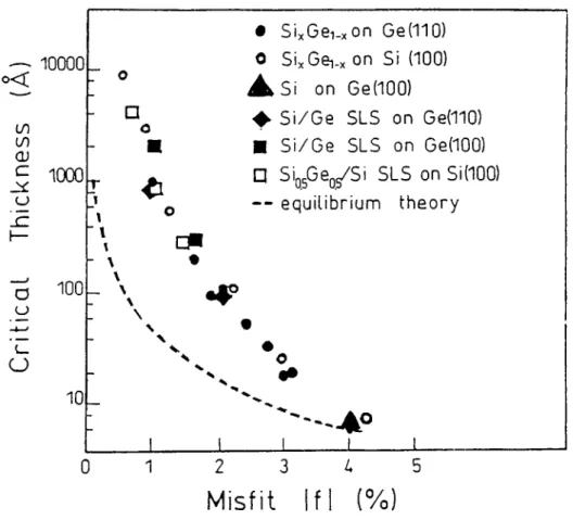
for the growth on the (100) surface of a crystal of diamond structure. Figure 2.2 shows the critical layer thickness for strained-layer epitaxy of GeSi on Si and Ge as a function of misfit parameter.
Similarly, in the case of strained layer superlattice, mismatch between layers are accommodated by elastic strain. The mismatch between the layers is
/ = 9-” '^ ~ (2 .8 )
«1 + 0,2
where ai and ai are the lattice constants of the corresponding layers. The elastic strains 6i and ti in the superlattice layers satisfy the relation
Chapter 2. Electronic Structure of Strained Si/Ge Superlattices
20
o < Li) m 0)c
u 10000 a o lI u r o 1000 100 10_□
} \ \ \ \ \ u \ # SixGei-xOn GedIO) 0 SixGe^.x on Si (100) Jkk S i on GedOO) ^ Si/G e SLS on Ge(IIO) ■ Si/G e SLS on Ge(IOO) □ SiQ^Ge^/Si SLS on Si(IOO) — equilibriunn theory • r 2 3Misfit
fl (%)
Figure 2.2: Critical layer thickness as a function of misfit parameter
From Reference 70
if there is no misfit dislocations in the superlattice interfaces. For pseudomorphic growth
h\
, /l'2 < /ic(fl>C2)
(2.10)
The critical thickness of individual superlattice layers can be found from equation 2.7 by inserting strains ci and C2 instead of
Another important aspect is the modifications in the superlattice band structure due to the strain. The strain is such that the band diagram of these structures is not just perturbed but changes considerably. The biaxial stress cr in the layers can be described as the sum of a hydrostatic pressure and an uniaxial
Chapter 2. Electronic Structure o f Strained Si/Ge Superlattices
21
F igu re 2.3: Minimum band gap of GexSii_a; as a function of germanium fraction From Reference 47
From Reference 47
stress normal to the layers.'^ / cr 0 0 ^
0
a 0
0 0 0 y(T 0 0 \
0
(7
0
0 0 cr y +/
0
0
0
^
0
0
0
^ 0 0 —<T y (2
.11
)The hydrostatic part simply shifts the conduction and valence bands up and down depending on the sign of the pressure, while the uniaxial part leads to some splittings/’ Working with strain hamiltonians and deformation potentials results that the band gaps of Gea,Sii_a; and Si depend strongly on the relative allocation of s t r a i n . A detailed description will be given later. Figure 2.3 shows the calculated results for the minimum bad gaps of several materials as a function of the atomic fraction of germanium. The two-dimensional electron systems with enhanced low-temperature mobilities'^ was also observed in Si/Sii_iGex
Chapter 2. Electronic Structure o f Strained Si/Ge Superlattices
22
strained-layer superlattices. An extensive bibliography about SiGe strained systems is given in reference 73.
2.2
Electronic Structure of Si—Ge (001)
Superlattices
Its excellent etching and mechanical properties have made silicon an indispensable material in microelectronics technology. On the other hand, being an indirect-gap semiconductor, silicon has been excluded from photonics and optoelectronics. Improving electronic properties of this crystal has been the continuing effort of material scientists. Recent progress in the fabrication of epitaxial semiconductor superlattices with multiple quantum well structure providing novel two-dimensional (2D) electronic properties has stimulated the idea of increasing carrier mobility in Si/Ge heterostructures by modulation doping. In an effort to compensate for the deficiencies of silicon and to further upgrade this well established technology the epitaxial growth of pseudomorphic Si/Sii-^Ge^; heterostructures has been a c h i e v e d . R e c e n t l y , the growth of pure Ge ( x =l ) up to six layers pseudomorphically restricted to Si(OOl) substrate has been realized by Pearsall and his c o l l a b o r a t o r s . M o r e importantly, they observed direct optical transitions in the (Si)4/(G e)4 semiconductor superlattices grown on the .Si(OOl) substrate, which are found neither in constituent crystals nor in the Sio.sGeo.s alloy. This result has been an encouraging step towards making Si a direct band gap semiconductor appropriate for photonics.
Pr o p e r t i e s o f Si a n d G e
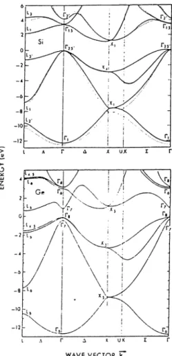
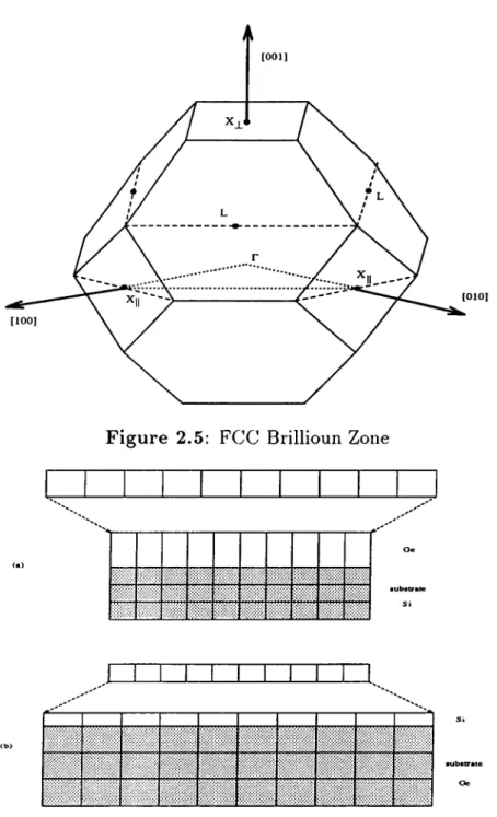
The physical properties of silicon and germanium are summarized in table 2.1. The band structures of Si and Ge obtained from the pseudopotential calculation are shown in figure 2.4. The labels in the band diagram is indicated in fee Brillioun zone presented in figure 2.5. Critical directions for SiGe strained superlattices is also shown in figure 2.5. Silicon crystal has six minima along
Chapter 2. Electronic Structure o f Strained Si/Ge Superlattices
23
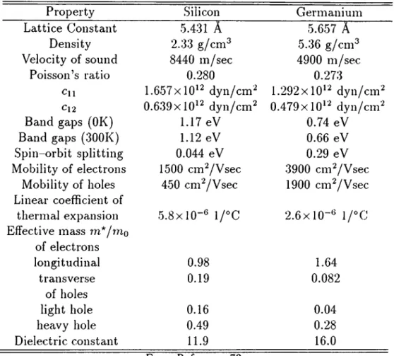
Table 2.1: Properties of silicon and germanium
Property Silicon Germanium
Lattice Constant 5.431 A 5.657 À
Density 2.33 g/cm^ 5.36 g/cm®
Velocity of sound 8440 m/sec 4900 m/sec
Poisson’s ratio 0.280 0.273
Cll 1.657x10^^ dyn/cm^ 1.292x10’ ^ dyn/cm^
Cl 2 0.639x10^^ dyn/cm^ 0.479x10*'^ dyn/cm^
Band gaps (OK) 1.17 eV 0.74 eV
Band gaps (300K) 1 .1 2 eV 0.66 eV
Spin-orbit splitting 0.044 eV 0.29 eV
Mobility of electrons 1500 cm'^/Vsec 3900 cm^/Vsec
Mobility of holes 450 cm^/Vsec 1900 cm^/Vsec
Linear coefficient of
thermal expansion 5.8x10-® 1/°C 2.6x10-® 1/°C
Effective mass m*/mo of electrons longitudinal 0.98 1.64 transverse 0.19 0.082 of holes light hole 0.16 0.04 heavy hole 0.49 0.28 Dielectric constant 11.9 16.0 From Reference 73
the A-direction of BZ denoted by the A*-states. The resulting experimental band gap is indirect and 1.1 eV. The direct band gap is large, and the energy difference between the direct and indirect band gap, AEg, is ~ 2 eV. Also Ge is an indirect band gap semiconductor, except that the conduction band minima occur at the four L-points of BZ. While Si and Ge are indirect band gap material, commensurate, strained-layer Si-Ge superlattices can be direct band gap material owing to the zone-folding and strain imposed by the lattice mismatch. The following is discussion of electronic structure of strained Si/Ge superlattices.
Chapter 2. Electronic Structure o f Strained Si/Ge Superlattic.es
24
Figure 2.4: Band structures for Si and Ge. From Reference 75
2.2.1
Tetragonal Distortion
Figure 2.6 is a schematic description of strained layer system. When there is a lattice mismatch between the lattices, the sublattice grown in registry with the substrate undergoes a compressive (expansive) strain while the lattice constant in the perpendicular direction expands (contracts) leading to a tetragonal distortion if Uepi > Usubs {«-epi < (hubs)· As a result, the strain distorts the cubic lattice cell to a tetragonal cell. Almost continuously adjustable lateral lattice constant (by using .Sia;Gei_a; alloy) and the lattice strain generated thereof is an essential ingredient of the strained Si-Ge superlattices.
Chapter 2. Electronic Structure of Strained Si/Ge Superlattices
25
Figure 2.5: FCC Brillioun Zone
I I I I I I
■ubBtr«i
Oc
F igu re 2.6; Schematic description of the tetragonal distortion
surface as seen in figure 2.7. The strains and the lattice parameters can be found by minimizing the total elastic energy. The in-plane lattice parameter a||
Chapter 2. Electronic Structure of Strained Si/Ge Superlattices
26
substrate
Figure 2.7: Schematic description of tetragonally distorted superlattice
of the superlattice becomes^^
_ (ISjhsiMsi + (iGehaeMge , .
""" “ hsiMsi + ha^Mae ^ ^
where 05,· and acje are lattice constants of Si and Ge respectively, and /15, and
hoe are the thickness of Si and Ge layers. Mi is the shear modulus given as for
(100) direction
/ ^2 \
(2.13)
Mi — 2 I cn + C12 — 2—
V
^
1 1. .
where i denotes the different materials. Two limits of equation 2.12 is found easily, ay = asi when hsi/hae —>■00, This corresponds to a Si substrate with strained Ge on top of it. Similarly, for Ge substrate hadhsi 00 and in-plane lattice constant becomes ny = aoe- Actually, the value of ay is determined by the substrate, i.e. is equal to the lattice constant of the substrate, and may be varied by using different substrates. Once ay is known, perpendicular lattice parameter can be found from
a ,i = a,· 1 - 2 ^ c’u
ay - a,
ai (2.14)
The lattice parameters for Si/Ge system were calculated within this macroscopic approach by Van de Walle et And then beginning with these values they
Chapter 2. Electronic Structure of Strained Si/Ge Superlattices
27
Table 2.2: Lattice parameters and band line-ups for Si/Ge interfaces
«II (À) «.Six (À) «G'eX (A) AEy (eV) AEy^av (eV) AEy (eV)
5.4.3 5.43 5.82 0.84 0..54 0.28
5.52 5.36 5.75 0.61 0.53 0.41
5.65 5.26 5.65 0.31 0.51 0.55
AEy = Ey^Oe ~ Ey^si is the discontinuity in the top of the valence band;
AEy^av = Ey^Oe,av ~ Ey^si,av ¡s the discontinuity in the average of the valence bands;
AEc = Ec,Oe — Ec,si is the discontinuity in the minimum of the conduction band.
performed full self-consistent pseudopotential calculations for total energy and forces. The result for the lattice parameters were within the 1% of the found from equation 2.12 and 2.14. The results of Van de Walle^'’^* for lattice constant with band line-ups is summarized in table 2.2.
Parallel and perpendicular strain components can be found from the ratios of lattice constants ^ ^ _ ^11 ~ ^XX ^yy --üi and (2.15) ^ z _L _.,£12 — ^ ^XX (2.16)
2.2.2
Brillouin Zone Folding
The periodicity of a superlattice d is much larger than the one of bulk materials
a. Hence, the superlattice ])eriodicity creates a new, smaller Brillouin zone in the k; direction ( z is the superlattice growth direction).
7T , 7T
(2.17) The first superlattice Brillouin zone can be constructed by folding the Brillouin zone of the bulk crystal into first minizone. It was proposed^® that the zone folding effect can transform an indirect band gap to a direct band gap. An
Chapter 2. Electronic Structure of Strained Si/Ge Superlattices
28
r
X
Figure 2.8: Folding of Si-like indirect band structure From Reference 70
example of the folding of host crystal Brillouin zone of a Si-like indirect band structure to a superlattice Brillouin zone (supei'lattice periodicity is five times the bulk periodicity, d = 5a) is shown in figure 2.8. For example, the conduction band minimum of bulk Si which occurs at | k |ci 1.67r/a along A-direction can be folded to the center of the zone if the superlattice periodicity along [001] increases
Chapter 2. Electronic Structure of Strained Si/Ge Superlattices
29
UJ O Z < ÜJ tr O cr UJ "1 I I I \ 1 r 9 I ! 8 ; : ■ r ! ■ \ ' / \ i “ I I r~l I i T" \l :/\tt ' I I ■ M I ■ y ■ !l .■■■·! |,t;-i··: ·♦> r · ^ \ /»■>·' (Ge4;S¡4)x5 SUPERLATTICE I 1I I I I 0.5 10 15 2.0 2.5 ENERGY (eV) 3.0 I 1 1. L 1.-3.5 (a) 4.0F igure 2.9: Electroreflectaiice spectrum of 814/064 superlattice grown on Si (001)
From Reference 74
by a factor of 5. Therefore, it is possible to get a direct band gap by folding an indirect band gap structure.
2 .2.3
S i/G e Superlattices Grown on Si(OOl)
In a Si,i/Ge,i superlattice restricted to the (001) surface of Si the lattice mismatch of 4% is completely accommodated by the uniform lattice strain in the commensurate or pseudomorphic Ge layers. Recently, the growth of the pure Ge(i.e. a: = I) up to six layers restricted to the Si(OOl) surface unit cell have been a c h i e v e d . N o v e l electronic properties of these strained Si,i/Ge„(001) superlattices have been reported^^’^'*’" ” '^ promissing new device applications. For example, Pearsall et observed direct optical transitions at 0.76, 1.25, and 2.51 eV which were found neither in the constituent crystals (i.e. Si and Ge), nor in the Sio.sGeo.s alloy. Electroreflectance spectrum of Si4/G e4 superlattice grown on Si (0 0 1) is shown in figure 2.9. Hoping to use the well developed Si technology in optoelectronics, especially in laser applications, motivated the studies on strained Si/Ge systems.