Analysis and design of a 3.5 ghz patch antenna for wimax applications
Tam metin
Şekil
![Table 1.1 Current major spectrum allocations for WiMAX worldwide [5]. Region Frequency Bands (GHz) Comments Canada 2.3, 2.5 3.5 5.8 USA 2.3, 2.5 5.8 Central and South America 2.5 3.5 5.8](https://thumb-eu.123doks.com/thumbv2/9libnet/4039759.56725/14.892.230.731.180.731/current-spectrum-allocations-worldwide-frequency-comments-central-america.webp)


Benzer Belgeler
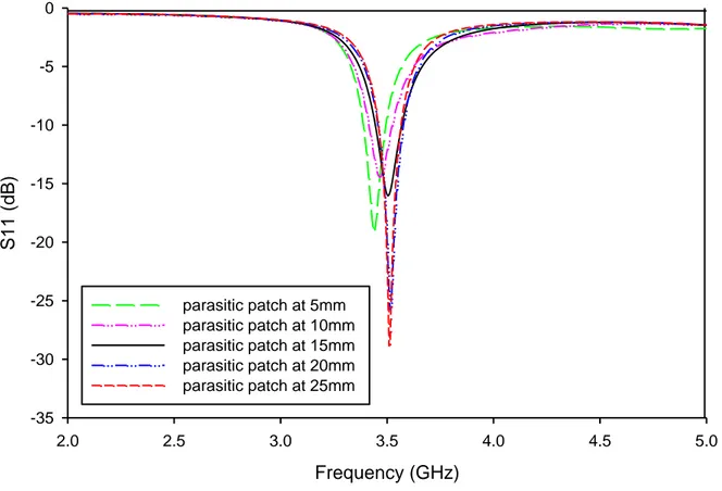
This model is used in section 2.2 to design a rectangular patch antenna and the designed antenna’s simulation results are presented in section 3.2.. 2.2
Ancak bu tedavi modaliteleri arasında metastaz yapmasa da lokal olarak nüks riski yüksek (%19-77) olduğu için cerrahi ola- rak tümörün geniş rezeksiyon ile çıkartılması
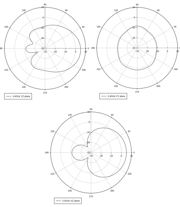
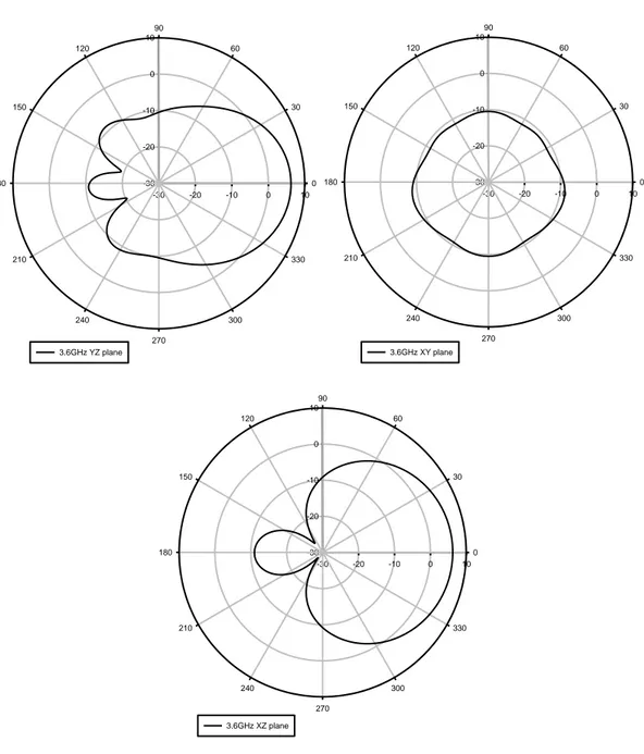
Antenna radiation pattern is measured between ±50° using a manually turning setup with a 25 dBi gain horn
First, the design procedure of 2-D surface to forbid the propagation of transverse magnetic (TM) surface waves in a grounded dielectric substrate around antenna's operative
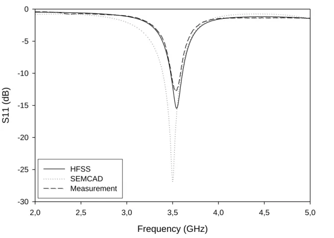
Note that wider bandwidths can easily be obtained by using a thicker substrate. In Figure 8, the simulated and measured return losses of the antenna are shown for the band of 5.6
Once, a good matching is obtained for the inner patch, a good matching impedance can be obtained for the outer patch that will work at 2.4 GHz by moving the inner patch position
The phased antenna array has four microstrip patch antennas, three Wilkinson power dividers and a transmission line phase shifter printed on the dielectric substrate with
2x2 UHF RFID antenna array system at 867 MHz, which consists of phase shifter, power dividers and microstrip patch antenna is designed, implemented and measured. The main beam of
