P H Y S I C S
Electrically control amplified spontaneous emission
in colloidal quantum dots
Junhong Yu1*, Sushant Shendre1*, Weon-kyu Koh1, Baiquan Liu1, Mingjie Li2, Songyan Hou3,
Chathuranga Hettiarachchi4, Savas Delikanli1, Pedro Hernández-Martínez1,
Muhammad Danang Birowosuto3, Hong Wang3,4, TzeChien Sum2,
Hilmi Volkan Demir1,2,5†, Cuong Dang1,3,4†
Colloidal quantum dots (CQDs) are highly promising materials for light amplification thanks to their efficient photoluminescence, tunable emission wavelength and low-cost synthesis. Unfortunately, CQDs are suffering from band-edge state degeneracy which demands multiple excitons to achieve population inversion. As a result, non-radiative Auger recombination increases the lasing threshold and limits the gain lifetime. Here, benefiting from the negative charging, we demonstrate that the amplified spontaneous emission (ASE) threshold is controllable in a device where CQD film is exposed to an external electric field. Specifically, singly charged CQDs lower the threshold due to the preexisting electron in the conduction band, while strongly enhanced Auger recombination in doubly charged CQDs stymies the ASE. Experimental results and kinetic equation model show that ASE threshold reduces 10% even if our device only charges ~17% of the CQD population. Our results open new possibilities for controlling exciton recombination dynamics and achieving electrically pumped CQD lasers.
INTRODUCTION
Since colloidal quantum dots (CQDs) were first demonstrated as an optical gain medium for lasing applications, the search for CQDs with low gain threshold has been hindered by nonunity degeneracy of the band-edge states (1–6), which means that multiple-exciton gain is needed to achieve light amplification (7, 8). This condition requires that the average number of excitons per CQD is greater than one (〈N〉 > 1), signifying that a considerable percentage of CQDs should contain at least one biexciton. This results in the accelerated nonradiative Auger process (9–13), whereby electron-hole recombination energy is nonradiatively transferred to a third carrier. Auger recombination is almost two orders of magnitude faster than the radiative process in typical CQDs (4, 14–16), which has been the main obstacle to achieve sustainable and low-threshold CQD lasing.
Multiple strategies have been proposed to overcome this challenge and achieve low-threshold CQD lasers. Much work has pursued the idea of suppressing Auger recombination. This nonradiative Auger rate (inverse of Auger lifetime) can be reduced by engineering the wave function confinement of electrons and holes in CQDs including type II CQDs (17), alloyed core-shell interface CQDs (18), and “giant” or tailored CQDs (19). Another effort to reduce the optical gain threshold is to inject electrons into the conduction band, i.e., negatively
charged CQDs. These extra electrons contribute to the carrier pop-ulation in the excited state of the CQDs, substantially reducing the reabsorption (optical loss) or even creating optical transparency at the emission wavelength (20). Therefore, the population inversion or stimulated emission can be obtained at much lower pumping levels (6).
Very recently, Klimov’s group has demonstrated population inversion with the optical pumping threshold at 〈N〉 = 0.02 in charged CQDs via photochemical reduction (6). In addition, Guyot-Sionnest’s group had investigated the lowering amplified spontaneous emission (ASE) threshold in CQDs by electrochemical charging at low tem-perature (13). However, photochemical doping requires CQDs in an oxygen-free environment; otherwise, all these changes are reversed completely (20). In addition, the electrochemical method demands a solution (electrolyte) environment to charge CQDs. Given the final goal of achieving a practical CQD laser, a method to charge CQDs reliably in an optoelectronic device is preferred (16). The use of an electric field to modulate the spontaneous emission properties of nanoparticles in a capacitor had been explored by Delehanty’s group (12) and Woggon’s group (21) as a “device-ready” approach. To date, the investigation remaining in the spontaneous regime might be used for sensing applications. Here, we demonstrate the control of CQDs’ ASE in the device structure via electric field–induced charging. By adjusting the voltage bias on the device, we are able to regulate the average charging level in the CQD film, and a lower ASE threshold is achieved with opti-mum charging level where the advantages of low-population inver-sion threshold dominate the adverse effect of Auger recombination.
RESULTS AND DISCUSSION
Spontaneous emission of CQDs in the device
We investigated CdSe/CdS/ZnS core-shell-shell CQDs, which were produced using a slightly modified synthesis recipe (1) reported by Bawendi’s group (see details in Materials and Methods). This quasi– type II structure, shown as an inset in Fig. 1A, has advantages of suppressed Auger rate, high quantum yield (QY), and enhanced
1LUMINOUS! Centre of Excellence for Semiconductor Lighting and Displays, School of Electrical and Electronic Engineering, Nanyang Technological University, 50 Nanyang Avenue, 639798 Singapore, Singapore. 2School of Physical and Mathe-matical Sciences, Nanyang Technological University, 639798 Singapore, Singapore. 3CINTRA UMI CNRS/NTU/THALES 3288, Research Techno Plaza, 50 Nanyang Drive, Border X Block, Level 6, 637553 Singapore, Singapore. 4Centre for OptoElectronics and Biophotonics, School of Electrical and Electronic Engineering & The Photonics Institute, Nanyang Technological University, 639798 Singapore, Singapore. 5 Depart-ment of Electrical and Electronics Engineering and DepartDepart-ment of Physics, UNAM– Institute of Materials Science and Nanotechnology, Bilkent University, Bilkent, Ankara, 06800, Turkey.
*These authors contributed equally to this work.
†Corresponding author. Email: [email protected] (H.V.D.); hcdang@ntu. edu.sg (C.D.)
Copyright © 2019 The Authors, some rights reserved; exclusive licensee American Association for the Advancement of Science. No claim to original U.S. Government Works. Distributed under a Creative Commons Attribution NonCommercial License 4.0 (CC BY-NC).
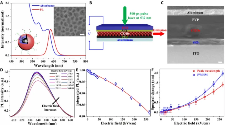
absorption cross section, which are beneficial for laser applications. The high-bandgap ZnS shell with a thickness of ~1.5 nm passivates the potential surface traps and still maintains the quasi–type II structure. The absorbance and photoluminescence (PL) spectra of the diluted CQDs dispersed in toluene (1 mg/ml) at room tempera-ture are presented in Fig. 1A. The PL spectrum [full width at half maximum (FWHM) of ~34 nm] is broader than that of typical CdSe/CdS CQDs, which is attributed to the ZnS outermost shell as widely discussed in the literature for this core-shell-shell structure (9, 18). Both the two well-resolved excitonic transitions and a clean emission spectrum with more than 70% QY suggest the high quality of CdSe/ CdS/ZnS CQDs. High-concentration CQDs (>100 mg/ml) in toluene were prepared for subsequent spin-cast compact CQD films.
We used a capacitor structure to apply electric field on our CQD film. To avoid CQDs being directly adjacent to electrodes, which would quench the photon emission, the CQD film was sandwiched between two dielectric layers [SiO2 and poly(4-vinylphenol) (PVP);
see the Device fabrication section in Materials and Methods]. Meanwhile, this multiple-layer capacitor structure limits the electrical current (see measured current in fig. S6) through the CQD film to a maxi-mum extent. This is important as electric current through a photo-conductive device can lead to heavy charging and result in totally quenched emission of CQDs (22). Figure 1B illustrates the schematic of the device’s layer structure and the excitation geometry for optical
characterization. Accordingly, the spectroscopic modulation observed in our device is attributed to the applied electric field. A sinusoidal AC bias is applied to introduce the external electric field through two electrodes [indium tin oxide (ITO) and aluminum] attached to the top and bottom dielectric layers. The AC bias was chosen to avoid slow chemical processes happening reversibly with the DC bias (see more details in section S1). The thickness of each layer is determined by cross-sectional imaging of the capacitor structure by scanning electron microscopy, as shown in Fig. 1C, which is in good agreement with the measurement by a surface profiler (see thickness results in fig. S2). Given the three layers between the two electrodes, the device is equivalent to three capacitors in series; a reference capacitor is adopted to measure the voltage drop across the CQD film (the detail of the calculation is presented in fig. S1). Together with the measured thickness of the CQD film, the electric field can be ob-tained more accurately for the CQD layer.
The emission properties of the CQD film under the external electric field were investigated by using a subnanosecond pulse laser with a stripe excitation geometry (Fig. 1B). First, we checked the spontaneous emission behavior with increasing electric field. When pumping with a fluence of ~272 J/cm2, the CQD film exhibited a decrease in emission intensity (Fig. 1, D and E), accompanied by a redshifted emission peak and broadening of the emission profile (Fig. 1, D and F) with increasing electric field. Basically, these three
Fig. 1. Optical properties of CQD materials under increasing electric field in a capacitor device. (A) Normalized PL and absorbance spectra of diluted CQDs in
tolu-ene. Left inset: Schematics of the core-shell-shell CQDs. Right inset: Transmission electron microscopy image of the CQDs indicating the shape distribution and the crys-talline structure. Scale bar, 10 nm. (B) Schematics of the sandwich-like device structure. A sinusoidal-function bias (128 Hz) is applied to induce the electric field, and the device is optically pumped at a wavelength of 532 nm using a subnanosecond pulsed laser (500 ps/100 Hz). ITO, indium tin oxide. (C) Scanning electron microscopy image of a device’s cross section. Scale bar, 100 nm. (D) Electric field–dependent PL spectra of CdSe/CdS/ZnS CQDs with the pump fluence of 272 J/cm2. These emission spectra exhibit intensity decease, redshift, and broadening with increasing electric field. a.u., arbitrary units. (E) Decrease in integrated PL intensity as a function of electric field, which was normalized by the zero-field integrated PL intensity. The solid line is a guide to the eye. It shows ~18% intensity drop in the maximum electric field of 264 kV/cm. (F) Electric field–dependent peak wavelength shift and PL spectrum broadening. The solid lines are guides to the eye. Only slight changes are observed here (~1.5-nm redshift and ~2-nm broadening under the maximum electric field).
observations match the expectation of quantum-confined stark effect (QCSE), which relies on the pulling effect in different directions on electron and hole wave functions in a spatially confined struc-ture induced by the external electric field (23, 24). Because of the wave function adjustment, QCSE leads to a decrease in radiative recombination rate (PL quenching) (21, 25), a bandgap reduction (PL redshifting) (26), and enhanced phonon-exciton interaction (PL broadening) (23, 24, 26).
Because of the promising applications in nano-optoelectronics, intensive research had been focused on QCSE in nanoparticles. Bawendi’s group (23) demonstrated over 40-meV redshift and more than threefold spectral broadening in a single quantum dot at 10 K in an electric field of 350 kV/cm. In 2012, Weiss’s group (24) reported on a 36% loss in PL intensity, 41-meV redshift, and more than 30% spectrum broadening in a single, permittivity-engineered type II tailored nanoparticle at room temperature in an electric field of 400 kV/cm. Here, in our case, a PL decrease of ~18% in the maximum electric field of 264 kV/cm is roughly consistent with the previous results. In contrast to PL quenching, emission spectra do not exhibit any significant diffusion with increasing electric field: The redshift and broadening of PL spectrum are less than 2 nm (~6 meV) at the maximum electric field of 264 kV/cm. We should note that at room tempera-ture, the local traps and excitons are much easier to fill and charge, causing confined potential fluctuation and resulting in weaker QCSE (24). Besides the weak QCSE, the charging effect of CQDs in our device could be another factor for the observed phenomena: The enhanced nonradiative Auger recombination rates in charged CQDs cause a remarkable PL quenching; the electrostatic interaction among multiple charges (negative trion) leads to a slight PL redshift; and the inhomogeneous charging of CQDs contributes to a small PL broadening. The PL broadening effect might also be attributed to sinusoidal sweeping of the applied electric field across the CQD layer.
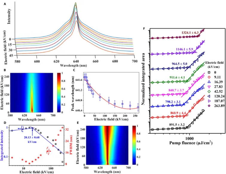
Electric field–dependent ASE
With increasing optical pump fluence across our device under zero electric field, a remarkable reduction in the FWHM and a sudden increase in the integrated intensity of the edge emission show a clear transition from spontaneous emission to ASE (see section S2). The ASE peak has a redshift of ~3.4 nm compared with the sponta-neous emission peak when the pump fluence increases from 270 to 1605 J/cm2 (fig. S7), as expected from biexcitonic gain in our CQDs. The ASE threshold is around 890 J/cm2, which is higher than the
pre-viously reported threshold (27) for CdSe/CdS/ZnS CQDs (~600 J/cm2, when pumped by a femtosecond pulse laser). Three effects here are possibly responsible for the increased ASE threshold: (i) The multiple layers can cause the pump fluence reduction because of the reflection and scattering at each layer and their interfaces; (ii) com-pared with the femtosecond laser, our 0.5-ns pulsed laser pump has to compete with very fast nonradiative Auger recombination to build up the population inversion; and (iii) the significant reduction of CQD absorption at our pumping wavelength (532 nm) when com-pared with that at the femtosecond pump wavelength (480 nm), as seen in Fig. 1A. Here, we explore the electric field–dependent ASE at a pump fluence of 1605 J/cm2, which can show the dominant
stimulated emission and will not cause thermal degradation of the device. The stimulated emission spectra as a function of the electric field are presented in Fig. 2A. The increasing electric field leads to a continuous enhancement in the stimulated emission intensity (Fig. 2B), which is predicted for charged CQDs (see the charge
injec-tion mechanism in fig. S5) as it is easier for them to achieve popula-tion inversion. Meanwhile, the ASE peaks exhibit a blueshift of ~1.2 nm (see Fig. 2C) when the electric field increases from 0 to 264 kV/cm. The blueshift in the spectrum, together with the intensity enhance-ment of ASE, indicates contradicting behaviors associated with the QCSE, implying the dominant charging effect in our CQD device. The blueshift in ASE implies lower reabsorption along the stripe waveguide due to the occupied state in the conduction band by extra electrons. However, the increase in ASE intensity is only true when the electric field is low. As the applied electric field exceeds a certain value, the behavior of stimulated emission goes to an opposite direction.
It is shown in Fig. 2D that, at the turning point of ~20.13 kV/cm, we observe a reversed knee behavior in the integrated ASE intensity versus the applied electric field. It is akin to the ASE’s pumping threshold extracted from the light input–light output curve (28); here, we name it as the “E-field threshold.” Below the E-field threshold, the FWHM of the stimulated emission is narrower, and the intensity of the stimulated emission is enhanced as the electric field increases (shown in Fig. 2, B, D, and E). Beyond the E-field threshold, the ASE intensity decreases exponentially as the electric field increases, as shown by the fit to the experimental data in Fig. 2D. At the electric field of 264 kV/cm, the FWHM increases to ~33.3 nm, which is close to that of the spontaneous emission (~35 nm) of the CQD films.
As shown in Fig. 2F, we have achieved an ~10% reduction in the ASE threshold by applying an electric field, which is far from the theoretical calculation: ~40% threshold reduction is expected for singly charged CQDs, and the zero threshold is predicted for doubly charged CQDs (6). However, it should be noted that the theoretical calculation for the threshold is only for the population inversion or the optical transparency of the materials, while the ASE threshold can be only achieved with the net gain where the optical gain dominates all the optical loss. One can probe the optical transparency of the material with the transient absorption experiment but might not achieve ASE because of the low gain coefficient and large optical loss (29). Never-theless, this behavior of first increasing and then decreasing threshold in our device with respect to the electric field implies multiple com-peting mechanisms. This leads us to delve into the electric field–induced spectroscopy in greater depth and figure out the dominant recom-bination processes with respect to different electric fields.
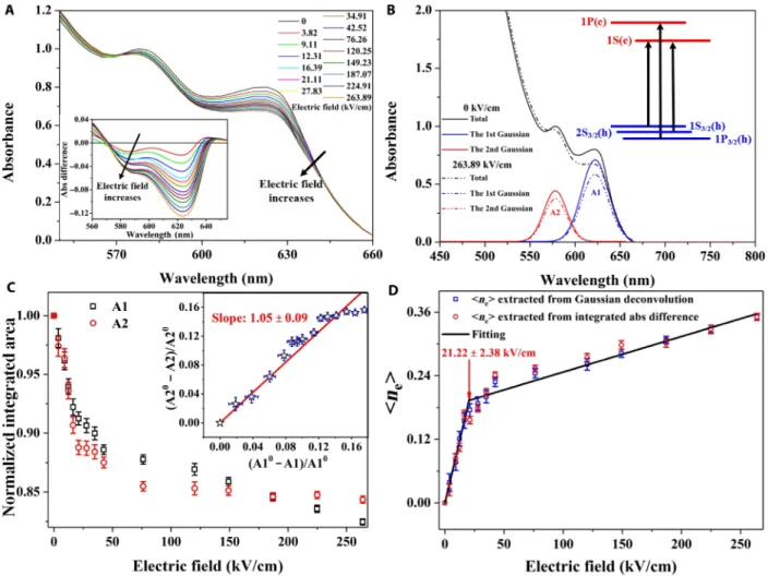
Competing mechanism in CQDs under varied electric fields
Quantifying the bleaching of the absorbance features can shed light on the occupied states in the conduction band of CQDs and give us more information about the ongoing transition processes. Here, we calculate the absorbance spectra from measuring electric field– dependent reflectance spectra of our device under different electric fields (see related equations, measurement setup, and data in section S3; figs. S8 to S10). As illustrated in Fig. 3A, the increase in the applied electric field results in progressive reduction in the ampli-tude of the first and second excitonic absorbance peaks. We also notice that the absorbance at the pumping wavelength (532 nm) is enhanced slightly as the electric field increases because of the reduced energy required for trion formation. However, at ~21 kV/cm, this enhancement (<0.3%) is negligible compared with the achieved threshold modulation (>10%) (see more details in section S3). To be quantitative about the degree of charging (the average excess electrons per CQD, <ne>), the absorbance spectra are fitted to the sum of four
Gaussian fittings (Fig. 3B and fig. S11) (20, 30, 31). According to the two lowest allowed interband transitions in CdSe/CdS/ZnS CQDs
(inset of Fig. 3B) (31), we can assign the first Gaussian peak (A1) to 1S(e)-1S3/2(h) transition and the second Gaussian peak (A2) to
1S(e)-2S3/2(h) transition.
Thus, <ne> can be estimated from the reduction of the integrated
area of each Gaussian fitting, providing that a 100% bleaching cor-responds to two excess electrons occupying the 1S(e) state in the conduction band (20, 32). A plot of the integrated area of A1 and A2 as a function of the applied electric field (Fig. 3C) indicates that bleaching of the 1S(e)-1S3/2(h) and 1S(e)-2S3/2(h) almost changes at
the same pace with the increase in electric field. Specifically, the decrease in the integrated area of A2 (−∆A2/A20) versus the decrease in the integrated area of A1(−∆A1/A10) can be well fitted by the line
with a slope of ~1.05 (inset of Fig. 3C). The result suggests that the 1S(e)-1S3/2(h) and 1S(e)-2S3/2(h) transitions have the same absorption
strength (30) and show the same degree of bleaching in the absorption
spectra when applying the electric field because the single- state 1S(e) is involved in both transitions. However, when the E-field is high (>200 kV/cm), the −∆A2/A20 increases slower than −∆A1/A10, imply-ing more absorption strength reduction for 1S(e)-1S3/2(h) than
1S(e)-2S3/2(h). Meanwhile, the integrated areas of the other two
Gaussian curves, A3 and A4 (fig. S12), remain virtually unchanged with respect to the applied electric field, implying that no excess electrons can be induced in the states beyond 1S(e) with the electric field up to 264 kV/cm.
We adopt two ways to calculate <ne>. One method is based on
extracting <ne> from the first Gaussian fitting of the absorbance
spectra. Another way is to calculate <ne> by integrating the
absorb-ance difference (inset of Fig. 3A). As shown in Fig. 3D, they are consistent with each other. Up to the electric field of 264 kV/cm, we find a maximum <ne> of ~0.35. According to the previous reports Fig. 2. Electric field–dependent ASE characteristics. (A) Emission spectra as a function of electric field with the pump fluence of 1605 J/cm2, indicating the “increases first and decreases later” trend of the emission intensity. (B) Two-dimensional (2D) spectra map normalized by the maximum peak ASE intensity. The maximum peak in-tensity occurred in an electric field of ~20 kV/cm. (C) Peak wavelength of ASE as a function of electric field. The stimulated emission peaks exhibit a blueshift of ~1.2 nm under the maximum electric field of 264 kV/cm. The solid line is a guide to the eye. (D) Integrated emission intensity (log-log plotting) and the FWHM of emission profile (semilog plotting) as a function of electric field. Turning point of the integrated emission intensity and the FWHM implies different dominant recombination processes as electric field increases. (E) 2D spectra map normalized by the peak ASE intensity at each electric field, showing spectrum width reduces first and increases afterward. (F) Light input–light output curves with increasing electric field. The straight lines are guides to the eyes. It shows clear evidence of controlling and tuning the ASE by electric field.
about photochemical charging (20), there is a linear correlation between <ne> and the amount of hole quenchers, while it is also true
for electrochemical charging where <ne> varies linearly with the
charges flowing into the CQDs (32). Here, the linear relationship between <ne> and applied electric field is still valid in our case. However,
<ne> increases at different rates in the low and high regimes of electric
field. A reasonable explanation for this observation is the different charging levels for a portion of CQDs in the thick film. Although <ne> is only 0.35, the charges are likely distributed to the CQDs at
the interfaces with other dielectric materials (SiO2 and PVP), while
the measured absorbance bleaching is the average effect of the ensemble CQDs. Hence, the turning point in the electric field of ~21 kV/cm is the indication that singly negatively charged CQDs are starting to become doubly negatively charged CQDs. Because of the Coulomb repulsion effect, it is more difficult for the electric field to in-duce one more electron to singly charged CQDs compared with the neutral ones. The electric field value of ~21 kV/cm matches the E-field
threshold that we discussed in Fig. 2, signifying that singly charged and doubly charged CQDs should be responsible for the E-field threshold behavior of the “first increasing and then decreasing” ASE intensity.
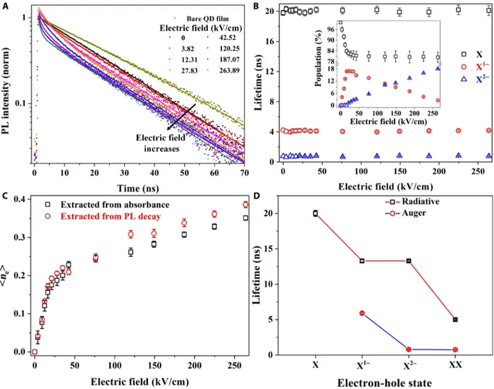
To further verify the validity of the electric field–induced charging process in CQDs, we analyze the effect of the applied electric field on PL dynamics. Different processes associated with different physical properties of CQDs can be distinguished via the time-resolved PL (trPL) analysis if their decay rates are different. The radiative lifetime value inferred from the trPL measurement can elucidate the question in Fig. 1 about the dominant factor causing the reduction of sponta-neous emission intensity: whether QCSE or charging effect dominates in CQDs. The two factors affect the spontaneous emission in different ways: QCSE weakens the radiative recombination (23), whereas trions can both accelerate nonradiative Auger recombination and en-hance the radiative process compared with the neutral exciton (8).
Figure 4A shows the PL decay of a CQD film measured under different electric fields. All the data are measured with the same Fig. 3. Quantification of the charging level in CQDs. (A) Visible absorbance spectra of CQDs under different electric fields. Inset: Absorbance spectra difference of
the first excitonic features, which is defined as the CQD absorbance under electric field subtracted by the CQD absorbance under no electric field. (B) An example of deconvolution of the absorbance spectrum into the sum of four Gaussian fittings. Inset: The lowest three allowed interband transitions of CQDs. (C) Normalized inte-grated area of A1 and A2 as a function of electric field, suggesting the electron occupation of the 1S(e) state of the conduction band. Inset: Relationship between the relative bleach of the first and the second transitions. The solid line with the slope of ~1.05 is the linear fitting of the data (A10, A20 denote A1 and A2 under no electric field, respectively). (D) Average electron number per CQD, <ne>, with respect to electric field. The red circles are <ne> extracted from the absorbance bleach of the 1S(e)-1S3/2(h) transition via Gaussian deconvolution. The blue squares are <ne> calculated from the integrated absorbance difference, which is normalized by the maximum <ne> obtained by Gaussian deconvolution. The solid line shows the linear fitting to the data. The turning point (21.22 kV/cm) is consistent with the E-field threshold (20.13 kV/cm) defined in Fig. 2.
collection time and then normalized by the maximum intensity of the CQD film without electric field. Hence, the results allow us to extract not only the decay rates but also the relative intensity among different electric fields at any decay time. Without the electric field, the single-exponential decay process for the CQD film (lifetime: ~20.1 ns) in the device structure is slightly faster than that for a bare CQD film on glass (lifetime: ~25 ns) because of the different dielec-tric environments (6, 8). We notice that the PL signal at early time increases relative to that in neutral CQDs. This phenomenon results from the enhanced radiative process in charged CQDs and supports the argument that charging effect, instead of QCSE, is responsible for the spectroscopy changes. However, time-integrated PL still shows the intensity reduction with the increasing electric field due to the Auger process caused by the extra electron. As the electric field in-creases, both enhanced radiative recombination and the Auger pro-cess are responsible for trPL becoming continuously faster.
To develop more insight, we fit each decay curve to extract the dynamics with different electric fields (solid lines in Fig. 4A). With
increasing electric fields, two new fast decay components appear. As illustrated in Fig. 4B, these two fast decay components (4.1 and 0.75 ns) are well correlated with the singly charged exciton lifetime (5 ns) and doubly charged exciton lifetime (2 ns) measured in single quasi– type II CQD for blinking study (33). Slightly faster decay in our sample compared with (33) is understandable as a single CQD nor-mally has a longer lifetime than a CQD ensemble, and our CQD film experiences different dielectric environments. To eliminate other possibilities (Auger process or carrier trapping), we have conducted fluence-dependent trPL to justify the lifetime assignment (details are presented in section S4; fig. S13). Hence, we can safely assign the lifetimes of 20.1, 4.1, and 0.75 ns to neutral exciton, singly charged exciton, and doubly charged exciton, respectively. It is important to note that these three lifetimes remain almost constant with increasing electric field, implying that electric field changes only the popula-tion of X0, X1−, and X2− and further confirming that a change of the
integrated wave function overlap caused by the electric field (QCSE) is very small in our case.
Fig. 4. Evolution of decay lifetime in CQDs with respect to the applied electric field. (A) trPL decays with increasing electric fields. Dots are the experimental results,
and solid lines are the fitting curves. The dark yellow decay curve is the result of bare CQD film on glass without electric field, while the black one is the decay of CQD film in the device structure without electric field. (B) Lifetimes as a function of the electric field extracted from the fitting of the decay curves with three exponential components. X, X1−, and X2− denote the neutral CQDs, singly charged CQDs, and doubly charged CQDs, respectively. Inset: Normalized population of X, X1−, and X2− as a function of the electric field. (C) Compare average charge per CQD, <ne>, extracted from absorption spectra and PL decays. The consistence here supports our previous explanations in Figs. 2 and 3. (D) Auger and radiative lifetimes of different electron-hole states. XX denotes the biexciton of neutral CQDs. The biexciton lifetime used here is cited from (33) for a similar CQD structure. In our device structure, Auger lifetime of the biexciton is quite close to Auger lifetime of the doubly charged trion (0.75 ns compared with 0.79 ns).
From the fitting parameters of trPL, we can derive populations of X0, X1−, and X2− (inset of Fig. 4B) with different electric fields.
With low electric field, only neutral-state and singly charged excitons contribute to the PL intensity dynamics. However, as electric field goes beyond a certain level (~21 kV/cm), the amount of X2− soars up, while the population of neutral CQDs remains unchanged. This trend largely agrees with the conclusion drawn from the steady-state absorbance analysis: Electric field can only charge a portion of the CQD populations. At the optimal electric field (~21 kV/cm), our device charges 17% of the CQD population to lower the threshold by ~10%.
We can perform a simple calculation to extract <ne> (<ne> = 0 ×
X0 + 1 × X1− + 2 × X2−) based on the derived populations. As shown
in Fig. 4C, <ne> extracted from the PL decay exhibits a good
agree-ment with that obtained from the optical bleaching. The maximum deviation of less than 0.04 electron per CQD is acceptable, consid-ering the Gaussian deconvolution and exponential fitting process. From the standpoint of optical gain applications, we are concerned more about the radiative recombination and the Auger process under different conditions. We assume that neutral exciton lifetime (20.1 ns) is purely radiative based on the fact that the PL of CQDs without electric field is a single exponential decay (almost a straight line in our semilog plotting). Hence, we can deduce the radiative lifetime of X1−,
X2−, and the neutral biexciton, XX, using the relationship radiative = 20.1/
( is the radiative enhancement factor). Statistically, is 4 for bi-excitons, while is 2 for singly and doubly charged exciton. However, recent reports (33) show that the electron repulsion effect occurring in charged CQDs will result in a factor less than 2. Here, we use = 1.5 according to the fitting results of PL dynamics using a Poisson dis-tribution model (see details in section S4; fig. S14) (6). Thus, we can calculate the Auger lifetime using the following equation: 1/total = 1/
radiative + 1/Auger. As shown in Fig. 4D, the Auger lifetime of X1− is about 5.9 ns, which is much lower than the Auger process (~730 ± 47 ps; see fig. S13) in the biexciton (34). However, the Auger lifetime of the doubly charged exciton (~790 ps) is quite close to the value in the neutral biexciton. The stimulated emission rate of X2− is twofold less than the stimulated emission rate (section S5) in the biexciton.
Modeling the electric field–dependent threshold
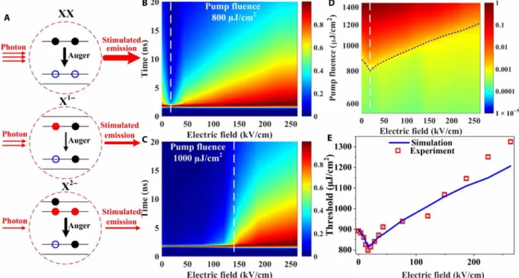
We have now quantified the lifetimes of X, XX, X1−, and X2− by fitting the PL dynamics. Meanwhile, we know the population of each state as a function of the applied electric field obtained by analyzing the trPL and absorbance bleaching data. Therefore, we can apply the rate equations to evaluate the ASE threshold with different electric fields. The model we use here is based on the recent calculations for optical gain, which considers both the Auger process and optical cavity losses (35–37). We adopt the rate equations for neutral and singly/doubly charged CQDs and plug in the electric field–dependent population distribution and all the recombination rates to complete our model [see the detailed parameters, transition processes (fig. S15), rate equations, and simulated dynamics (figs. S19 and S20) in section S5]. Figure 5A shows a cartoon of the stimulated emission process in neutral, singly, and doubly charged CQDs, respectively. In neu-tral CQDs, a biexciton is required for population inversion, which is harder to achieve but provides better gain coefficient. Singly charged CQDs lower the requirement for population inversion due to the preexisting electron in the conduction band. For X2−, the doubly
charged CQDs are transparent and achieve population inversion with any excitation level. However, the enhanced Auger recombination (compared with singly charged CQDs) and less efficient radiative
recombination (compared with biexcitons) deplete the exciton very fast. This affects the optical gain in two ways: fewer emission photons to trigger stimulated emission and fewer excitons to contribute to stimulated emission. One can experimentally show negative absorp-tion (populaabsorp-tion inversion) in transient absorpabsorp-tion measurement at very low pumping level, but the demonstration of ASE where the gain has to overcome various losses is very challenging (29). In addition, obtaining the net gain out of the doubly charged CQDs is more difficult with our subnanosecond pumping source because of the very short gain lifetime, governed by dominant nonradiative Auger recombination.
Here, we simulate the dynamics of emitted photon density as a function of the applied electric field under different pump fluence. As presented in section S5, we only consider the photons coupling to the waveguide and participating in the ASE process. Noncoupling photons (~95.5%; see the COMSOL simulation in fig. S16) are spontaneously emitted out of the CQD film. At the pump fluence of 800 J/cm2 (Fig. 5B and fig. S18A), the abrupt acceleration of photon
emission, which is the evidence of the onset of ASE, can only be achieved with the electric field around 21 kV/cm. When the electric field is too low or too high, there is only spontaneous emission. It is consistent with the E-field threshold of ~20 kV/cm extracted from the electric field–dependent ASE characterization (Fig. 2), implying that singly charged CQDs help build up the net gain in our device. In the case of high pump fluence, 1000 J/cm2 (Fig. 5C and fig. S18B), the ASE can happen with the electric field up to ~149 kV/cm. This behavior illustrates the stimulated emission process presented in Fig. 5A: Optimum electric field creates enough singly charged CQDs and enables ASE at lower threshold, while higher electric field increases the population of doubly charged CQDs and results in higher threshold for optical net gain (ASE). Our model also suggests that if a device can charge the entire CQD population with a single electron, then we would be able to lower the ASE threshold down to ~35% compared with neutral CQDs, which is slightly less than the theoretical improvement (~40%) for the population inversion threshold (6) due to finite loss in ASE.
The time integration of the emitted photon density (log scale) as a function of the applied electric field (linear scale) and pump fluence (log scale) is shown in Fig. 5D. The threshold with different electric fields (dashed blue line in Fig. 5D and fig. S17) is extracted as the transition point from spontaneous emission to stimulated emission. In Fig. 5E, we compare the simulated ASE threshold trend with the experimental results. With low electric field, the simulated result is in very good agreement with the “up and down” threshold behavior (Fig. 2) up to the electric field of ~200 kV/cm. At higher electric field, the simulation shows lower threshold than the experiment data. This is understandable as our model considered only up to doubly charged CQDs, which would only be valid at low electric field. The Auger re-combination rate will increase faster with more electrons in CQDs, and therefore, achieving the optical net gain is harder in the experiment.
CONCLUSION
In summary, we have demonstrated controllable and tunable ASE in a colloidal semiconductor device via electric field–induced charging. The contribution of neutral, singly, and doubly charged CQDs to the ASE are quantitatively determined by analyzing the competing mechanisms happening in the CQD population. Neutral CQDs need high optical pump to create biexcitons, compete with fast
nonradiative Auger recombination, and achieve high optical gain. Singly charged CQDs can lower the optical gain threshold because of the partially filled conduction band and low Auger recombination rate. Doubly charged CQDs can, in principle, achieve population inversion with any pumping level, but achieving the net gain still requires a significantly high pumping level due to enhanced nonradia-tive Auger recombination and low gain coefficient. Our kinetics model to simulate the ASE behavior shows very good consistence with the experimental results, highlighting the dominant role of singly charged CQDs to achieve low ASE threshold. Our work demonstrates the feasibility of controlling not only exciton recom-bination dynamics but also the CQD charging level to lower the threshold of CQD lasing in a device structure. Our results suggest that good control of the charging process for the entire CQD film will significantly improve the CQD lasers and lower the threshold to pos-sibly enable continuous wave or electrically driven devices.
MATERIALS AND METHODS Synthesis of CdSe/CdS/ZnS CQDs
Here, the recipe is a slightly modified facile one-pot method (1, 27, 38). Amounts of 1 mmol of cadmium oxide (CdO; >99.99%), 18.85 mmol of oleic acid (OA; 90%), and 2 mmol of zinc acetate [Zn(AC)2; 99.99%]
were mixed with 25 ml of 1-octadecene (1-ODE; 90%) in a three-neck flask. The mixture was evacuated for 15 min and heated to 300°C
under nitrogen condition. After that, selenium precursor made by dissolving 0.2 mmol of selenium power (Se; >99.99%) in 0.2 mmol of trioctylphosphine (TOP; 90%) was quickly added into the reaction flask at 300°C. Three minutes later, 0.3 ml of dodecanethiol (DT; >98%) was injected slowly into the mixture. The reaction lasts for 20 min to get CdSe/CdS QDs. Subsequently, sulfur precursor made by dis-solving 2 mmol of sulfur powder (S; >99.5%) in 1 mmol of TOP was added to react with the excess Cd ions and passivate the surface with ZnS shell. CdSe/CdS/ZnS (core-shell-shell) CQDs were purified with ethanol several times and dispersed in toluene for film fabrication.
Characterization of CdSe/CdS/ZnS CQDs
Absorption spectra of CQDs in toluene (1 mg/ml) were measured using an ultraviolet-visible spectrophotometer (Shimadzu, UV-1800). PL spectra of CQDs in toluene (1 mg/ml) were recorded using a spectrofluorophotometer (Shimadzu, RF-5301PC; excitation wavelength, 532 nm). QY of CQDs in toluene (100 mg/ml) was measured with an integrating sphere and calculated as the ratio of absolute emission pho-tons and absorption phopho-tons. The accuracy of the QY measurement was verified using Rhodamine 6G, and the measured QY of 94.3% in our setup was in good agreement with the standard value of 95%.
Device fabrication
First, the glass substrate with ITO was patterned to yield three devices per substrate; the top 2 devices were with CQD film, which Fig. 5. Modeling of the ASE threshold using the kinetic equations and experimental parameter inputs. (A) Schematics of the ASE process in neutral and charged CQDs. Blue
hollow circles represent holes in the valence band. Black solid circles represent photogenerated electrons, while red solid circles denote excess electrons induced by the electric field. XX, X1−, and X2− are the same denotations as previously described in Fig. 4. (B and C) Emission intensity decay map normalized by the peak value of the photon density under each electric field at the pump fluence of 800 and 1000 J/cm2, respectively. At 800 J/cm2, the abrupt acceleration of emission (ASE) only occurs under the E-field threshold (20.13 kV/cm). The white dash line locates at the E-field threshold. At 1000 J/cm2, the ASE can be observed under the electric field smaller than 149.2 kV/cm (white dash line). (D) Integrated photon density (log scale) map as a function of both the applied electric field (linear scale) and the pump fluence (log scale). The white dash line indicates the E-field threshold, and the blue dash line indicates the threshold behavior under different electric fields. (E) Simulated and experimental ASE threshold behavior as a function of the applied electric field.
provided redundancy in the fabrication process for testing repro-ducibility, while the bottom one was exactly the same structure but without CQD film, which was used as a reference for steady-state absorption measurement (see details in section S3). After that, glass substrates were carefully cleaned and ultrasonicated. Then, an SiO2
layer with a thickness of ~160 nm was deposited via sputtering (UNIVEX 350; radio frequency, 150 W). The CQD film was deposited by the spin-casting technique (spin duration, 3 min; spin velocity, 500 rpm/s). Another dielectric layer was a PVP film deposited on top of the CQD film also by spin casting [PVP dissolved in etha-nol (20 mg/ml); spin duration, 45 s; spin velocity, 2000 rpm/s]. All the spin-casting processes were made inside the glove box, and each spin- casting step was followed by baking the device at 60°C in a nitrogen environment for 20 min. Last, the sample was loaded into a thermal evaporator to deposit the aluminum layer as the top electrode.
Capacitance of the dielectric layers
The capacitance of each dielectric layer was determined using the equation of parallel plate capacitor: C = A × /d, where A is the area of the capacitor (8 mm × 2 mm), d is the thickness of each layer determined by the scanning electron microscopy measurement and surface profiler measurement (DektakXT surface profiler), and is the permittivity of each dielectric film. Here, low-frequency permit-tivity was approximated as that at optical frequency and measured using an ellipsometer (VASE, J.A. Woollam; spectral range from 193 to 3200 nm). The measurement data and fitting process of the permittivity can be found in section S1 (fig. S3). The voltage drop across the CQD layer was calibrated via the calculation of the charge stored in insulator layers (see details in fig. S4).
AC bias and stripe excitation
The sinusoidal AC bias was generalized by the function generator (FG500A, WAVETEK) with a frequency of 128 Hz, and the pump laser at 532 nm used for stripe excitation was a frequency-doubling Nd:YAG laser with a pulse width of 0.5 ns and a repetition rate of 100 Hz. The laser beam was focused onto a stripe along the device structure using a cylindrical lens and incidents from the glass sub-strate. The width of the stripe, which contains (1 − 1/e) of the power in the laser beam, was 50 m, determined using the knife-edge method. In the experiment, the stripe length was 4 mm. An auto-matically rotated /4 wave plate (WPQ05M-532, Thorlabs) and polarizer (CCM1-WPBS254, Thorlabs) were used to adjust the pump fluence on device. Then, the emission was collected via a fiber-coupled Andor spectrometer (monochromator: Andor Shamrock 303i; charge- coupled device: Andor iDus 401). The collection geometry was per-pendicular to the laser pump. All measurements were performed at room temperature in air.
Steady-state absorption measurement
The white light generated by the light source (ELS-250, Asahi Spectra) was filtered by a monochromator (7ISWS; spectral selection range, 330 to 1000 nm) and then focused onto the device through the glass substrate at an angle of 45°; a silicon detector (Newport 2031; 400 to 1070 nm) was used to collect the reflection light off the device. Light transmitted through the CQD layer twice when reflecting off the device. The silicon detector was connected to a lock-in amplifier (SR830, Stanford Research System). The measurement setup and calculation details are shown in section S3.
PL dynamics measurement
The trPL spectroscopy was performed in a confocal system with Micro Photon Devices single-photon avalanche photodiode and a time- correlated single-photon counting acquisition module (Edinburgh Instruments, TCC900). For the excitation, we used a pulsed diode laser at 355 nm with a repetition rate of 10 MHz, while we filtered the emission at 640 ± 20 nm. For all the trPL measurements using the diode laser, the temporal resolution was 200 ps. For the femto-second laser PL lifetime measurements, the output from a 1-kHz, 50-fs Coherent Libra Regenerative Amplifier (800 nm) that was frequency doubled using a beta-barium borate crystal (to 400 nm) was used as the pump source. The emission from the samples was detected by an Optronis Optoscope streak camera system, which has an ultimate temporal resolution of 10 ps.
SUPPLEMENTARY MATERIALS
Supplementary material for this article is available at http://advances.sciencemag.org/cgi/ content/full/5/10/eaav3140/DC1
Section S1. Electric field and current in the CQD device Section S2. ASE in the CQD device without electric field Section S3. Steady-state absorption measurement Section S4. PL dynamics analysis
Section S5. Kinetics model Fig. S1. Schematics of the circuit.
Fig. S2. Thickness measurement conducted by surface profiler (DektakXT surface profiler). Fig. S3. Permittivity measurement result.
Fig. S4. Mutual corroboration to calibrate the voltage drop. Fig. S5. Energy schematic of the device.
Fig. S6. Measured current flowing through the circuit.
Fig. S7. Edge emission as a function of pump fluence without electric field under 500-ps laser pulse excitation (532 nm).
Fig. S8. Measurement setup for electric field–dependent absorbance. Fig. S9. Measuring the transmittance of the CQD layer.
Fig. S10. Steady-state absorbance measurement.
Fig. S11. Gaussian fitting (red dashed line) of absorbance spectra (black solid line). Fig. S12. Integrated area of A3 as a function of electric field.
Fig. S13. Fluence-dependent lifetime probe at peak wavelength.
Fig. S14. Fitting results of the subtraction of PL dynamics at different electric fields. Fig. S15. Optical transition processes in neutral CQDs (X), singly charged CQDs (X1−), and doubly charged CQDs (X2−).
Fig. S16. COMSOL simulation to determine the coupling efficiency. Fig. S17. Photon emission density as a function of pumping intensity.
Fig. S18. The 2d emitted photon decay map under each electric field at the pump fluence of 800 J/cm2 and 1000 J/cm2.
Fig. S19. Population dynamics under an electric field of ~21 kV/cm and with a pump fluence of 100 J/cm2.
Fig. S20. Population dynamics under an electric field of ~21 kV/cm and with a pump fluence of 1000 J/cm2.
References (39–45)
REFERENCES AND NOTES
1. O. Chen, J. Zhao, V. P. Chauhan, J. Cui, C. Wong, D. K. Harris, H. Wei, H.-S. Han, D. Fukumura, R. K. Jain, M. G. Bawendi, Compact high-quality CdSe–CdS core–shell nanocrystals with narrow emission linewidths and suppressed blinking. Nat. Mater. 12, 445–451 (2013). 2. L. E. Brus, Electron–electron and electron-hole interactions in small semiconductor
crystallites: The size dependence of the lowest excited electronic state. J. Chem. Phys. 80, 4403–4409 (1984).
3. C. B. Murray, D. J. Norris, M. G. Bawendi, Synthesis and characterization of nearly monodisperse CdE (E = sulfur, selenium, tellurium) semiconductor nanocrystallites.
J. Am. Chem. Soc. 115, 8706–8715 (1993).
4. C. Dang, J. Lee, C. Breen, J. S. Steckel, S. Coe-Sullivan, A. Nurmikko, Red, green and blue lasing enabled by single-exciton gain in colloidal quantum dot films. Nat. Nanotechnol. 7, 335–339 (2012).
5. F. Fan, O. Voznyy, R. P. Sabatini, K. T. Bicanic, M. M. Adachi, J. R. McBride, K. R. Reid, Y.-S. Park, X. Li, A. Jain, R. Quintero-Bermudez, M. Saravanapavanantham, M. Liu, M. Korkusinski, P. Hawrylak, V. I. Klimov, S. J. Rosenthal, S. Hoogland, E. H. Sargent, Continuous-wave lasing in colloidal quantum dot solids enabled by facet-selective epitaxy.
6. K. Wu, Y.-S. Park, J. Lim, V. I. Klimov, Towards zero-threshold optical gain using charged semiconductor quantum dots. Nat. Nanotechnol. 12, 1140–1147 (2017).
7. V. I. Klimov, A. A. Mikhailovsky, S. Xu, A. Malko, J. A. Hollingsworth, C. A. Leatherdale, H.-J. Eisler, M. G. Bawendi, Optical gain and stimulated emission in nanocrystal quantum dots.
Science 290, 314–317 (2000).
8. B. Patton, W. W. Langbein, U. Woggon, Trion, biexciton, and exciton dynamics in single self-assembled CdSe quantum dots. Phys. Rev. B 68, 125316 (2003).
9. V. I. Klimov, Multicarrier interactions in semiconductor nanocrystals in relation to the phenomena of Auger recombination and carrier multiplication.
Annu. Rev. Condens. Matter Phys. 5, 285–316 (2014).
10. B. Guilhabert, C. Foucher, A.-M. Haughey, E. Mutlugun, Y. Gao, J. Herrnsdorf, H. D. Sun, H. V. Demir, M. D. Dawson, N. Laurand, Nanosecond colloidal quantum dot lasers for sensing. Opt. Express 22, 7308–7319 (2014).
11. L. J. McLellan, B. Guilhabert, N. Laurand, M. D. Dawson, CdSxSe1-x/ZnS semiconductor nanocrystal laser with sub 10kW/cm2 threshold and 40nJ emission output at 600 nm.
Opt. Express 24, A146–A153 (2016).
12. C. E. Rowland, K. Susumu, M. H. Stewart, E. Oh, A. J. Mäkinen, T. J. O’Shaughnessy, G. Kushto, M. A. Wolak, J. S. Erickson, A. L. Efros, A. L. Huston, J. B. Delehanty, Electric field modulation of semiconductor quantum dot photoluminescence: Insights into the design of robust voltage-sensitive cellular imaging probes. Nano Lett. 15, 6848–6854 (2015).
13. C. Wang, B. L. Wehrenberg, C. Y. Woo, P. Guyot-Sionnest, Light emission and amplification in charged CdSe quantum dots. J. Phys. Chem. B. 108, 9027–9031 (2004).
14. F. De Martini, G. R. Jacobovitz, Anomalous spontaneous–stimulated-decay phase transition and zero-threshold laser action in a microscopic cavity. Phys. Rev. Lett. 60, 1711–1714 (1988). 15. B. Ellis, M. A. Mayer, G. Shambat, T. Sarmiento, J. Harris, E. E. Haller, J. Vučković,
Ultralow-threshold electrically pumped quantum-dot photonic-crystal nanocavity laser.
Nat. Photonics 5, 297–300 (2011).
16. S. Chen, W. Li, J. Wu, Q. Jiang, M. Tang, S. Shutts, S. N. Elliott, A. Sobiesierski, A. J. Seeds, I. Ross, P. M. Smowton, H. Liu, Electrically pumped continuous-wave III–V quantum dot lasers on silicon. Nat. Photonics 10, 307–311 (2016).
17. A. M. Dennis, B. D. Mangum, A. Piryatinski, Y.-S. Park, D. C. Hannah, J. L. Casson, D. J. Williams, R. D. Schaller, H. Htoon, J. A. Hollingsworth, Suppressed blinking and Auger recombination in near-infrared type-II InP/CdS nanocrystal quantum dots. Nano Lett. 12, 5545–5551 (2012).
18. Y.-S. Park, W. K. Bae, L. A. Padilha, J. M. Pietryga, V. I. Klimov, Effect of the core/shell interface on Auger recombination evaluated by single-quantum-dot spectroscopy.
Nano Lett. 14, 396–402 (2014).
19. F. García-Santamaría, Y. Chen, J. Vela, R. D. Schaller, J. A. Hollingsworth, V. I. Klimov, Suppressed Auger recombination in “giant” nanocrystals boosts optical gain performance. Nano Lett. 9, 3482–3488 (2009).
20. J. D. Rinehart, A. M. Schimpf, A. L. Weaver, A. W. Cohn, D. R. Gamelin, Photochemical electronic doping of colloidal CdSe nanocrystals. J. Am. Chem. Soc. 135, 18782–18785 (2013).
21. R. Scott, A. W. Achtstein, A. V. Prudnikau, A. Antanovich, L. D. A. Siebbeles, M. Artemyev, U. Woggon, Time-resolved stark spectroscopy in CdSe nanoplatelets: Exciton binding energy, polarizability, and field-dependent radiative rates. Nano Lett. 16, 6576–6583 (2016). 22. C. A. Leatherdale, C. R. Kagan, N. Y. Morgan, S. A. Empedocles, M. A. Kastner, M. G. Bawendi,
Photoconductivity in CdSe quantum dot solids. Phys. Rev. B 62, 2669–2680 (2000). 23. S. A. Empedocles, M. G. Bawendi, Quantum-confined stark effect in single CdSe
nanocrystallite quantum dots. Science 278, 2114–2117 (1997).
24. K. Park, Z. Deutsch, J. J. Li, D. Oron, S. Weiss, Single molecule quantum-confined stark effect measurements of semiconductor nanoparticles at room temperature. ACS Nano 6, 10013–10023 (2012).
25. S.-J. Park, S. Link, W. L. Miller, A. Gesquiere, P. F. Barbara, Effect of electric field on the photoluminescence intensity of single CdSe nanocrystals. Chem. Physics 341, 169–174 (2007). 26. A. I. Ekinov, A. L. Efros, T. V. Shubina, A. P. Skvortsov, Quantum-size stark effect in
semiconductor microcrystals. JOL 46, 97–100 (1990).
27. Y. Wang, V. D. Ta, Y. Gao, T. C. He, R. Chen, E. Mutlugun, H. V. Demir, H. D. Sun, Stimulated emission and lasing from CdSe/CdS/ZnS core-multi-shell quantum dots by simultaneous three-photon absorption. Adv. Mater. 26, 2954–2961 (2014). 28. D. Saxena, S. Mokkapati, P. Parkinson, N. Jiang, Q. Gao, H. H. Tan, C. Jagadish, Optically
pumped room-temperature GaAs nanowire lasers. Nat. Photonics 7, 963–968 (2013). 29. Q. Li, Z. Xu, J. R. McBride, T. Lian, Low threshold multiexciton optical gain in colloidal CdSe/
CdTe Core/Crown type-II nanoplatelet heterostructures. ACS Nano 11, 2545–2553 (2017). 30. W.-k. Koh, A. Y. Koposov, J. T. Stewart, B. N. Pal, I. Robel, J. M. Pietryga, V. I. Klimov,
Heavily doped n-type PbSe and PbS nanocrystals using ground-state charge transfer from cobaltocene. Sci. Rep. 3, 2004 (2013).
31. V. I. Klimov, Spectral and dynamical properties of multiexcitons in semiconductor nanocrystals. Annu. Rev. Phys. Chem. 58, 635–673 (2007).
32. M. Shim, C. Wang, P. Guyot-Sionnest, Charge-tunable optical properties in colloidal semiconductor nanocrystals. J. Phys. Chem. B. 105, 2369–2373 (2001).
33. C. Galland, Y. Ghosh, A. Steinbrück, M. Sykora, J. A. Hollingsworth, V. I. Klimov, H. Htoon, Two types of luminescence blinking revealed by spectroelectrochemistry of single quantum dots. Nature 479, 203–207 (2011).
34. M. M. Adachi, F. Fan, D. P. Sellan, S. Hoogland, O. Voznyy, A. J. Houtepen, K. D. Parrish, P. Kanjanaboos, J. A. Malen, E. H. Sargent, Microsecond-sustained lasing from colloidal quantum dot solids. Nat. Commun. 6, 8694 (2015).
35. Y.-S. Park, W. K. Bae, T. Baker, J. Lim, V. I. Klimov, Effect of auger recombination on lasing in heterostructured quantum dots with engineered core/shell interfaces. Nano Lett. 15, 7319–7328 (2015).
36. R. R. Cooney, S. L. Sewall, D. M. Sagar, P. Kambhampati, Gain control in semiconductor quantum dots via state-resolved optical pumping. Phys. Rev. Lett. 102, 127404 (2009).
37. S. L. Sewall, R. R. Cooney, K. E. H. Anderson, E. A. Dias, P. Kambhampati, State-to-state exciton dynamics in semiconductor quantum dots. Phys. Rev. B 74, 235328 (2006). 38. Y.-S. Park, W. K. Bae, J. M. Pietryga, V. I. Klimov, Auger recombination of biexcitons
and negative and positive trions in individual quantum dots. ACS Nano 8, 7288–7296 (2014).
39. S. Shendre, V. K. Sharma, C. Dang, H. V. Demir, Exciton dynamics in colloidal quantum-dot LEDs under active device operations. ACS Photonics 5, 480–486 (2018).
40. A. S. Kavasoglu, C. Tozlu, O. Pakma, N. Kavasoglu, S. Ozden, B. Metin, O. Birgi, S. Oktik, Investigation of temperature dependent dc current transport mechanism on Au/ poly(4-vinyl phenol)/p-Si device. J. Phys. D Appl. Phys. 42, 145111 (2009).
41. D. A. Hines, R. P. Forrest, S. A. Corcelli, P. V. Kamat, Predicting the rate constant of electron tunneling reactions at the CdSe–TiO2 interface. J. Phys. Chem. B 119, 7439–7446 (2015). 42. J. Huang, D. Stockwell, Z. Huang, D. L. Mohler, T. Lian, Photoinduced ultrafast electron
transfer from CdSe quantum dots to Re-bipyridyl complexes. J. Am. Chem. Soc. 130, 5632–5633 (2008).
43. B. Guzelturk, Y. Kelestemur, K. Gungor, A. Yeltik, M. Z. Akgul, Y. Wang, R. Chen, C. Dang, H. Sun, H. V. Demir, Stable and low-threshold optical gain in CdSe/CdS quantum dots: An all-colloidal frequency up-converted laser. Adv. Mater. 27, 2741–2746 (2015). 44. F. T. Rabouw, M. Kamp, R. J. A. van Dijk-Moes, D. R. Gamelin, A. F. Koenderink, A. Meijerink,
D. Vanmaekelbergh, Delayed exciton emission and its relation to blinking in CdSe quantum dots. Nano Lett. 15, 7718–7725 (2015).
45. R. Scott, J. Heckmann, A. V. Prudnikau, A. Antanovich, A. Mikhailov, N. Owschimikow, M. Artemyev, J. I. Climente, U. Woggon, N. B. Grosse, A. W. Achtstein, Directed emission of CdSe nanoplatelets originating from strongly anisotropic electronic structure.
Nat. Nanotechnol. 12, 1155–1160 (2017).
Acknowledgments
Funding: We would like to acknowledge the financial support from the Singapore Ministry of
Education AcRF Tier-1 grant (MOE-2017-T1-002-142). We are also grateful to acknowledge the financial support from the Singapore National Research Foundation under the program NRF-NRFI2016-08; the Competitive Research Program NRF-CRP14-2014-03; and the Singapore Agency for Science, Technology and Research (A*STAR) SERC Pharos Program under grant no. 152 73 00025. Author contributions: C.D. initiated the idea and led, supervised, and contributed to all aspects of the research. H.V.D. initiated and supervised the CQD synthesis and capacitor device fabrication. J.Y., H.V.D., and C.D. wrote the manuscript. J.Y., S.S., and B.L. fabricated the device. J.Y. performed the ASE measurements and the steady-state absorbance measurement. J.Y., S.H., and M.D.B. performed the PL dynamics measurement. M.L. conducted the fluence-dependent lifetime measurement. J.Y. and C.D. conducted the kinetic model simulation. S.S. and S.D. synthesized the CdSe/CdS/ZnS CQDs. P.H.-M. conducted the COMSOL simulation. C.H., W.-k.K., and J.Y. performed the SEM and TEM measurements. T.C.S. and H.W. discussed the results and provided the technical advice. All authors discussed the results, commented on the manuscript, and participated in the manuscript revision. Competing
interests: The authors declare that they have no competing interests. Data and materials availability: All data needed to evaluate the conclusions in the paper are present in the paper
and/or the Supplementary Materials. Additional data related to this paper may be requested from the authors.
Submitted 5 September 2018 Accepted 14 September 2019 Published 25 October 2019 10.1126/sciadv.aav3140
Citation: J. Yu, S. Shendre, W.-k. Koh, B. Liu, M. Li, S. Hou, C. Hettiarachchi, S. Delikanli, P. Hernández-Martínez, M. D. Birowosuto, H. Wang, T. Sum, H. V. Demir, C. Dang, Electrically control amplified spontaneous emission in colloidal quantum dots. Sci. Adv. 5, eaav3140 (2019).
Cuong Dang
DOI: 10.1126/sciadv.aav3140 (10), eaav3140.
5
Sci Adv
ARTICLE TOOLS http://advances.sciencemag.org/content/5/10/eaav3140
MATERIALS
SUPPLEMENTARY http://advances.sciencemag.org/content/suppl/2019/10/21/5.10.eaav3140.DC1
REFERENCES
http://advances.sciencemag.org/content/5/10/eaav3140#BIBL
This article cites 45 articles, 2 of which you can access for free
PERMISSIONS http://www.sciencemag.org/help/reprints-and-permissions
Terms of Service
Use of this article is subject to the
is a registered trademark of AAAS.
Science Advances
York Avenue NW, Washington, DC 20005. The title
(ISSN 2375-2548) is published by the American Association for the Advancement of Science, 1200 New
Science Advances
License 4.0 (CC BY-NC).
Science. No claim to original U.S. Government Works. Distributed under a Creative Commons Attribution NonCommercial Copyright © 2019 The Authors, some rights reserved; exclusive licensee American Association for the Advancement of