c
T ¨UB˙ITAK
Electron Spectroscopy for Material Characterization
S¸efik S ¨UZER
Bilkent University, Chemistry Department, 06533 Ankara-TURKEY
Received 04.05.1998
Basic principles of the two electron spectroscopic techniques, the x-ray photoelectron spectroscopy, XPS, and the Auger electron spectroscopy, AES, are given. Their utilization in material characterization are introduced through examples with application of these techniques to various surface related problems.
Introduction
The techniques utilizing the detection of emitted electrons as a result of exposure to energetic photons (X-ray Photoelectron Spectroscopy,XPS) or electrons (Auger Electron Spectroscopy, AES) have emerged as versatile tools for material characterization especially in surface related areas1−5. In both XPS and AES
all atoms except for H and He can be analyzed and the information derived stems from the atoms in the top 1-10 nm layers of the materials under investigation. The analysis depth can also be extended to about 103-104 nm, however, only by incorporation of additional etching techniques. Sputtering or ion-milling with energetic (1-5 keV) noble gas ions (like Ar+) are the most popular methods for depth-profiling6. After their
introduction in late 1960s by Kai Siegbahn in Uppsala, both XPS and AES have revolutionized concepts in many fields of chemistry, physics and material sciences. Unfortunately, only in 1994 the first instrument, capable of doing both XPS and X-ray induced AES analyses, was set-up in Turkey in our laboratory. In this article, we give examples of utilization of this technique for different kinds of surface-related problems carried out in our laboratory.
Basic Theory and Experimental Requirements
In XPS the sample is subjected to energetic photons (x-rays, with energy h ν and the energy of the primary electrons (K.E.) produced as a result of photoemission process are analyzed. The sought-out information, the binding energy (B.E.) is obtained through the energy conservation equation: h ν (known) = K.E. (measured) + B.E. The electrons appear as peaks having certain quantized energies and are designated according to the levels they are ejected from and they are designated as such i.e. F1s, Ca2p or Pb4f etc. The peaks for levels other than s are further split due to the spin-orbit coupling into doublets (p3/2-p1/2 or d5/2-d3/2 etc.).
Three parameters give important information; (i) the value of the B.E. ,
(iii) the angular dependency of the intensity I( Θ).
In AES the energy (K.E.) of the secondary electrons which are formed during the filling up of the initial core holes created by either the photoionization and/or electron-impact ionization are analyzed. The energy of these so-called Auger electrons are independent of the way in which the initial core-holes are created and are characteristic of the atoms present in the sample. The Auger electrons are designated by three letters indicative of (i) the level of the initial hole, (ii) the level from which the electron drops to fill the hole, and (iii) the level which the electron is ejected from. Hence NaKLL refers to the process where the
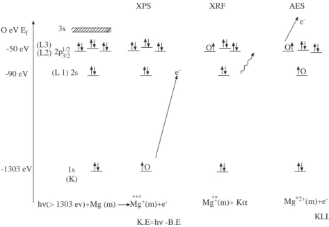
initial K hole (1s level) is filled by and electron from the L (2s or 2p) level and another L electron is ejected. The energy levels of a typical atom (magnesium) and the XPS, AES and the related process through which x-rays are created, XRF, are depicted in Figure 1. Accordingly, in the XPS spectrum of Mg in addition to the valence band (0-10 eV), a Mg2p spin-orbit doublet at around 50, a Mg2s peak at 90 and a Mg1s peak at around 1300 eV binding energies should be detected. Auger peaks having kinetic energies around 1100-1200 eV corresponding to KLL transitions should also be observed. In the XRF process, however, an energetic photon not an electron is produced.
O eV Ef -50 eV -90 eV 3s (L3) (L2) 2p1/23/2 (L 1) 2s XPS e -XRF AES O O e -O O 1s (K) hν(> 1303 ev)+Mg (m) Mg+(m)+e -*** Mg**+(m)+ Kα Mg*2+(m)+e -KLL -1303 eV K.E=hν -B.E
Figure 1. A schematic of the energy levels of Mg, the XPS, AES and XRF processes
Since it is the electrons which are analyzed and to avoid scattering of them by the residual gas molecules and also to enhance the surface sensitivity both techniques are performed under ultra-high-vacuum (UHV) conditions which require pressures better than 10−9 torr. In principle any solid sample in the form of a film or a pressed powder can be analyzed without any chemical/physical pretreatment (unlike electron microscopic techniques).
The electrons are also severely scattered by the solid environment where they are created and only the ones created at or near the surface can survive without inelastic energy losses. This very property is what makes these techniques surface sensitive. The escape depth of the electrons which is defined as three times the attenuation length (λ ) of the electrons within a given material which depends on the material as well as the energy of the electrons but vary typically between 1-10 nm for electrons having energies between 102-103 eV and for most inorganic and organic materials7.
Our instrument consists of a Kratos ES300 electron spectrometer with Al/Mg dual anode. The samples, in the form of films or pressed powders, are introduced directly from atmospheric pressure by a fast-lock entry compartment and the base pressure is kept below 2x10⁻⁹ torr during analysis by combination of diffusion and ion-pumps. A 1-3 keV Ar+ ion-gun is used for depth profiling or brief cleaning of the surface of the samples.
Qualitative Information
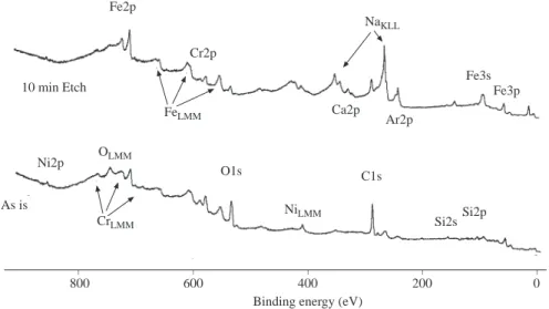
Figure 2 shows a typical electron spectrum of a stainless steel sample as introduced into the spectrometer (bottom part) and after brief surface cleaning with argon ions (top part) using unmonochromatized MgKα x-radiation (h ν =1253.6 eV). Spectra consists of features in the form of peaks at various binding (in actuality it is the kinetic energy which is measured energies which can be identified and assigned as shown in Table 1. As is evident O and C are also present in ample quantities on the surface of the material but can be removed by Ar+ion etching. Fe, Cr and Ni are the main constituents but other elements like Na, Ca and Si are also
present in this particular stainless steel sample.
Stainless Steel Fe2p Cr2p Fe3s Fe3p C1s Si2p Si2s O1s Ni2p Ca2p Ar2p FeLMM NiLMM CrLMM OLMM NaKLL As is 10 min Etch
Binding energy (eV)
_ _ _ _ _ 0 200 400 600 800
Figure 2. XPS and x-ray induced AES spectrum of a stainless steel sample before and after cleaning as a result of
10 min. 1 keV Ar+ etching.
Quantitative Information
Relative quantification can be carried out using any photo and/or Auger peak corresponding to the particular element (with respect to another element present) using the appropriate cross-section of the peak and analyzer transmission function. For example the relative Fe to Cr atomic ratio can be calculated as follows:
F e/Cr ={I(F e2p3/2)/I(Cr2p3/2)} ∗ {σ(Cr2p3/2)/σ(F e2p3/2)} ∗ {K.E.(F e2p3/2)/K.E.(Cr2p3/2)}n (1)
where I refers to the peak intensity (area), σ refers to the photoionization cross-section8, K.E. is the kinetic
n is determined as 1.5. Using the parameters given in Table 1 and the experimentally determined peak areas the Fe/Cr atomic ratio can be determined as 2.8 and 3.2 before and after etching. Precision of the composition determination depends on the relative photoionization cross-section of the individual element but is in the range of 0.1-1%.
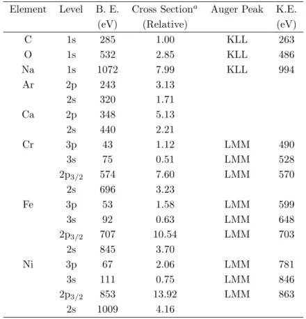
Table 1. XPS and Auger Peaks observed in Stainless Steel together with their Photoionization Cross-Sections
towards MgK α x-rays (1253.6 eV).
Element Level B. E. Cross Sectiona Auger Peak K.E.
(eV) (Relative) (eV)
C 1s 285 1.00 KLL 263 O 1s 532 2.85 KLL 486 Na 1s 1072 7.99 KLL 994 Ar 2p 243 3.13 2s 320 1.71 Ca 2p 348 5.13 2s 440 2.21 Cr 3p 43 1.12 LMM 490 3s 75 0.51 LMM 528 2p3/2 574 7.60 LMM 570 2s 696 3.23 Fe 3p 53 1.58 LMM 599 3s 92 0.63 LMM 648 2p3/2 707 10.54 LMM 703 2s 845 3.70 Ni 3p 67 2.06 LMM 781 3s 111 0.75 LMM 846 2p3/2 853 13.92 LMM 863 2s 1009 4.16 aReference 8.
Chemical State Information
Often it is desirable to identify the chemical state (charge) of the element under investigation since many of the chemical/physical properties depend on this. This information is also inherent in the derived bind-ing energy which shifts accordbind-ing to chemical and/or physical environment of the element. These so-called chemical shifts, although in principle calculable from first principles, involve many different kinds of pa-rameters, hence, are best determined experimentally. Figure 3 displays part of the XPS spectrum of an electrochemically CdTe coated films for solar energy applications. On the surface of the films both Te 3d and 4d peaks have multiple spin-orbit doublets which can be assigned to telluride (2-) and oxytelluride ( δ+) chemical states whereas both the Cd3d and 4d peaks are simple doublets assigned to cadmium (2+) chemical state. Relative intensities of an nd spin-orbit doublet corresponding to the 5/2 and 3/2 total angu-lar momentum states are given by (2x5/2+1): (2x3/2+1) = 6:4 which are separated by the corresponding spin-orbit splitting energies which are 10.4, 6.7 and 1.8 eV for the Te3d, Cd3d and Te4d levels, respectively, and the corresponding splitting is smaller than our instrumental resolution of 1.5 eV for the Cd4d level. The
chemical shift between the 2- and the δ+ states of tellurium can be determined from the energy difference between the corresponding 3d5/2 peaks as 3.4 eV where the binding energy of the oxytelluride is higher since
the electron experiences a higher potential. After removal of the nonstoichiometric surface layers by etching the stoichiometric CdTe can be observed as shown on the upper region of the figure. Determination of the optimum conditions for obtaining a stoichiometric CdTe coating (as determined by XPS) was demonstrated to be very important for performance of these solar collectors prepared by electrochemical methods9.
Cd 3d
TeO2- TeO
2-x
Binding Energy (eV)
_ _ _ 570 580 _ _ 405 415 _ _ 40 45 _ _ 8 12 _ _ _ _ _ _ _ _ _ Cd Te (as is) Cd Te (etched) Te 3d Te 4d Cd 4d
Figure 3. Relevant parts of XPS spectrum of electrodeposited CdTe on ITO substrate also before and after ion
etching.
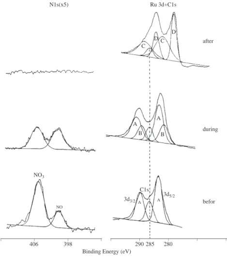
Chemical state changes can also be followed during a certain process as exemplified in Figure 4 where both Ru 3d and N1s levels are followed during thermal decomposition of a Ru(NO)(NO3)3 catalyst precursor.
Before annealing the Ru is at 4+ state (as designated by A in Figure 4) and two different nitrogens (NO3
and NO) with the correct stoichiometric ratio of 3:1 are present. During annealing NO3 is lost initially with
the corresponding shift of Ru to 3+ first (B) followed by 2+ (C) after loosing all of nitrogens metallic Ru (D) is also observed. When the same precursor is analyzed on silica support thermal decomposition is prevented as a result of a host-guest interaction and only in the presence of H2 a similar decomposition/reduction
could be realized 10.
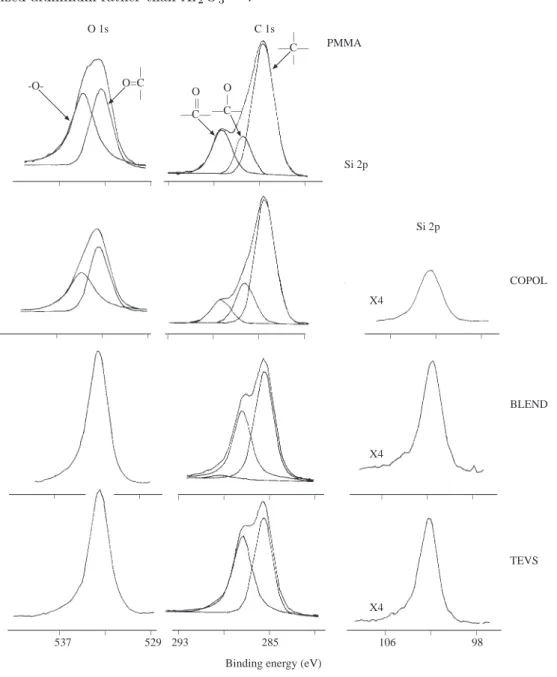
Chemical shifts in the C1s level for different types of carbon and substituents are very important in polymer characterization. Certain agents concentrate very effectively at the surface of materials which can be an asset for certain applications (and nuisance for others). Such as the case for silicon containing polymeric materials11. Due to the very low surface energy siloxane containing groups dominate the surfaces when
blended or copolymerized with other polymers. In a similar study we investigated the surface composition of the hydroxy-terminated poly(( ε-caprolactone, PCL) / poly(dimethylsiloxane, PDMS) triblock copolymers using XPS and were able to show that the PDMS microdomains were segregated in the surface region to minimize the surface energy12. The result of a similar investigation is shown in Figure 5 where part of
XPS spectra of methyl methacrylate (MMA) and triethoxyvinylsilane (TEVS) polymerized using 60Co( γ
-radiation together with their copolymers and blends are displayed. The spectrum of the blend which contains 90% PMMA and 10 % PTEVS is completely dominated by features assigned to PTEVS since the latter is very surface active. Through copolymerization in which the TEVS composition can be as high as 70% in the feed a reasonably mixed PMMA/PTEVS random copolymers can be achieved as also depicted in the figure13. NO3 NO N1s(x5) Ru 3d+C1s C D C D A A B B C1s 3d5/2 A A 3d3/2 after during befor _ _ _ _ _ _ _ _ _ 398 406 290 285 280
Binding Energy (eV)
Figure 4. Ru3d and N1s regions of XPS spectrum of a Ru(NO)(NO3)3 catalyst precursor before, during and after
annealing. As NO and subsequently NO3 are lost Ru is reduced from 4+ to metallic state successively.
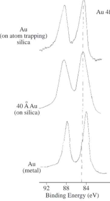
Shifts due to physical environment can also be determined as shown in Figure 6 where the binding energy of the Au4f doublet at its metallic state are displayed when gold is deposited under different conditions
14. Careful investigations also revealed chemical shifts due to particulate (cluster) size for gold colloids15.
The Auger peaks also display chemical shifts and in some cases the shifts can be larger than those on XPS peaks. Such a situation arises in the Al XPS 2p peak and the Auger KLL peak as shown in Figure 7. The chemical shift between the Al3+ (in Al
2O3) and Al0 (in metallic state) is 5.5 eV in the KLL peaks and
only 2.7 eV in the Al2p peaks. Combination of the chemical shifts in the photo lines together with those on the Auger ones can lead to another experimentally derivable parameter, the Auger parameter16 which can
give even more precise chemical/physical state information as was demonstrated for Ni pigmented Al2O3
to the anodized aluminum rather than Al2O3 17. O 1s C 1s | O=C | O || —C— | —C— | O | —C— PMMA Si 2p _ _ _ _ _ _ _ _ _ _ _ _ _ _ _ _ _ _ _ _ _ _ _ _ _ _ _ _ _ _ _ _ _ _ 537 529 293 285 106 98 X4 X4 X4 _ _ Si 2p COPOL BLEND TEVS
Binding energy (eV)
Figure 5. Ols, Cls and Si2p regions of 60Co γ -ray induced PMMA and PTEVS together with their 10% PTEVS and 90 % PMMA blend. The spectrum of the blend is completely dominated by PTEVS. Whereas the spectrum of the corresponding copolymer where the initial feed contained 70 % TEVS and 30 % MMA displays features representing both of the polymers.
Depth Information
i-Angle Resolved XPS
The position of the electron energy analyzer with respect to the sample can be altered to vary the analysis depth of a given sample as shown in Figure 8. The result is a change in the electron take-off angle and hence
a longer escape depth for electrons stemming from the layers below the surface affecting the attenuation of the intensity of the electrons belonging to bulk atoms with respect to those on the surface.
Au (on atom trapping)
silica 40 A Au (on silica) ° Au 4f Au (metal) _ _ _ 84 88 92
Binding Energy (eV)
Figure 6. When gold is deposited on silica the binding energy of the 4f levels shift about 0.7 eV with respect to
the metal although both are zerovalent. This information was used to assign the chemical state of gold deposited on an atom-trapping silica for use in signal enhancement in AAS14.
Al (anodized) Al _ _ _ _ _ _ Al2p Al (KLL Auger) _ _ _ _ _ _ _ _ _ _ _ _ 1396 1388 73 77 Al+3 Al+3 Al0 Al0 B. E. (eV) K. E. (eV) Al (Ni)
Figure 7. Al2p and Al KLL peaks of metallic and anodized aluminum samples. The metal has about 3 nm native
oxide hence peaks belonging to both Al0 and Al3+ are observed. The chemical shift in the Auger peaks are more enhanced when compared with XPS peaks. The figure also displays the spectrum of Ni-pigmented aluminum solar collector where, using the Auger parameter obtained by combining the XPS and Auger shifts, it was demonstrated that the Al resembled anodized aluminum rather than Al2O3 17.
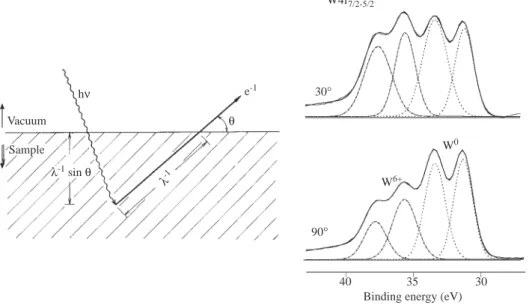
An analytical procedure has been developed to estimate the thickness by making use of such angle-dependency if the surface and bulk atoms have different chemical shifts such in the case of W4f levels of tungsten coated glasses. In Figure 8 the W4f levels at two different electron take-off angles (90◦ and 30◦) are also given where the intensity of the metal peaks are clearly attenuated with respect to oxide ones. The thickness, d, of the oxide-overlayer can be calculated using the formula;
IW Ox/IW ={1 − exp(−d/λ. sin θ)}/{exp(−d/λ. sin θ)} (2)
where λ is the attenuation length and θ is the electron take-off angle with respect to the surface normal. Using the experimentally determined parameters one can obtain a thickness of approximately 4.5 nm for this native tungsten oxide 6. This method is quick and versatile probe for deciding whether or not some
element or a certain functional group is concentrated on the surface but is applicable only to uniform layers having thickness less than 10 nm.
Vacuum Sample λ-1 sin θ θ e-1 hν λ-1 90° W0 W6+ 30° W4f7/2-5/2 _ _ _ 30 35 40
Binding energy (eV)
Figure 8. An schematic diagram of the electron take-off angle θ is shown. λ is the electron’s attenuation length.
The XPS spectra of the 4f region of tungsten-coated glass recorded at 90◦ and 30◦ electron’s take-off angles are also included. At the lower take-off angle the metallic peaks lose intensity with respect to oxide ones.
ii- Chemical and/or Ar
+Etching
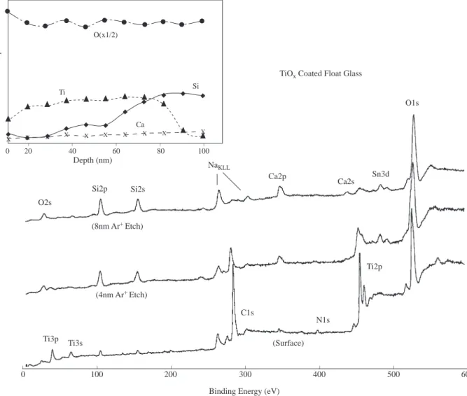
This process utilizes the layer by layer removal either by chemical or physical means and subsequent analysis by XPS or AES. Both etching processes are known to be nonstoichiometric and can lead to serious errors in chemical state determination as well as quantification if precautions are not taken. They, nevertheless, are very popular to map out the compositional variations from the surface into the bulk of the material (depth profiling). In Figure 9 spectra of an approximately 100 nm TiO2 coated glass at different etching periods
are shown. As the coating level is depleted features representative of typical float glass appear; mostly SiO2
but also Na, Mg and Ca as well as Sn which adheres to the surface of the float-glass since the molten glass is poured onto a hot liquid Sn-bath for obtaining smooth surfaces18.
X X X X X X X X X X O(x1/2) Ti Si Ca _ _ _ _ _ % Atomic Composition 100 80 60 40 20 0 O2s Si2p Si2s NaKLL Ca2p Ca2s Sn3d O1s Ti2p C1s (8nm Ar+Etch) (4nm Ar+Etch)
Ti3p Ti3s (Surface)
N1s
TiOx Coated Float Glass
_ _ _ _ _ _ _ 600 500 400 300 200 100 0 Depth (nm)
Binding Energy (eV)
Figure 9. XPS spectra of about 80nm TiO2 coated flont glass recorded at different etching periods (corresponding
to different depths from the surface)
Acknowledgments
I would like to express my sincere appreciation to my collaborators; Prof. Dr. G. C. Allen (Bristol, UK), O.Y. Ataman (METU), Prof. B.M. Baysal (Marmara Research Center), Dr. T. C¸ aykara (G. U.), Prof. H. Demiryont (S¸i¸se-Cam), Prof. Dr. O. G¨uven (H. U.), Prof. Dr. F. Kadırgan (˙ITU), Mr. S¸. Sayan (Bilkent U.) and Prof. Dr. D.O. Uner (METU) for innumerable suggestions and contributions. Financial support of T ¨UB˙ITAK through grants TBAG-˙I-15/7 and TBAG-COST-1 is kindly acknowledged.
References
1. O. Nilsson, C.H. Norberg, J.E. Bergmark, A. Fahlman, C. Nordling and K. Siegbahn, Helv. Phys. Acta 41, 1064-1095 (1968).
2. K. Siegbahn et.al. ESCA, Atomic, Molecular and Solid State Structure by Means of Electron Spectroscopy, Almqvist and Wiksells Boktryckeri AB, Uppsala (1967).
3. D.W. Turner, C. Baker, A.D. Baker and C.R. Brundle, Molecular Photoelectron Spectroscopy, Wiley-Interscience, London (1970).
4. J.H.D. Eland, Photoelectron Spectroscopy, Butterworths, London (1984). 5. G.K. Wertheim, J. Electron Spectrosc. 47, 271-281 (1988).
6. D. Briggs and M. Seah, Practical Surface Analysis, Vol.1- Auger and X-Ray Photoelectron Spectroscopy, 2. Ed., Wiley, Chichester (1996).
7. C.J. Powell, J. Electron Spectrosc. 47, 197-214 (1988). 8. J.H. Scofield, J. Electron Spectrosc. 8, 129-137 (1976).
9. S¸. S¨uzer, S¸. Kutun and F. Kadırgan, Fresenius J. Anal. Chem. 355, 384-86 (1996). 10. S¸. Sayan, S¸. S¨uzer and D.O. Uner, J. Mol. Struc. 410-411, 111-14 (1997).
11. ˙I. Yılg¨or and J.E. McGrath, Adv. Polm. Sci. 86, 1-85 (1988).
12. H.Y. Erbil, B. Yasar, S¸. S¨uzer and B.M. Baysal, Langmuir 13, 5484-93 (1997). 13. T. C¸ aykara, O. G¨uven and S¸. S¨uzer, Polymer 39, 5269-71 (1998).
14. S¸. S¨uzer, N. Erta¸s, S. Kumser and O.Y. Ataman, Appl. Spect. 10, 1537-39 (1997).
15. C. Battistoni, G. Mattogno and D.M.P. Mingos, J. Electron Spectrosc. 33, 107-113 (1984). 16. C.D. Wagner and A. Joshi, J. Electron Spectrosc. 47, 283-313 (1988).
17. S¸. S¨uzer, F. Kadırgan, H.M. S¨ohmen, A.J. Wetherilt and ˙I.E. T¨ure, Sol. Energy Mater. 52, 55-60 (1998). 18. S¸. S¨uzer, T. Voscoboinikov, K.R. Hallam and G.C. Allen, Fresenius J. Anal. Chem. 355, 654-656 (1996).