ACCELERATING PAGERANK WITH A
HETEROGENEOUS TWO PHASE
CPU-FPGA ALGORITHM
a thesis submitted to
the graduate school of engineering and science
of bilkent university
in partial fulfillment of the requirements for
the degree of
master of science
in
computer engineering
By
Furkan Usta
December 2020
Accelerating Pagerank with a Heterogeneous Two Phase CPU-FPGA Algorithm
By Furkan Usta December 2020
We certify that we have read this thesis and that in our opinion it is fully adequate, in scope and in quality, as a thesis for the degree of Master of Science.
M. Mustafa ¨Ozdal(Advisor)
¨
Ozcan ¨Ozt¨urk
Engin Demir
Approved for the Graduate School of Engineering and Science:
Ezhan Kara¸san
ABSTRACT
ACCELERATING PAGERANK WITH A
HETEROGENEOUS TWO PHASE CPU-FPGA
ALGORITHM
Furkan Usta
M.S. in Computer Engineering Advisor: M. Mustafa ¨Ozdal
December 2020
PageRank is a network analysis algorithm that is used to measure the importance of each vertex in a graph. Fundamentally it is a Sparse Matrix-Vector multipli-cation problem and suffers from the same bottlenecks, such as irregular memory access and low computation-to-communication ratio. Moreover, the existing Field Programmable Gate Array (FPGA) accelerators for PageRank algorithm either require large portions of the graph to be in-memory, which is not suitable for big data applications or cannot fully utilize the memory bandwidth. Recently published Propagation Blocking(PB) methodology improves the performance of PageRank by dividing the execution into binning and accumulation phases. In this paper, we propose a heterogeneous high-throughput implementation of the PB algorithm where the binning phase executed on the FPGA while accumu-lation is done on a CPU. Unlike prior solutions, our design can handle graphs of any sizes with no need for an on-board FPGA memory. We also show that despite the low frequency of our device, compared to the CPU, by offloading ran-dom writes to an accelerator we can still improve the performance significantly. Experimental results show that with our proposed accelerator, PB algorithm can gain up to 40% speedup.
¨
OZET
˙IS¸LEMCI VE FPGA KULLANARAK AYRıS¸ıK ˙IKI
FAZLı Y ¨
ONTEMI ILE PAGERANK ALGORITMASıNı
HıZLANDıRMAK
Furkan Usta
Bilgisayar M¨uhendisli˘gi, Y¨uksek Lisans Tez Danı¸smanı: M. Mustafa ¨Ozdal
Aralık 2020
PageRank a˘g analizinde kullanılan, her noktanın ¸cizge i¸cerisindeki ¨onemini hesaplayan bir algoritmadır. ¨oz¨unde Seyrek-Matris ve Vekt¨or ¸carpımını e¸sit olan bir problem olup aynı performans sıkıntılarından muzdariptir: d¨uzensiz hafıza eri¸simi ve hesaplama-ileti¸sim oranının d¨u¸s¨uk olması. Dahası, PageRank i¸cin hali hazırda mevcut bulunan Alanda Programlanabilir Kapı Dizisi (FPGA) hızlandırıcıları ya ¸cizgenin tamamının hızlandırıcının hafızasında bulunmasını gerektiriyor ya da var olan kaynakları yeteri kadar etkili kullanamıyor. Yakın zamanda yayınlanmıs olan, Yayılma Tıkama (PB) metodu PageRank’i gruplama ve toplama adı verilen iki adıma ayırarak performansını arttırmaktadır. Biz de bu makelede PB algoritmasının ilk a¸saması FPGA ¨uzerinde ikini a¸saması ise Merkezi ˙I¸slem Birimi (CPU) ¨uzerinde ayrı¸sık bi¸cimde y¨uksek hacimli olarak ¸calı¸saca˘gı bir tasarım sunduk. Daha ¨onceden var olan y¨ontemlerin aksine bizim tasarımımız herhangi boyuttaki ¸cizgeleri, sadece hızlandırıcı ¨uzerindeki hafızayı kullanarak i¸sleyebilmektedir. Deneylerimiz sonucunda elde etti˘gimiz sonu¸clar bize hızlandırıcımızın %40’a kadar hız artı¸sı sa˘gladı˘gını g¨ostermektedir.
Acknowledgement
First of all, I am very grateful to my advisor Mustafa Ozdal for his support and patience. Also, I would like to thank my jury members, Ozcan Ozturk and Engin Demir, as well for their interest and feedbacks.
I am also thankful to Andrey Ayupov from Intel for the mentoring and this opportunity they provided.
Lastly, I would like to offer my gratitude to my family and friends, who ex-pressed their support throughout all these years.
Contents
1 Introduction 1 2 Problem Description 3 2.1 Available Optimizations . . . 6 2.2 Two-Phase algorithm . . . 8 2.3 Accelerating PageRank . . . 10 3 Proposed Accelerator 12 3.1 Device Details . . . 13 3.2 Input Module . . . 14 3.3 Processing Unit . . . 15 3.4 Splitter . . . 15 3.5 Output Buffers . . . 17 3.6 Resource Usage . . . 17CONTENTS vii
4 Design Choices 19
4.1 Graph Layout . . . 19
4.2 IP Cores . . . 19
4.3 Deterministic Write Order . . . 20
4.4 Bandwidth Utilization . . . 21 4.5 Concurrent Execution . . . 22 5 Benchmarks 24 5.1 Experimental Setup . . . 24 5.2 Baseline Algorithm . . . 25 5.3 Parameter Selection . . . 25 5.4 Results . . . 26 5.5 Discussion . . . 27 6 Existing Solutions 30 6.1 Proposals with Custom Hardware . . . 30
6.2 Proposals with Limitation on the Graph Size . . . 31
6.3 Frameworks . . . 32
6.3.1 IP Cores for Graph Kernels . . . 32
CONTENTS viii
6.3.3 Hitgraph . . . 33
6.3.4 GraphOps . . . 33
6.3.5 GraphPulse . . . 34
List of Figures
2.1 Sparse-Matrix Vector Multiplication in Pull direction . . . 5
2.2 Sparse-Matrix Vector Multiplication in Push direction . . . 6
2.3 Visualization of cache blocking method . . . 7
2.4 Illustration of the Two-Phase Propagation Blocking Algorithm . . 9
3.1 High-Level Overview of the Accelerator . . . 13
3.2 Architecture of the Processing Unit . . . 15
5.1 Execution Time . . . 28
List of Tables
5.1 Graphs Used for the benchmarks . . . 25
5.2 Execution time (ms) per iteration . . . 26
Chapter 1
Introduction
With the emergence of massive datasets, there has been a surge of distributed graph processing framework proposals [1, 2, 3, 4, 5].
Distributed frameworks can provide performance improvements, however net-work communications add a significant overhead. This, coupled with low computation-to-communication ratio and irregular memory access patterns of many graph algorithms still makes shared-memory systems a viable option. More-over existing server-grade DRAM memories can store billions of edges and increas-ing trend of cloud computincreas-ing makes these hardware readily available. Although shared-memory systems have significantly lower communication cost they still suffer from the same memory access problems due to the nature of the graph algorithms. To alleviate this problem, there have also been number of accel-erator proposals for graphs, mainly using Graphics Processing Units (GPU) or Field-Programmable Gate Arrays (FPGA) [6, 7, 8]. However, neither FPGAs nor GPUs are well-suited as graph accelerators. Both of them have low memory capacity and geared towards more computation-heavy problems. FPGAs can ex-ecute complex combinational operations whereas GPUs can exex-ecute multitude of threads in parallel.
large-scale social networks to determine the relative importance of each vertex in the graph. Similar to others it suffers from poor spatial and temporal local-ity problem so much that memory communication is often the bottleneck [9]. Although there exists a number of preprocessing optimization proposals, many real-world graphs are irregular and scale-free, and thus hard to partition or re-order. Cache blocking techniques can improve the performance, however inherent irregularity still results in inefficient bandwidth utilization [9]. Recently a number of two-phase algorithms that are aimed at improving locality have been proposed. These algorithms operate by splitting existing PageRank algorithm into binning and accumulation phases while aiming to decrease random memory accesses, and thus, improve the bandwidth utilization [8, 9, 10]. Although, temporal storage in-between phases increases the total number of memory accesses, it improves the performance by replacing random accesses with contiguous ones.
In this paper, we propose an FPGA implementation for the binning phase of the two phase algorithm. With this design, we will also be able to demonstrate that by adapting an existing algorithm to the underlying platform we can still gain considerable performance improvements despite the hardware not being suitable for this kind of operation.
Unlike the existing PageRank implementations on FPGA [6], our design can run at almost full throughput and only requires a small amount of on-chip mem-ory. Moreover, both the number of execution units and on-chip memory usage is configurable. We evaluate our accelerator using a combination of real-world and synthetic graphs provided by GAP Benchmark Suite [11]. Our main contributions are:
• We develop an FPGA accelerator for the binning phase of the 2-Phase PageRank algorithm that can achieve 200MHz clock rate.
• We provide an heteregeneous CPU implementation for the accumulation phase
• Compared to the CPU-only implementation we can achieve 70% speed im-provement on average
Chapter 2
Problem Description
PageRank is a network analysis algorithm mainly utilized by search engines to calculate the relative importance of each webpage and determine their ranks. It builds the graph using sites as vertices and links between them as edges. Values produced by each iteration of the algorithm corresponds to the probability of a random surfer following the links to end up at that particular vertex. Although there are other means to calculate or approximate the values, in this work we will use the formula for the iterative method.
P R(u) = 1 − d |V | + d × X (v,u)∈E P R(v) dout(v) (2.1)
In Equation 2.1 d is the damping factor and usually it is set to 0.85, and dout(v) is the number of outgoing edges vertex v. To put it simply we can say that the rank of a vertex is the summation of the scaled ranks of its incoming edges. Multiple iterations of the equation is performed until convergence. In formula 2.1, the input graph can be represented using a sparse matrix A where Aij denotes an edge from vertex i to vertex j. This way it is possible to rewrite
the distribution and the reduction of the ranks as an application of SpMV.
P R = (1 − d) × AT × P R (2.2)
implementations and vice versa. However, in this paper we will focus on PageR-ank applications.
Listing 2.1: PageRank pull direction I n p u t : G(V, E) Output : Rank [ ] f o r e a c h v e r t e x v in V do c o n t r i b u t i o n s [ v ] = Rank [V] / dout ( v ) f o r e a c h v e r t e x v in V do sum = 0 f o r e a c h i n c o m i n g n e i g h b o r u o f v e r t e x v do sum += c o n t r i b u t i o n s [ v ] Rank [ v ] = ( 1 − d ) / |V| + d ∗ sum
Listing 2.2: PageRank push direction I n p u t : G(V, E) Output : Rank [ ] sums [ 0 . . V] = 0 f o r e a c h v e r t e x v in V do c o n t r i b u t i o n = Rank [V] / dout ( v ) f o r e a c h o u t g o i n g n e i g h b o r u o f v e r t e x v do sums [ u ] += c o n t r i b u t i o n f o r e a c h v e r t e x v in V do Rank [ v ] = ( 1 − d ) / |V| + d ∗ sums [ v ]
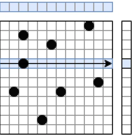
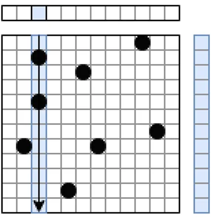
A simple PageRank algorithm can be implemented in either pull or push di-rection. When the Matrix Vector multiplication terminology is used to represent these algorithms, pull direction corresponds to a row-major matrix traversal, and similarly, push direction corresponds to a column-major traversal. These visu-alizations for pull and push directions can be seen in Figure 2.1 and Figure 2.2 respectively.
The Pseudo-code for a single iteration of the methods discussed are given in Listing 2.1 and 2.2, respectively. These functions can be called inside an another
Figure 2.1: Sparse-Matrix Vector Multiplication in Pull direction
loop either for a fixed number of times or until convergence. In both directions outer loop of the procedure iterates over the vertices of the graph. However, in the inner loop we can either iterate over the incoming edges of the current vertex and read (pull) their contributions, or iterate over the outgoing edges of the vertex and write (push) the contribution of the current vertex there. Regardless of the direction, they will both calculate the same ranks. The main difference between the two is where they reuse the existing variables and where they perform mem-ory accesses. Pull direction reuses the ”sum” variable and performs a memmem-ory access while reading contributions, on the other hand push direction reuses the ”contribution” variable and performs a memory access while writing to the sums variable. The advantage of pull direction over push direction manifests itself in the case of multiple threads. In push direction, there will be multiple writes to the same index of the result vector, requiring atomic operations to prevent data races. On the other hand when using a push-direction one can benefit from the active set optimization, where at each iteration instead of traversing all the vertices the algorithm can drop the ones that have already reached an equilibrium. However, there have been a recent proposal in this area that uses a different storage format which enables active set optimization to pull direction as well [12, 13]. Moreover, there are also existing proposals on a more hybrid approach where the decision can change between the iterations [14].
Figure 2.2: Sparse-Matrix Vector Multiplication in Push direction
2.1
Available Optimizations
Although the main formulation of the PageRank is quite simple there are many optimizations available that can affect the performance significantly without al-tering the core of the algorithm. In most cases there is no one-size-fits-all for these algorithms and most of them are dependent on the use-cases and graph properties such as maximum degree, average degree, percentage of the non zero elements, distribution of those elements so on and so forth.
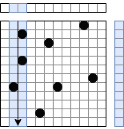
Since at each iteration the shape of the graph and the iteration order stays the same and there are no conditional memory requests, it is quite easy to for-mulate the number of reads and writes [15]. However, those numbers do not directly translate to the performance metrics due to cache locality. One of the optimizations to improve the cache locality is Cache Blocking technique. In this optimization, instead of using the whole vector one divides the vector into multiple segments where each part can fit into cache and proceeds accordingly. Represen-tation for this optimization is available in Figure 2.3. However, one drawback of this optimization is that this will improve the locality on the input vector while disturbing the locality of the output vector. The writes to a single index of the output vector will be separated. Although, it is possible to compromise both ways and divide the matrix into a grid and do the cache blocking both ways, these optimizations are highly dependent on the graph topology [16].
Figure 2.3: Visualization of cache blocking method
Memory accesses we are doing in both variations are not sequential, and thus, performance is affected greatly by the layout of the graph [9]. Reordering the graph is one way to improve the cache locality and possibly increase the per-formance benefits of the cache blocking and other similar algorithms. Although graph reordering is mostly done as a preprocessing step [17, 18] it is possible to do it as part of the scheduling algorithm as well [19]. Run-time reordering algorithms can utilize performance counters to make guided decisions [20].
One advantage of the reordering is that it also enables graph for better par-titioning. Partitioning can be the crucial part of the algorithm for architectures that utilize many number of threads such as GPUs. As the number of working threads increase, the need for the synchronization points will also increase and a good partition might reduce the number of inter-thread communication [21, 22]. It can also be useful for FPGA implementations as well. Although the number of processing units for FPGAs is not as high as GPUs, in this case the problem would be the memory bandwidth. By keeping the destination of the write mes-sages close to each other one can reduce the intermediary values on-chip and only flush the data at the end [23].
Last but not least it is also important to keep in mind that although there are a few graph layouts that are quite popular such as CSR/CSC, ELLPACK and COO [24], there are myriad of available formats as well, depending on the use case. There are compressed data formats that might be beneficial for FPGA
architectures that keep the vector data on fast-memory [25, 26] as long as en-coding and deen-coding the data does not hinder the performance. There are also formats that utilizes existing SIMD architectures [27, 28]. One might also use a generalized storage format that aims to cater many kind of layouts and even in some cases both sparse and dense matrices [29] which might be quite beneficial for a generalized framework [30].
2.2
Two-Phase algorithm
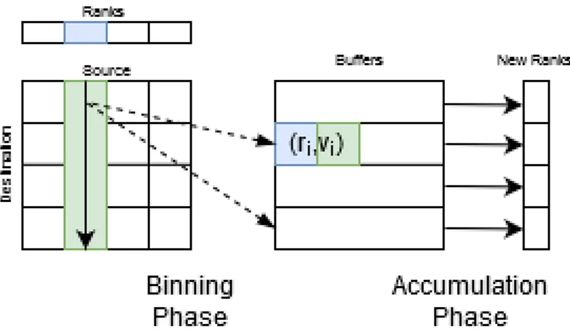
To improve the locality and reduce the random memory access bottlenecks, Two-Phase algorithm are proposed by various groups with different optimizations [10, 8, 31]. Since the main idea behind all three papers is quite similar we will use the terminology from Beamer et. al in here. A pseudo-code for the algorithm is given in Listing 2.3. The idea behind the algorithm resembles cache blocking; however instead of blocking the graph itself, it blocks the propagation of the ranks (vertex values). The first phase of the algorithm, called binning, is quite similar to the push-based algorithm. It iterates over the vertices and calculates their contributions; however instead of writing these contributions directly to their outgoing neighbors, this time it stores the values as contribution and destination pairs to intermediate buffers. Although layout-specific vertex-to-buffer mappings can be used, in this work we chose to simply divide the vertex set into B groups, where B is the number of buffers. Hence, our mapping function is defined as Bid(v) = v
B, where Bid(v) is the index of the buffer v is assigned to
In the second phase of the algorithm, called accumulation, each bucket is processed separately and the contribution values are added into the corresponding sums defined by the second element of the pair. Unlike the multi-threaded push-based algorithm, in this phase there is no need for a locking mechanism as long as each buffer is processed by a single thread. Since there is only a single buffer corresponding to a vertex, buffers will be able to write to their parts of the memory exclusively.
Figure 2.4: Illustration of the Two-Phase Propagation Blocking Algorithm
Listing 2.3: 2-Phase PageRank I n p u t : G=(V, E ) , B ( number o f b u f f e r s ) Output : Rank [V] sums [ 0 . . V] = 0 b u f f e r s [ 0 . . B ] # B i n n i n g Phase f o r e a c h v e r t e x v in V: c o n t r i b u t i o n = Rank [V] / dout ( v ) f o r e a c h o u t g o i n g n e i g h b o r u o f v e r t e x v : append ( c o n t r i b u t i o n , v ) t o b u f f e r s [ v / B ]
# Accu mul ati on Phase f o r e a c h i in 0 . . B :
f o r e a c h ( c o n t r i b u t i o n , v ) in b u f f e r s [ i ] : sums [ v ] += c o n t r i b u t i o n
f o r e a c h v e r t e x v in V:
Rank [ v ] = ( 1 − d ) / |V| + d ∗ sums [ v ]
The advantage of splitting the algorithm into two phases is that at each phase we are reducing the span of the memory we are accessing. In the binning phase,
instead of the full range of memory we will be accessing only B locations since both writes to the buffers and reads from the rank arrays will be sequential. Similarly in the accumulation phase, each bucket will be responsible from |V |/B locations, and again reads are sequential leading to higher spatial locality. Note that, while choosing the number of buffers there will be a trade-off. If B is small enough we can fit all B partial cache lines into cache during the binning phase. However, a small B might hurt the performance of the accumulation phase since it increases the memory range accessed by each buffer.
The downside of using buffers for the PageRank algorithm is the extra mem-ory overhead and the increased number of load and store operations. However, Beamer et. al. concludes that despite the increase in the number of memory accesses, propagation blocking still communicates less than cache blocking when the graph is sparse enough [31]. As for the memory requirements there are opti-mizations proposed in both the original paper and the follow-ups that improve the necessary memory requirements, we will be discussing these in chapter 4. One optimization that is not shown in the Listing 2.3 is separating the destination indices from the contribution values in the buffer. As stated earlier, since the graph layout is fixed, we will be traversing the graph in the same order at each iteration; and thus, contents of the buffer for the destination parts will be the same at each iteration. Therefore it is possible to calculate those values only once as part of the first iteration and reuse the same indices later on. Although this does not reduce the memory requirement, it reduces the amount of data written to DRAM and improves performance.
2.3
Accelerating PageRank
Recently, there have been many proposals using FPGAs for graph processing [32, 33, 34, 35]. One advantage of the FPGAs is that they usually run at lower frequencies and thus consume less power than CPUs and GPUs [36], though this also means that they provide less compute power than their counterparts. How-ever thanks to their reconfigurability, it is possible to optimize the algorithms at
hand to the hardware and adapt the hardware to the algorithms as well. One important drawback of using an FPGA is the small on-chip memory capacity. Unlike GPUs which utilizes gigabytes of on-board memory and higher memory bandwidth, FPGAs usually have less resources available. That is why, it is al-most impossible to operate on large chunks of data while maintaining full memory bandwidth, instead most algorithms have to be implemented in a streaming man-ner.
Chapter 3
Proposed Accelerator
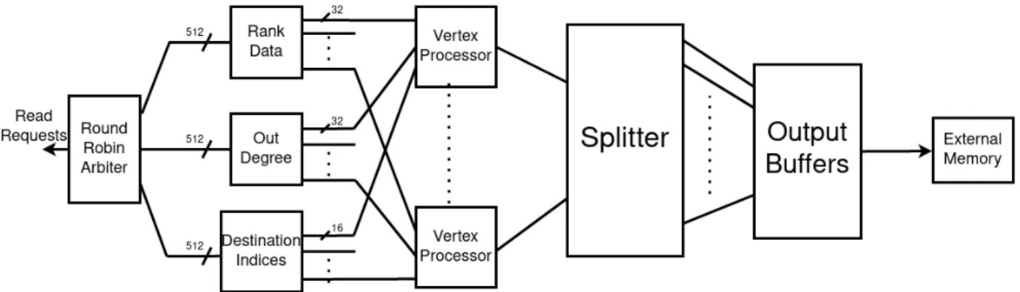
As reported in [31] Propagation Blocking algorithm yields significant performance improvements especially for large graphs. By introducing a temporary buffer and splitting the algorithm into two stages, PB can utilize a significant portion of the available memory bandwidth and also opens possibilities for concurrent execution for both within a stage and between stages. To improve the performance of the algorithm even more, we decided to introduce an accelerator and execute the two stages concurrently, one in FPGA and the other on CPU. Fully utilizing the memory bandwidth of an accelerator is a tough problem due to scarcity of available resources on the device. On-chip memory capacity and availability of logic resources limits our abilities to implement the existing algorithms as-is, since we are not able to store the whole matrix nor the vector on the FPGA. However, binning phase of the 2-Phase algorithm only performs sequential reads and for writing to the main memory we do not need to store the temporary buffer wholly on the FPGA we can store chunks of it and flush to the main memory as they are full to open space and reuse it. This way we can design a streaming algorithm that only requires a small amount of on-chip memory. As for the accumulation phase, we used a multi-threaded CPU implementation, where each thread is responsible for one of the buffers to avoid the need for locking or atomic writes. With a synchronization mechanism, that updates the status of the intermediate buffers, between the host and the accelerator we can make two stages of the algorithm
Figure 3.1: High-Level Overview of the Accelerator
execute concurrently.
A Detailed architecture of the processing unit is given in Figure 3.1. There are 4 main modules in our design: Input module, Vertex Processor, Splitter, and Output Buffers.
3.1
Device Details
For the accelerator device we used Arria 10GX 1150 (10AX115U3F45E2SGE3) provided by Intel FPGA Acceleration Hub [37]. Communication with the external memory is done by using the libraries provided by Intel [38, 39]. Even though the device is capable of running at 400MHz, our design operates at 200MHz. However, this does not hinder our performance, since SpMV problem is not computation bound we are not losing any performance as long as we are able to saturate the available memory bandwidth.
Memory blocks provided by the FPGA are called M20K and they have the capacity of 20480 bits. The width of each memory block is configurable, although we often used 16 or 32. Although M20K blocks provide multiple operating modes, we only used a dual-port mode with single-read and single-write. Results of the read requests were only available in the following cycle and our design handled it with pipelines when necessary. Read-during-write was an undefined behavior and
we had to do forwarding, or in some cases, stalling to handle this case. Although these details are common for most of the FPGA on-chip memory blocks, since it affected our algorithmic choices we decided to spell it out. Input interface we are using operates at cacheline granularity thus all the read responses and write requests contain 512 bits of data. Since it is not possible to store 512 bits directly on a single M20K block, we needed to partition the data into several blocks and merge back when requested. Thus, even though buffer sizes in both input and output modules are configurable they both require at least fourteen M20K blocks.
3.2
Input Module
We have four input streams two of which correspond to the vertex data: current rank and the number of outgoing edges of a vertex. The other is for the edge data that corresponds to the destination index. Lastly, there is an input stream for the CPU synchronization, which will be explained later. Each stream consists of multiple channels and each channel is connected to a single Vertex-Processor module. Since we are using a fixed partition for the graph, at initialization time we provide the number of vertices and edges each channel needs to process. This way, Input module can maintain which input belongs to which channel. Furthermore, this module also handles misaligned read requests.
Due to the nature of the underlying hardware, often times memory responses are received out-of-order. In order not to interfere with the traversal order, we assign each memory request a tag and these tags are received back alongside the responses. Later on, we store the response data in a temporary buffer using the tag value as an index, and thus, put them in-order. As stated in the previous section, to store the cachelines we need to split the data into 13 40-bit width M20K blocks, each of which with 512 element capacity. However, these buffers are shared between the members of a processing group which is usually 8 or 16.
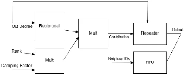
Figure 3.2: Architecture of the Processing Unit
3.3
Processing Unit
Vertex Processor receives three inputs from the input module: rank of a vertex, number of outgoing edges, and indices of its neighbors. Although it performs two multiplications and a single division, it requires pipelining since it is not possible to do even one of the operations in a single clock cycle. While it calculates the reciprocal of the out-degree, in a parallel pipeline it multiplies the rank data with the damping factor. When the reciprocal is ready, it gets multiplied with the result of the first multiplication. Even though reciprocal operation takes slightly more number of cycles than the multiplication, we can still maintain an initiation interval of 1 with a small FIFO at the end of the first multiplication operator. After calculating the contribution of a vertex, it repeats that value as an output for each of the outgoing vertices. Since all three channels are received continuously and independent of each other, a simple synchronization between the vertex and edge data is necessary.
3.4
Splitter
Splitter module contains the mechanism that maintains the pre-determined traversal order. We have multiple instances of processing units and these do
not operate at a fixed rate due to various issues such as back-pressure, out-of-order responses, varying response times, and unbalanced graph layout. As stated earlier, Input module fixes the out-of-order responses, and response times. How-ever it only guarantees an order within a single channel and not between channels. Enforcing that would complicate our design and more importantly could lead to under utilization. Instead of fixing this problem at the input stage we decided to fix the problem on the other end. Splitter module here acts as a barrier between the processing units and memory modules and ensures that each processor has an output before progressing further. This way, we can ensure that hardware re-lated delays will not introduce any non-determinism. This method as well, affects the utilization however putting the synchronization at the end enables pipeline stages to be filled sooner. Putting a FIFO between the Vertex Processors and the Splitter module makes the effect it has on the performance negligible.
In addition to synchronization, Splitter module also does reordering of the outputs to match their corresponding buffers. Originally this was the reason this module got its name, since it would receive a contribution and destination index pair but would split the pair and only let one of them to pass through. Even if we have the same number of processing units as the intermediate buffers, processing units do not have a corresponding buffer. Each processing unit is responsible of a set of vertices and each vertex in this set can have various outgoing edges. For this reason, each processing unit should be able to write to any buffer. Since any unit can write to any buffer, it is also possible for multiple vertices to output contribution value for the same buffer. In this case, Splitter module gives priority to the vertex with the lower ID and sends the others in the following clock cycles. We cannot write all of them at once because as mentioned earlier memory blocks we use have a single read and write port. Note that conflict resolution is done by reducing the throughput of the module. This also leads to our algorithm to be prone to perform worse on graphs with high conflict, since the module would not be able to process all the incoming vertices at each cycle. However, as explained in Section 2.1 these layout problems can be alleviated on the software side with graph re-ordering and better partitioning models without requiring a change in the design.
3.5
Output Buffers
As for the final module we have the output buffers which contain the contribution data. Each buffer has a single M20K memory block which can hold 32 cache-lines. Every time a buffer fills 4 cache-lines it flushes its data. The reason for this particular number is explained in Section 4.4. Normally this module would be a thin-wrapper around the system provided M20K blocks, however storing cache-lines directly on the BRAM requires 14 blocks per buffer which we cannot afford. Instead of having a separate memory block per buffer, we decided to instantiate memory blocks per cache-line element and share those among the buffers. In other words, ith memory block contains the ith element of the cache-line that
is going to be flushed. Each instance of this module consists of 16 buffers that shares the same memory blocks. This way instead of using 14 × 16 = 224 blocks we are only requiring 16 per instance.
In addition to memory management logic, this module also periodically notifies the host by writing the number of processed cachelines to a predefined location. Host program reads this counter and continues processing from the last location. This buffer is treated as a circular buffer, and host side also notifies the FPGA by writing how much it had processed. The notification from the host is necessary to prevent buffer overruns, we compare it with ours to determine the remaining capacity and stall the corresponding buffer until host catches up and frees up more space.
3.6
Resource Usage
In our design most required resource on the FPGA is M20K modules. Since that would possibly be the bottleneck when porting this accelerator to other devices we decided to provide the resource requirements of our architecture.
• Each Input module requires 9 BRAM Modules, and there are 3 Input mod-ules
• Each Processing Unit requires 4 BRAM Modules: 1 at the end of the first multiplication, and the other three is for each input.
• Each Splitter requires BRAM Modules equal to the number of output buffers, this is to reduce the effects of the aforementioned conflicts. This can also, possibly, be solved with a more effective conflict-resolution algorithm. • Each Output Buffer requires 14 BRAM Modules
• For the best performance we need 64 Processing Units in total, which can be achieved either using 8 or 16 groups where each group has a size of 8 and 4, respectively. In total for the former we would need 648 memory blocks and for the latter we require 488.
• Overall the number of BRAM modules needed is (45 + Group Size) × N umber of Groups.
Chapter 4
Design Choices
4.1
Graph Layout
For the graph representation, we initially used Compressed Sparse Row (CSR) format. However we decided that it was providing more than what we needed and a simpler format could be better suited. Since we were accessing both vertices and edges consecutively on the FPGA and random access was not a requirement on the host side, we decided to use a layout that corresponds to the input channels on the FPGA side. Thus, we store 3 arrays containing the ranks and the outgoing degrees of the vertices, and destination indices for the edges. Note that, this is not a hard requirement for the algorithm and to support other formats one would only modify the Input module as the rest of the design only requires an (edge, contribution) pair.
4.2
IP Cores
For the arithmetic operations in the vertex processor, we used fixed-point arith-metic instead of floating point, to make the implementation of the aritharith-metic
operations simpler. Although fixed-point IP cores were available on the test de-vice, we decided to implement it ourselves using a deeply pipelined approach with 1-element per cycle initiation interval to not throttle ourselves. As for the mem-ory modules, we exclusively used memories with a single read and single write port. These were occasionally used to implement a FIFO or a shift-register but most often they were used as-is. Although, we implemented these memories us-ing a register array directly, Quartus development tool [40] was able to map our implementations to the existing IP blocks on the device. This way, our source code stayed portable while also benefiting from the available resources.
4.3
Deterministic Write Order
The Synchronization mechanism provided by the Splitter module is explained in Chapter 3. Main benefit of this synchronization is that we can omit the destination indices while writing the contributions. In the accumulation phase, host side needs to read these pairs and add the contribution values to the rank of the corresponding vertex. The reason for that is that the layout of the graph we are using will not change in-between or during each iteration, and we are using a static partitioning scheme in the case of multiple binning threads. After the first iteration, destination vertices will stay the same and we will be writing redundant data. Calculating it once on the host side at the beginning of the computation, and reusing it when necessary greatly improves our results.
Although checking the iteration count and omitting the destination indices is possible to do in FPGA, the mechanism for those checks and calculations would still affect the timing and area usage, we decided to implement this optimization as a preprocessing pass on the host side. This is just a linear traversal and does not modify the graph in any way. CPU-side needs to be aware of the number of processing groups and size of each group to be able to correctly determine the order. Unfortunately, this means that host needs to be aware of the details for the accelerator. However, this dependency also enables us to do an extra optimization. In the original implementation, each destination address would
correspond to 16 bits, which increases the write memory load by 50%. In our case, we only need the write index within the processing group, which is usually 3 or 4 bits since we obtain almost optimal performance when groups size are either 8 or 16. Note that, if the original destination indices are necessary for further work, this optimization requires an additional storage. However, it is possible to disable it at the cost of an increased number of memory requests without changing the design.
4.4
Bandwidth Utilization
Operating at 400MHz the memory controller connected to our accelerator can process a single read/write request each cycle. Since our design runs at 200MHz, we would need to produce two read and two write requests each cycle to be able to run at full speed. These requests are then connected to a clock-domain crossing FIFO that is able to send them one at a time.
Vertex processor described in Chapter 3 reads one vertex at a time, however it outputs at edge-level. Since the memory operations are done at cache line granularity, we need to produce at least two cache lines, i.e. 16 edges, at each clock cycle. That is why we need at least 16 vertex processors to saturate the memory bandwidth. However depending on the graph layout there can be congestion on the Splitter module described above, or there might be vertices with no outgoing edges which costs a cycle. To compensate for the stalls, we instantiate 64 vertex processors, which are divided into 4 groups each with size 16. This way we can connect each group to a separate IO port provided by the framework to better utilize the memory bandwidth.
As stated above the device memory controller can only send one read request at a time, however thanks to an option provided by the underlying device, it can request 4 consecutive cache lines instead of just one. This does not increase our bandwidth since responses are still receive one-at-a-time, but it reduces the amount of idle time. By always issuing 4 cache line requests we can use the
outstanding memory request buffer as if it had 4 times the actual capacity. In-stead of switching at runtime between single cache line requests and 4 cache line requests, we add some extra padding at the end of the partitioned arrays and round up while reading, whereas buffer the write requests on the output side to ensure an always 4 cache line requests. The buffering on the output side increases our storage usage since the data associated with the requests are 512-bit each, however variable sized read requests would significantly increase the design of our Reader modules.
4.5
Concurrent Execution
The two stages of the algorithm can be viewed as a Producer-Consumer prob-lem, whose executions can be overlapped to reduce the idle time and improve the performance. To do so, we employed a concurrent execution model that is heav-ily inspired by a recently published algorithm [41]. In the proposed algorithm, authors use a number of fixed size buffers and two queues for synchronization. One of the queues stores the indices of the buffers filled by the binning thread, and the other stores the indices processed by the accumulator thread. This way, both stages can execute concurrently and we can reuse the storage that has been processed and readily available. To implement this algorithm on a heterogeneous system we decided to use a circular buffer instead of two separate queues. Syn-chronization between the host and accelerator uses a polling technique. FPGA periodically writes the number of processed vertices to a predetermined address to notify the host. CPU thread wakes up, checks the number and if there are new vertices, accumulates them. Similarly, host side notifies the FPGA for the pro-cessed data so that FPGA can start reusing from the beginning when the buffer is full. Both the period of the updates and the buffer capacity is configurable. Unlike the originally proposed concurrent execution model, in our method we always write to and read from the buffers in linear order. In the case that the storage for a buffer is full, FPGA stalls the execution for that buffer until new space gets freed.
One important advantage of using circular buffers is to reduce the memory requirement of the temporary storage. In both Beamer et al. [31] and Buono et al.[10], intermediate buffers have the capacity to hold the whole matrix, which doubles the memory requirements for the edge data. In our design we only require a fixed sized and configurable buffer
After ensuring the synchronization between the actors, executing the phases concurrently is quite trivial. Shared data is only written by the FPGA and read by CPU. Parallel implementation on the CPU-side is done using OpenMP. We fixed the number of threads to the number of available CPU cores, and apart from that all the other OpenMP parameters as left as-is. Each thread is responsible from a group of buffers, and also each buffer can only be accessed by a single thread. Moreover, each vertex is assigned to a single buffer, requiring no locking or atomic updates when writing to the buffers. Similarly, on the FPGA side each processing group is responsible from its own set of buffers and there is no need for synchronization between the groups.
Chapter 5
Benchmarks
5.1
Experimental Setup
Benchmarks are performed on a Xeon CPU (E5-2600v4) with 24 cores and 64GB DRAM. Both host side of our proposed algorithm and the baseline algorithms are tested on the same device We implemented the host side and baseline algorithms using C++ and compiled with g++ version 9.1.1 using optimization flag -O3. For the accelerator we used Arria 10GX 1150 (10AX115U3F45E2SGE3). Accelerator is implemented using Chisel Language [47]. Bitstream for the FPGA is generated using Intel Quartus Prime version 16.0 with optimizations enabled [40]. Broadwell Xeon CPU (E5-2600v4) is used to run the baseline algorithms and the host code of our design.
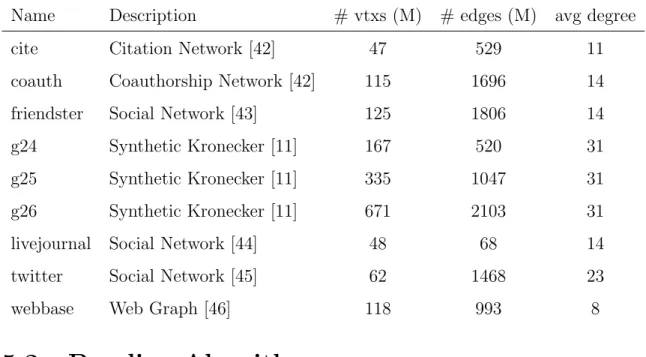
For the graphs used in our experiments, we have chosen the scale-free graphs used in the original 2-Phase PageRank algorithm [31]. Tree of these graphs (g24, g25, g26) are Kronecker graphs that are similar to the inputs of Graph500 [48] and generated synthetically by using the software provided by Berkeley GAP Benchmark Suite [11]. The details of these datasets are given in table 5.1. The other 6 test cases are datasets that are collected on real-world use cases.
Table 5.1: Graphs Used for the benchmarks
Name Description # vtxs (M) # edges (M) avg degree cite Citation Network [42] 47 529 11 coauth Coauthorship Network [42] 115 1696 14 friendster Social Network [43] 125 1806 14 g24 Synthetic Kronecker [11] 167 520 31 g25 Synthetic Kronecker [11] 335 1047 31 g26 Synthetic Kronecker [11] 671 2103 31 livejournal Social Network [44] 48 68 14 twitter Social Network [45] 62 1468 23
webbase Web Graph [46] 118 993 8
5.2
Baseline Algorithm
As baseline, we used the CPU implementation of the 2-phase algorithm [31]. The source code is the same as the one used in [41].
We also provide comparisons with the concurrent implementation in [41]. Al-though they employed a more efficient algorithm due to a more compact layout and better utilization of the concurrency, we provide the comparisons to show that it is possible to achieve comparable results using a simpler algorithm as well as to show that there is still room for improvement in our accelerator design.
5.3
Parameter Selection
We used all 28 threads available for parallel execution. Although performance of the host side could possibly be improved using a dynamic reader/writer pool and make host side contribute to the first phase as well, we opted for a simpler model.
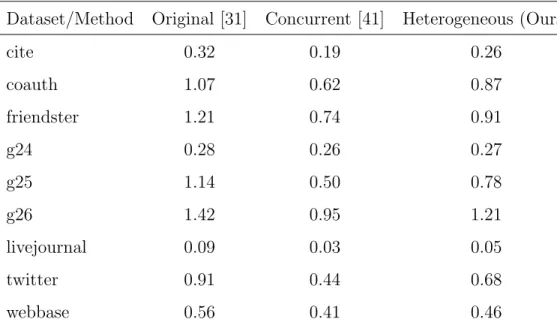
Table 5.2: Execution time (ms) per iteration
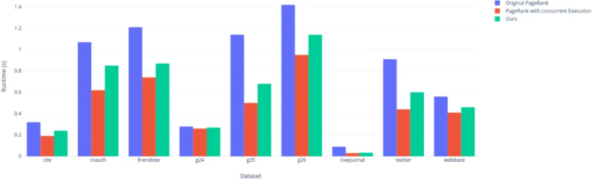
Dataset/Method Original [31] Concurrent [41] Heterogeneous (Ours)
cite 0.32 0.19 0.26 coauth 1.07 0.62 0.87 friendster 1.21 0.74 0.91 g24 0.28 0.26 0.27 g25 1.14 0.50 0.78 g26 1.42 0.95 1.21 livejournal 0.09 0.03 0.05 twitter 0.91 0.44 0.68 webbase 0.56 0.41 0.46
Since the graph is logically partitioned for each buffer, we statically mapped those buffers to a single thread. For the buffer size, in our experiments we’ve seen that we can mostly avoid stalling when the buffers contain around 100K elements, depending on the layout. However, we opted for 128K to reduce the synchronization traffic, and to be on the safe side assuming that the difference in the storage would be negligible. Instead of tuning each parameter for each dataset we picked one that works well for most and applied these parameters to all of the tests. In this case, it means 128K elements for the buffer capacity and FPGA signals the host side at every 64K elements processed.
5.4
Results
Results in Table 5.2 are collected by averaging the execution times of 50 iterations. As mentioned throughout the paper, we can also observe from Table 5.3 that there is no direct correlation between the graph size and the speedup. Even on the ones that follow a similar distribution, Kronecker graphs, we cannot assert an exact prediction on what the speedup would be. However, it is clear from
Table 5.3: Throughput Ratio (Higher is better)
Dataset/Method Original [31] Heterogeneous (Ours)
cite 1 1.23 coauth 1 1.22 friendster 1 1.32 g24 1 1.03 g25 1 1.46 g26 1 1.17 livejournal 1 1.8 twitter 1 1.33 webbase 1 1.22
the execution times that, although occasionally small, on these datasets FPGA acceleration always provided performance improvements. Since the number of memory requests are quite similar to the original PageRank algorithm, we decided to omit that in our comparisons.
5.5
Discussion
Looking at the results we believe that FPGA accelerators have great potential, even though they are a bit behind the existing state-of-the-art CPU implementa-tion. There are also number of possible optimizations available that might give the FPGA an edge. Opting for a more FPGA suited layout, such as [28] or [12] might improve the performance greatly. As mentioned before, a better conflict resolution scheme in the Splitter module might enable us to use a lower-end device for comparison.
Moreover, both the algorithm we are using and the hardware we are proposing are able to scale quite easily. For the algorithm to better scale, a better partition
Figure 5.1: Execution Time
scheme with more number of threads could give better results. Also it is possible to improve the CPU-side more with micro-optimizations such as [49] or SIMD optimizations like [50, 51]. As for the hardware side, only possible bottleneck seems to be amount of on-chip memory, however only 1.5MB on-chip memory was required for this test, which is generally available on middle and high-end devices. Note that, in all the test cases we were either able to reach to almost full bandwidth or slowed down due to topological problems such as non-uniform distribution or many conflicting write requests. In most of these cases, moving to a device with more resources, such as BRAM, LUT etc. would not solve the problem. One possible advantage of having more resources would be increasing the number of groups while keeping group sizes small. This could potentially result in fewer conflict resolution in Splitter module or at least faster resolution. Besides the FPGA resources, even if we had faster I/O ports it might not yield significant improvements, since in this design we were able to generate 2 read requests per clock cycle and almost 2 write request per cycle. Faster I/O ports would reduce the latency but would not improve the throughput, for that we would either need the external memory controller to run at a faster frequency or to make our design run at 100 MHz and generate 4 requests each cycle.
As for restrictions on the graph attributes, we do not have any requirements. In fact, our design can be seen as a streaming multiply-add processor, which does not have any knowledge about the bigger picture. The algorithm does not
Figure 5.2: Million Traversed Edges per Second (MTEPS) Comparison
employ any techniques to utilize the fact that the underlying data structure is a graph or a sparse matrix, and the algorithm does not care about the properties of the PageRank. Although, considering these can lead to better performance we proposed a simpler and more applicable design this time. More importantly, our design does not place any restrictions on the graph size as well. The bitstream used in the tests assumes 32-bit vertex data and 32-bit out degree. However on the design itself, there is no assumption on the width of these values and any dependencies to parameter widths are generated automatically with a meta-programming approach. As long as the underlying platform can support the graph, our design can handle it as well.
Chapter 6
Existing Solutions
Although there are many available accelerator proposals for both PageRank and SpMV algorithms, to the authors’ knowledge there are none that utilizes the Propagation Blocking algorithm yet. Moreover, many of the FPGA implementa-tions are not able to fully utilize the resources available or constrain the usability of the accelerator due to scarcity of the resources.
6.1
Proposals with Custom Hardware
There are many custom hardware proposals for FPGAs that PageRank algorithms can benefit. These include arithmetic operators [52, 53], floating point compres-sion circuits [54, 55] or multi-port memory blocks [56, 57]. Although these papers suggest hardware that are use-case based only a few are specialized for PageRank algorithms. In [7] authors propose a specialized memory architecture that utilizes a different addressing model. They also propose a data layout that better exploits this addressing scheme to reduce the number of pipeline stalls. As a result of the reduced number of stalls, they report 70% increase in the performance.
Second accelerator that uses a PageRank specific hardware is [8, 58]. In the first paper authors describe an ASIC design that can be ported to FPGA, which
utilizes two 3D stacked DRAMS where each one is capable of 256GB/s bandwidth. They also design a 2-Step SpMV algorithm with independent iterations. This way, the next iteration can reuse the data available from the previous one. In the latter paper they describe the multi-way merge circuit, that is designed to solve the bottlenecks occurring due to the 2-Step approach. To better utilize the available bandwidth in the first step of the algorithm one needs to have a large number of banks in the intermediate storage, however in the second step performing parallel reduction on these values might require locking, which is quite complex on an FPGA and using FIFOs to alleviate this bottleneck is also costly as it increases the storage requirements.
6.2
Proposals with Limitation on the Graph
Size
Since the memory bandwidth is the main performance limitation on FPGA, many proposals require the vertex data, or at least a part of it, to be readily available on on-chip memory. While this provides fast arithmetic operations, it also greatly limits the capabilities of the proposed accelerator as well.
In [59], authors can only test against the matrices with size upto 14 thousand, though they state this limitation in their Future Work section with a possible solution. In [60], authors provide multiple options about the buffering available. Even though he accelerator shows high utilization of the available memory band-width when the vector is fully buffered, with a small buffer they can only use half of the available bandwidth. A novel approach is proposed in [61], where they employ an aforementioned hybrid model on push-pull directions. However, their design relies on the on-board memory, and graph sizes cannot exceed the DRAM capacity which, in their experiments, is limited to 16GB. An another novel approach is proposed in [62], where their system analyzes the matrix lay-out to decide on the best format. However, the matrices tested in their designs contain 2M non-zero elements at most; which although provides some insight,
is quite hard to compare against the other FPGA implementations or a GPU architecture since most of these designs need to amortize their data movements and is quite hard to do on small graphs.
6.3
Frameworks
6.3.1
IP Cores for Graph Kernels
In their proposal, Kuppannagari et al propose several IP cores for graph algo-rithms, one of which is PageRank [63]. They build their framework over the graph processing over partitions (GPOP) paradigm [21] and partition the graph into several non-overlapping segments. The important factor for partitioning is that each partition should be able to fit in the on-chip memory. This way they can benefit from data reuse. They perform preprocessing passes to make the layout of the graph more suitable for partitioning. Apart from using a DDR4 chip for the external memory they also experiment with stacked HBM2 DRAM. However, even without that they are able to saturate the DDR4 bandwidth and reach upto 2300 MTEPS on certain datasets.
6.3.2
Foregraph
ForeGraph is a framework designed for Multi-FPGA workloads [64]. In Fore-Graph they perform two-level partitioning and uses a simple index based hashing scheme for grouping. This scheme has a lower performance overhead than the sorting based partition mechanisms. They also perform an optimization similar to the Index Compression optimization we use. Since the algorithm only requires the indices within a partition, it is possible to discard the extra bits and reduce both memory consumption and data transfer.
6.3.3
Hitgraph
Hitgraph is an edge-centric graph processing framework proposed by Zhou et al [32] and it builds upon their earlier work [33]. Similar to the previous solutions, this one also performs partitioning and executes scatter and gather methods over the edges in the partition. There are two important optimizations that are not present in our design: Update combining and Partition Skipping. While the mem-ory controller is holding the buffers, it combines the writes to the same index in order to reduce data communication. Although it is possible to integrate this optimization to our design, since we are not storing small number of cache-lines in the controller, we did not implement it. The second optimization is skipping the partitions that have already converged. Since we are processing the graph one vertex at a time and not over a partition, enabling this would require us to store an additional bit per vertex. More importantly, it complicates the write ad-dresses. We would either have holes in our payloads, in which case we wouldn’t be able to benefit much or would need to move the vertices around to get rid of the fragmentation which also increases the data movement. However, these two op-timizations can provide significant performance improvements in the future if we were to implement the 2-Phase algorithm on a partition. Although they are not able to use the external memory at full bandwidth, currently this implementation has the highest, to authors’ knowledge, throughput without using a specialized hardware. It achieves, on PageRank, the peak performance of 3400MTEPS and on average 2225MTEPS.
6.3.4
GraphOps
Similar to [63], this proposal provides building-blocks for various graph algo-rithms that abstracts away the lower level details. They implement a vertex-oriented framework and provide the available functionality around data blocks that contains the properties of a vertex or its neighbors. There are also I/O and synchronization utilities available as well. All one needs to implement an algorithm is to customize the configurations and connect these provided blocks.
Although their design compares with the multi-core software implementation, it only utilizes 1/6th of the theoretically available bandwidth, which corresponds to 37MTPS on PageRank
6.3.5
GraphPulse
GraphPulse framework proposes an accelerator that employs an event-driven ap-proach to graph algorithms. Although their design could possibly be realized on an FPGA, they use a design tool to model their memory module and processor, and simulate their accelerator. Although the accelerator is only able to utilize the on-board DRAM, it does not require whole graph to be available and can utilize the partitioned graphs. They also explain that they use a partitioning scheme used on the CPU side to feed big graphs in multiple parts to the accelerator and combine the results back. They report that they observe a speedup of 28 times and 6.2 time on average over Ligra and Graphicionado, respectively.
Chapter 7
Conclusion
In this work, we proposed an heterogeneous accelerator design for 2-Phase PageR-ank algorithm proposed in [31]. We implemented the first phase of the algorithm on the FPGA and second phase on multi-core CPU. We proposed that since the originally proposed 2-Phase algorithm can utilize the memory bandwidth almost to its full potential, we can offload some of the work to a separate hardware and accelerate the algorithm even further. From our experiments, we can say that in the real-world that we tested, our design proved itself to be beneficial. Although we explicitly focused on PageRank applications, this accelerator design can sim-ply be extended to generalized SpMV problems. Moreover, it could even be possible to apply similar 2-Phase approaches to other graph algorithms to enable the streaming data processing power of the FPGAs on more problems. How-ever, before venturing further we would like to improve the existing PageRank accelerator design by incorporating a better suited FPGA layout and a partition scheme.
Bibliography
[1] J. E. Gonzalez, Y. Low, H. Gu, D. Bickson, and C. Guestrin, “Powergraph: Distributed graph-parallel computation on natural graphs,” in OSDI, 2012.
[2] J. E. Gonzalez, R. Xin, A. Dave, D. Crankshaw, M. J. Franklin, and I. Stoica, “Graphx: Graph processing in a distributed dataflow framework,” in OSDI, 2014.
[3] R. Xin, D. Crankshaw, A. Dave, J. E. Gonzalez, M. J. Franklin, and I. Sto-ica, “Graphx: Unifying data-parallel and graph-parallel analytics,” ArXiv, vol. abs/1402.2394, 2014.
[4] G. Malewicz, M. H. Austern, A. J. Bik, J. C. Dehnert, I. Horn, N. Leiser, and G. Czajkowski, “Pregel: a system for large-scale graph processing,” in SIGMOD Conference, 2010.
[5] T. R. Rao, P. Mitra, and A. Goswami, “The taxonomy of distributed graph analytics,” 2018 Fifth International Conference on Social Networks Analysis, Management and Security (SNAMS), pp. 315–322, 2018.
[6] Y. Umuroglu and M. Jahre, “A vector caching scheme for streaming fpga spmv accelerators,” in ARC, 2015.
[7] S. Zhou, C. Chelmis, and V. K. Prasanna, “Optimizing memory performance for fpga implementation of pagerank,” 2015 International Conference on ReConFigurable Computing and FPGAs (ReConFig), pp. 1–6, 2015.
[8] F. Sadi, J. Sweeney, S. McMillan, T. M. Low, J. C. Hoe, L. T. Pileggi, and F. Franchetti, “Pagerank acceleration for large graphs with scalable hard-ware and two-step spmv,” 2018 IEEE High Performance extreme Computing Conference (HPEC), pp. 1–7, 2018.
[9] S. Beamer, K. Asanovic, and D. A. Patterson, “Locality exists in graph processing: Workload characterization on an ivy bridge server,” 2015 IEEE International Symposium on Workload Characterization, pp. 56–65, 2015.
[10] D. Buono, F. Petrini, F. Checconi, X. Liu, X. Que, C. Long, and T.-C. Tuan, “Optimizing sparse matrix-vector multiplication for large-scale data analytics,” in ICS ’16, 2016.
[11] S. Beamer, K. Asanovic, and D. A. Patterson, “The gap benchmark suite,” ArXiv, vol. abs/1508.03619, 2015.
[12] S. Grossman, H. Litz, and C. Kozyrakis, “Making pull-based graph process-ing performant,” Proceedprocess-ings of the 23rd ACM SIGPLAN Symposium on Principles and Practice of Parallel Programming, 2018.
[13] S. Grossman and C. Kozyrakis, “A new frontier for pull-based graph pro-cessing,” ArXiv, vol. abs/1903.07754, 2019.
[14] M. Besta, M. Podstawski, L. Groner, E. Solomonik, and T. Hoefler, “To push or to pull: On reducing communication and synchronization in graph computations,” Proceedings of the 26th International Symposium on High-Performance Parallel and Distributed Computing, 2017.
[15] S. Beamer, K. Asanovic, and D. A. Patterson, “Gail: the graph algorithm iron law,” in IA3 ’15, 2015.
[16] R. Nishtala, R. Vuduc, J. Demmel, and K. Yelick, “When cache blocking of sparse matrix vector multiply works and why,” Applicable Algebra in Engi-neering, Communication and Computing, vol. 18, pp. 297–311, 2007.
[17] Y. Zhang, V. Kiriansky, C. Mendis, S. P. Amarasinghe, and M. Zaharia, “Making caches work for graph analytics,” 2017 IEEE International Con-ference on Big Data (Big Data), pp. 293–302, 2017.
[18] Y. Zhang, V. Kiriansky, C. Mendis, M. Zaharia, and S. P. Amarasinghe, “Op-timizing cache performance for graph analytics,” ArXiv, vol. abs/1608.01362, 2016.
[19] N. Beckmann and D. S´anchez, “Cache-guided scheduling : Exploiting caches to maximize locality in graph processing,” in International Workshop on Architecture for Graph Processing, 2017.
[20] K. Lakhotia, S. G. Singapura, R. Kannan, and V. Prasanna, “Recall: Re-ordered cache aware locality based graph processing,” 2017 IEEE 24th Inter-national Conference on High Performance Computing (HiPC), pp. 273–282, 2017.
[21] K. Lakhotia, S. Pati, R. Kannan, and V. K. Prasanna, “Gpop: a cache and memory-efficient framework for graph processing over partitions,” Proceed-ings of the 24th Symposium on Principles and Practice of Parallel Program-ming, 2019.
[22] B. Huang, Z. Liu, and K. Wu, “Accelerating pagerank in shared-memory for efficient social network graph analytics,” in 2018 {USENIX} Annual Tech-nical Conference ({USENIX}{ATC} 18), 2020.
[23] K. Lakhotia, R. Kannan, and V. Prasanna, “Accelerating pagerank using partition-centric processing,” ArXiv, vol. abs/1709.07122, 2018.
[24] S. Weerawarana, E. Houstis, A. C. Catlin, John, and Rice, “1995 / / ellpack : A system for simulating partial differential equations,” in Proceedings of the 4th international conference on Supercomputing, 2013.
[25] L. Versari, I. Comsa, A. Conte, and R. Grossi, “Zuckerli: A new compressed representation for graphs,” ArXiv, vol. abs/2009.01353, 2020.
[26] W. Liu and B. Vinter, “Csr5: An efficient storage format for cross-platform sparse matrix-vector multiplication,” in ICS ’15, 2015.
[27] Y. Li, P. Xie, X. Chen, J. Liu, B. Yang, S. Li, C. Gong, X. Gan, and H. Xu, “Vbsf: a new storage format for simd sparse matrix–vector multiplication on
modern processors,” The Journal of Supercomputing, vol. 76, pp. 2063–2081, 2019.
[28] H. Bian, J. Huang, R. Dong, L. Liu, and X. Wang, “Csr2: A new format for simd-accelerated spmv,” 2020 20th IEEE/ACM International Symposium on Cluster, Cloud and Internet Computing (CCGRID), pp. 350–359, 2020.
[29] K. Kourtis, V. Karakasis, G. Goumas, and N. Koziris, “Csx: an extended compression format for spmv on shared memory systems,” in PPoPP ’11, 2011.
[30] S. Kestur, J. D. Davis, and E. Chung, “Towards a universal fpga matrix-vector multiplication architecture,” 2012 IEEE 20th International Sympo-sium on Field-Programmable Custom Computing Machines, pp. 9–16, 2012.
[31] S. Beamer, K. Asanovic, and D. A. Patterson, “Reducing pagerank commu-nication via propagation blocking,” 2017 IEEE International Parallel and Distributed Processing Symposium (IPDPS), pp. 820–831, 2017.
[32] S. Zhou, R. Kannan, V. K. Prasanna, G. Seetharaman, and Q. Wu, “Hit-graph: High-throughput graph processing framework on fpga,” IEEE Trans-actions on Parallel and Distributed Systems, vol. 30, pp. 2249–2264, 2019.
[33] S. Zhou, R. Kannan, H. Zeng, and V. K. Prasanna, “An fpga framework for edge-centric graph processing,” Proceedings of the 15th ACM International Conference on Computing Frontiers, 2018.
[34] N. Engelhardt and H. K.-H. So, “Gravf-m: Graph processing system gener-ation for multi-fpga platforms,” ACM Trans. Reconfigurable Technol. Syst., vol. 12, pp. 21:1–21:28, 2019.
[35] M. Besta, D. Stanojevic, J. de Fine Licht, T. Ben-Nun, and T. Hoe-fler, “Graph processing on fpgas: Taxonomy, survey, challenges,” ArXiv, vol. abs/1903.06697, 2019.
[36] M. M. Ozdal, S. Yesil, T. Kim, A. Ayupov, J. Greth, S. Burns, and O. Oz-turk, “Energy efficient architecture for graph analytics accelerators,” 2016
ACM/IEEE 43rd Annual International Symposium on Computer Architec-ture (ISCA), pp. 166–177, 2016.
[37] I. Corporation, “Intel R fpga acceleration hub.” Available at
https://www.intel.com/content/www/us/en/programmable/solutions/acceleration-hub/overview.html.
[38] I. Corporation, “Rapid design methods for developing hardware accel-erators.” Available at https://github.com/intel/rapid-design-methods-for-developing-hardware-accelerators.
[39] I. Corporation, “Aalsdk (accelerator abstraction layer software development kit).” Available at https://github.com/intel/AALSDK/.
[40] I. Corporation, “Intel quartusR prime software suite.”R Available at
https://www.intel.com/content/www/us/en/software/programmable/quartus-prime/overview.html.
[41] M. M. Ozdal, “Improving efficiency of parallel vertex-centric algorithms for irregular graphs,” IEEE Transactions on Parallel and Distributed Systems, vol. 30, pp. 2265–2282, 2019.
[42] A. Sinha, Z. Shen, Y. Song, H. Ma, D. Eide, B.-J. P. Hsu, and K. Wang, “An overview of microsoft academic service (mas) and applications,” in WWW ’15 Companion, 2015.
[43] J. Yang and J. Leskovec, “Defining and evaluating network communities based on ground-truth,” in ICDM, 2012.
[44] L. Backstrom, D. Huttenlocher, J. Kleinberg, and X. Lan, “Group formation in large social networks: membership, growth, and evolution,” in KDD ’06, 2006.
[45] H. Kwak, C. Lee, H. Park, and S. Moon, “What is twitter, a social network or a news media?,” in WWW ’10, 2010.
[46] T. A. Davis and Y. Hu, “The university of florida sparse matrix collection,” ACM Trans. Math. Softw., vol. 38, pp. 1:1–1:25, 2011.
[47] J. Bachrach, H. Vo, B. C. Richards, Y. Lee, A. Waterman, R. Avizienis, J. Wawrzynek, and K. Asanovic, “Chisel: Constructing hardware in a scala embedded language,” DAC Design Automation Conference 2012, pp. 1212– 1221, 2012.
[48] J. A. Ang, B. Barrett, K. Wheeler, and R. C. Murphy, “Introducing the graph 500,” 2010.
[49] O. Green, M. Dukhan, and R. Vuduc, “Branch-avoiding graph algorithms,” Proceedings of the 27th ACM symposium on Parallelism in Algorithms and Architectures, 2015.
[50] S. Chen, J. Fang, D. Chen, C. Xu, and Z. Wang, “Optimizing sparse matrix-vector multiplication on emerging many-core architectures,” ArXiv, vol. abs/1805.11938, 2018.
[51] Y. Nagasaka, S. Matsuoka, A. Azad, and A. Bulu¸c, “High-performance sparse matrix-matrix products on intel knl and multicore architectures,” Pro-ceedings of the 47th International Conference on Parallel Processing Com-panion, 2018.
[52] F. D. Dinechin and B. Pasca, “Designing custom arithmetic data paths with flopoco,” IEEE Design and Test of Computers, vol. 28, pp. 18–27, 2011.
[53] S. Banescu, F. D. Dinechin, B. Pasca, and R. Tudoran, “Multipliers for floating-point double precision and beyond on fpgas,” SIGARCH Comput. Archit. News, vol. 38, pp. 73–79, 2011.
[54] G. Goumas, K. Kourtis, N. Anastopoulos, V. Karakasis, and N. Koziris, “Un-derstanding the performance of sparse matrix-vector multiplication,” 16th Euromicro Conference on Parallel, Distributed and Network-Based Process-ing (PDP 2008), pp. 283–292, 2008.
[55] P. Grigoras, P. Burovskiy, E. Hung, and W. Luk, “Accelerating spmv on fpgas by compressing nonzero values,” 2015 IEEE 23rd Annual International Symposium on Field-Programmable Custom Computing Machines, pp. 64– 67, 2015.
[56] H. E. Yantır, S. Bayar, and A. Yurdakul, “Efficient implementations of multi-pumped multi-port register files in fpgas,” 2013 Euromicro Conference on Digital System Design, pp. 185–192, 2013.
[57] K. Townsend, O. G. Attia, P. Jones, and J. Zambreno, “A scalable unseg-mented multiport memory for fpga-based systems,” Int. J. Reconfigurable Comput., vol. 2015, pp. 826283:1–826283:12, 2015.
[58] F. Sadi, J. Sweeney, T. M. Low, J. Hoe, L. Pileggi, and F. Franchetti, “Efficient spmv operation for large and highly sparse matrices using scal-able multi-way merge parallelization,” Proceedings of the 52nd Annual IEEE/ACM International Symposium on Microarchitecture, 2019.
[59] S. Xu, “Inspector executor spmv on fpga,” 2019.
[60] Y. Umuroglu and M. Jahre, “An energy efficient column-major backend for fpga spmv accelerators,” 2014 IEEE 32nd International Conference on Com-puter Design (ICCD), pp. 432–439, 2014.
[61] C. Yang, L. Zheng, C. Gui, and H. Jin, “Efficient fpga-based graph processing with hybrid pull-push computational model,” Frontiers of Computer Science, vol. 14, pp. 1–16, 2020.
[62] Y. Chen, K. Li, W. Yang, G. Xiao, X. Xie, and T. Li, “Performance-aware model for sparse matrix-matrix multiplication on the sunway taihulight supercomputer,” IEEE Transactions on Parallel and Distributed Systems, vol. 30, pp. 923–938, 2019.
[63] S. R. Kuppannagari, R. Rajat, R. Kannan, A. Dasu, and V. K. Prasanna, “Ip cores for graph kernels on fpgas,” 2019 IEEE High Performance Extreme Computing Conference (HPEC), pp. 1–7, 2019.
[64] G. Dai, T. Huang, Y. Chi, N. Xu, Y. Wang, and H. Yang, “Foregraph: Exploring large-scale graph processing on multi-fpga architecture,” in FPGA ’17, 2017.
![Table 5.3: Throughput Ratio (Higher is better) Dataset/Method Original [31] Heterogeneous (Ours)](https://thumb-eu.123doks.com/thumbv2/9libnet/5545883.108002/37.918.266.707.220.550/table-throughput-ratio-higher-dataset-method-original-heterogeneous.webp)