Onion-like (CdSe)ZnS/CdSe/ZnS
quantum-dot-quantum-well heteronanocrystals
for investigation of multi-color emission
Sedat Nizamoglu and Hilmi Volkan Demir
Department of Electrical and Electronics Engineering, Department of Physics, Nanotechnology Research Center, and Institute of Materials Science and Nanotechnology,
Bilkent University, Ankara, Turkey TR-06800 [email protected]
Abstract: We investigate multi-color spontaneous emission from quantum-dot-quantum-well heteronanocrystals made of onion-like (CdSe)ZnS/CdSe/ZnS (core)shell/shell/shell structures, with our theoretical results explaining experimental measurements for the first time. In such multi-layered heteronanocrystals, we discover that the carrier localization is tuned from type-1-like to type-2-like localization by controlling CdSe and ZnS shell thicknesses, and that 3-monolayer ZnS barriers are not necessarily sufficient for carrier localization, unlike in conventional (CdSe)ZnS (core)shell structures. We demonstrate that exciton localization in distinct layers of (CdSe)ZnS/CdSe/ZnS heteronanocrystals with high transition probability (for n=1 states in CdSe core and n=2 states in CdSe shell) is key to their multi-color emission.
©2008 Optical Society of America
OCIS codes: (250.0250) Optoelectronics; (260.3800) Luminescence; (160.2540) Fluorescent and luminescent materials; Nanocrystals, quantum dots.
References and links
1. A. P. Alivisatos, “Semiconductor Clusters, Nanocrystals, and Quantum Dots,” Science 271, 5251, 933–937 (1996).
2. R. D. Schaller, J. M. Pietryga, S. V. Goupalov, M. A. Petruska, S. A. Ivanov, and V. I. Klimov, “Breaking the phonon bottleneck in semiconductor nanocrystals via multiphonon emission induced by intrinsic nonadiabatic interactions,” Phys. Rev. Lett. 95, 196401 (2005).
3. M. Achermann, M. A. Petruska, S. Kos, D. L. Smith, D. D. Koleske, and V. I. Klimov, “Energy- transfer pumping of semiconductor nanocrystals using an epitaxial quantum well,” Nature 429, 642-646 (2004). 4. S. Nizamoglu, T. Ozel, E. Sari, and H. V. Demir, “White light generation using CdSe/ZnS core-shell
nanocrystals hybridized with InGaN/GaN light emitting diodes,” Nanotechnology 18, 065709 (2007). 5. E. Mutlugun, I. M. Soganci, and H. V. Demir, “Nanocrystal hybridized scintillators for enhanced detection
and imaging on Si platforms in UV,” Opt. Express 15, 1128-1134 (2007).
6. H. V. Demir, S. Nizamoglu, T. Ozel, E. Mutlugun, I. O. Huyal, E. Sari, E. Holder, and N. Tian, “White light generation tuned by dual hybridization of nanocrystals and conjugated polymers,” New J. Phys. 9, 362 (2007).
7. S. Nizamoglu, G. Zengin, and H.V. Demir, “Color-converting combinations of nanocrystal emitters for warm-white light generation with high color rendering index” Appl. Phys. Lett. 92, 031102 (2008).
8. H. Chen, D. Yeh, C. Lu, C. Huang, W. Shiao, J. Huang, C. C. Yang, I. Liu, and W. Su, “White light generation with CdSe–ZnS nanocrystals coated on an InGaN–GaN quantum-well blue/green two-wavelength light-emitting diode,” IEEE Photon. Technol. Lett. 18, 1430-1432 (2006).
9. H. Chen, C. Hsu, and H. Hong, “InGaN-CdSe-ZnSe quantum dots white LEDs,” IEEE Photon. Technol. Lett. 18, 193-195 (2006).
10. M. Ali, S. Chattopadhyay, A. Nag, A. Kumar, S. Sapra, S. Chakraborty, and D. D.Sarma, “White-light emission from a blend of CdSeS nanocrystals of different Se:S ratio,” Nanotechnology 18, 075401 (2007). 11. S. Nizamoglu and H. V. Demir, “Nanocrystal based hybrid white light generation with tunable color
parameters,” J. Opt. A: Pure Appl. Opt. 9, S419-S424 (2007).
12. S. Nizamoglu and H. V. Demir, “Hybrid white light sources based on layer-by-layer assembly of nanocrystals on near-UV emitting diodes,” Nanotechnology 18, 405702 (2007).
13. I. M. Soganci, S. Nizamoglu, E. Mutlugun, O. Akin, and H. V. Demir, “Localized plasmon-engineered spontaneous emission of CdSe/ZnS nanocrystals closely-packed in the proximity of Ag nanoisland films for controlling emission linewidth, peak, and intensity,” Opt. Express. 15, 14289-14298 (2007).
14. B. O. Dabbousi, J. Rodriguez-Viejo, F. V. Mikulec, J. R. Heine, H. Mattoussi, R. Ober, K. F. Jensen, and M. G. Bawendi, “(CdSe)ZnS core-shell quantum dots: synthesis and characterization of a size series of highly luminescent nanocrystallites,” J. Phys. Chem. B 101, 9463-9475 (1997).
15. X. G. Peng, M. C. Schlamp, A. V. Kadavanich, A. P. Alivisatos, “Epitaxial Growth of Highly Luminescent CdSe/CdS Core/Shell Nanocrystals with Photostability and Electronic Accessibility,” J. Am. Chem. Soc. 119, 7019 (1997).
16. D. Dorfs and A. Eychmüller, “Multishell Semiconductor Nanocrystals,” Z. Phys. Chem. 220, 1539 (2006). 17. A. Eychmüller, A. Mews, and H. Weller, “A Quantum Dot Quantum Well: CdS/HgS/CdS,” Chem. Phys.
Lett. 208, 59 (1993).
18. D. Battaglia, J. J. Li, Y. Wang, and X. Peng, “Colloidal two-dimensional systems: CdSe quantum shells and wells,” Angew. Chem. Int. Ed. 42, 5035-5039 (2003).
19. R. B. Little, M. A. El-Sayed, G. W. Bryant, and S. J. Burke, “Formation of quantum-dot quantum-well heteronanostructures with large latticemismatch: ZnS/CdS/ZnS,” Chem. Phys. 114, 1813 (2001).
20. S. A. Ivanov, J. Nanda, A. Piryatinski, M. Achermann, L. P. Balet, I. V. Bezel, P. O. Anikeeva, S. Tretiak, and V. I. Klimov, “Light Amplification Using Inverted Core/Shell Nanocrystals: Towards Lasing in the Single-Exciton Regime,” J. Phys. Chem. B 108, 10625 (2004).
21. X. Zhong, R. Xiea, Y. Zhang, T. Basché, and W. Knoll, “High-Quality Violet- to Red-Emitting ZnSe/CdSe Core/Shell Nanocrystals,” Chem. Mater.(Communication) 17(16), 4038-4042 (2005).
22. J. Schrier and L. Wang, “Electronic structure of nanocrystal quantum-dot quantum wells,” Phys. Rev. Lett. B 73, 245332 (2006).
23. D. Battaglia, B. Blackman, and X. Peng, “Coupled and Decoupled Dual Quantum Systems in One Semiconductor Nanocrystal,” J. Am. Chem. Soc. 127, 10889 (2005).
24. S. Sapra, S. Mayilo, T. A. Klar, A. L. Rogach, and J. Feldmann, “Bright white light emission from semiconductor nanocrystals: by chance and by design,” Adv. Mater. 19, 569 (2007).
25. F. Koberling, U. Kolb, G. Philipp, I. Potapova, T. Basche, and A. Mews, “Fluorescence Anisotropy and Crystal Structure of Individual Semiconductor Nanocrystals,” J. Phys. Chem. B 107, 7463-7471 (2003). 26. M. G. Burt, “The justification for applying the effective-mass approximation to microstructures,” J. Phys.
Condens. Matter 4, 6651 (1992).
27. D. Dorfs, H. Henschel, J. Kolny, and A. Eychmuller, “Multilayered Nanoheterostructures: Theory and Experiment,” J. Phys. Chem. B 108, 1578 (2004).
28. V. I. Klimov, S. A. Ivanov, J. Nanda, M. Achermann1, I. Bezel1, J. A. McGuire, and A.Piryatinski, “Single-exciton optical gain in semiconductor nanocrystals,” Nature 447, 441 (2007).
29. L. P. Balet, S. A. Ivanov, A. Piryatinski, M. Achermann, and V. I. Klimov, “Inverted core/shell nanocrystals continuously tunable between Type-I and Type-II localization regimes,” Nano Lett. 4, 1485 (2004). 30. D. Schoss, A. Mews, A. Eychmüller, and H. Weller, “The Quantum Dot Quantum Well CdS/HgS/CdS:
Theory and Experiment,” Phys. Rev. B 49, 24 (1994).
31. K. Chang and J. Xia, “Spatially separated excitons in quantum-dot quantum well structures,” Phys. Rev. B 57, 16 (1998).
32. U. Hotje, C. Rose, and M. Binnewies, “Lattice constants and molar volumes in the system ZnS, ZnSe, CdS, CdSe,” S. State Scieces 5, 1259 (2003).
33. S. Q. Wang, “First-principles study of the anisotropic thermal expansion of wurtzite ZnS,” Appl. Phys. Lett 88, 061902 (2006).
34. D. V. Talapin, A. L. Rogach, A. Kornowski, M. Haase, and H. Weller “Highly Luminescent Monodisperse CdSe and CdSe/ZnS Nanocrystals Synthesized in a Hexadecylamine – Trioctylphosphine Oxide – Trioctylphospine Mixture,” Nano Lett. 1, 207-211 (2001).
35. S. V. Gaponenko, “Optical properties of semiconductor nanocrystals” (Cambridge University Press, 1998) 36. V. I. Klimov (ed.), “Semiconductor and metal nanocrystals: Synthesis and electronic and optical properties”
(Marcel Dekker, 2003). 1. Introduction
Quantum structures are of fundamental interest to study the modification of light-material interactions through quantum confinement. Among the examples of such quantum confined structures are semiconductor nanocrystal quantum dots that exhibit size-tunable optical and electronic properties because of their exciton confinement [1-3]. Thanks to these adjustable features, nanocrystal emitters have attracted great attention for different device applications [4-13]. Today various core-shell nanocrystal structures (e.g., in CdSe-ZnS and CdSe-CdS material systems) are commonly synthesized in high-boiling organic solvents [14-16]. In recent years complex quantum structures that include layers of concentric shells in alternating
materials surrounding the core, the so-called quantum-dot-quantum-well (QDQW) systems, have been investigated. The first achievement in QDQW systems was obtained using CdS particles with an embedded layer of HgS in 1993 [17]. Afterward (CdS)CdSe/CdS and (ZnS)CdS/ZnS (barrier-core)well-shell/barrier-shell, and (ZnSe)CdSe (barrier-core)well-shell structures were successfully synthesized, and some of those QDQW systems were also theoretically investigated [18-22]. However, all of these early QDQW systems had the ability to luminescence only in mono-color.
On the other hand, there has been a strong demand for QDQW systems that provide multi-color light emission to cover a broader emission spectrum across the visible. Multi-multi-color emission from such QDQW heteronanocrystals (hetero-NCs) is essential for their use as white emitting luminophors in solid state lighting applications. Such multi-color luminescence allows for white light generation with higher color rendering index, which is one of the critical requirements yet to be met for future solid state lighting. As for the state of the art, white light generation using mono-color emitting nanocrystals is achieved utilizing the collective photoluminescence contributed from the combination of different types of such nanocrystals or the luminescence from both the combination of these nanocrystals and the integrating LED base. In all of these device implementations using mono-color emitting nanocrystals, however, the hybrid device parameters (the type and concentration of NCs, the thickness and order of the NC films, etc.) are required to be engineered carefully at the device level to obtain white light. But, as a conceptual advance, the multi-color emitting heteronanocrystals facilitates convenient fabrication of white light emitting diodes with simple device hybridization using only a single type of heteronanocrystals to provide tuneable broad emission for high-quality white light generation.
Only recently multi-color emission in the visible has been accomplished in CdSe-ZnS based QDQW systems to generate white light [23,24]. In these structures, around a core made of CdSe, a ZnS shell barrier is synthesized, and subsequently CdSe shell quantum well is added surrounding this ZnS barrier. Only for certain QDQW structures, emission from their CdSe core at the longer wavelength and from their CdSe shell at the shorter wavelength together contributes to the white light generation [24]. However, to date the conditions of multi-color spontaneous emission from a single type of such heteronanocrystals have not been completely understood. Furthermore, these multi-layered heteronanocrystal systems (including the multi-color emitting (CdSe-core)ZnS-shell/CdSe-shell heteronanocrystals) have not been theoretically investigated till date. There are still fundamental questions left unanswered for such color emitting QDQW systems: For instance, why can the multi-color emission not be observed for specific shell thicknesses of these heteronanocrystals; what are the necessary conditions for multi-color emission from such heteronanocrystals; how do their ZnS and CdSe shell thicknesses affect the carrier localization and the corresponding energy states; how do the relative two peaks of the emission spectrum change with respect to each other; and are the electron and hole wavefunctions at n=1 and n=2 localized or delocalized in these heteronanocrystals?
In this paper, to seek answers for these fundamental questions, we investigate multi-color spontaneous emission from quantum-dot-quantum-well heteronanocrystals in CdSe-ZnS material system. For this purpose, we quantum mechanically analyze multi-layered heteronanocrystals made in the generic form of onion-like (CdSe)ZnS/CdSe/ZnS (core)shell/shell/shell structures, as schematically shown in Fig. 1. Using our quantum mechanical analysis as a tool, we investigate their electronic properties (wavefunctions and excitons) and the resulting optical properties (photoluminescence peak and relative oscillation strength). We further identify the conditions of multi-color spontaneous emission from a single multi-layered heteronanocrystal in CdSe-ZnS material system, with our theoretical results explaining experimental measurements for the first time. For (CdSe)ZnS/CdSe/ZnS heteronanocrystals, we demonstrate that the distinct spatial localization of excitons in their separate layers (in their CdSe core and CdSe shell) is key to their multi-color luminescence, which is of fundamental importance to generate white light from a single heteronanocrystal. Additionally, although CdSe-ZnS interface is well known to lead to only type-1 band
alignment, we find out that the carrier localization is surprisingly tuned from type-1-like localization (with both electron and hole primarily residing in the same layer of the heterostructure) to type-2-like localization (with electron and hole primarily residing in different layers of the heterostructure) by controlling the combination of CdSe and ZnS shell thicknesses. Furthermore, in spite of the well-known fact that a 3-monolayer ZnS shell barrier is sufficient for full carrier confinement in conventional (CdSe)ZnS (core)shell structures, we discover that the carriers in the CdSe core and CdSe shell in a multi-layered heteronanocrystal might be still coupled despite the use of 3-monolayer ZnS shells as the barrier.
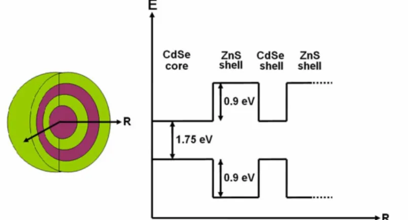
Fig. 1. Schematic of an onion-like (CdSe)ZnS/CdSe/ZnS heteronanocrystal structure (with violet regions representing CdSe and green regions representing ZnS) along with the corresponding radial energy diagram (not drawn to scale).
2. Theoretical background
Nanocrystals such as (CdSe)ZnS (core)shell quantum dots typically reveal almost spherical, slightly elongated shapes according to the high-resolution transmission electron microscopy (HRTEM) measurements [25]. In our theoretical formalism, for simplicity we consider a spherically symmetric heteronanocrystal structure to separate its wavefunctions into the radial and angular parts, as presented in Eq. (1) in spherical coordinates ( , , )rθ φ . In Eq. (1),
( ) nl
R r is the radial wavefunction, Ylm( , )θ φ is the spherical harmonic, n is the principal quantum number, and l and m are the angular momentum numbers. Here, in the case that a particular eigenenergy (Enl) of the heteronanocrystal is higher than the potential in its qth layer, i.e., Enl>Vq, then the corresponding radial wavefunction Rnl q, ( )r (the radial wavefunction in the qth layer) for the associated energy state Enl is a linear combination of spherical Bessel and Neumann functions. On the other hand, in the case of Enl<Vq, the solution Rnl q, ( )r is a linear combination of Hankel functions.
For our theoretical analysis, we apply effective mass approximation, which is a widely-used method in quantum mechanical analysis. It has been previously shown that the effective mass approximation works well even for few-monolayer quantum structures [26]. Thus, the effective mass approximation has been used for a number of spherical nanocrystal heterostructures [17,27-30]. Also, in our theoretical analysis as a valid approach, we solve for the energy levels (eigenvalues) and wavefunctions (eigenfunctions) of the CdSe-ZnS heteronanocrystal using effective mass approximation. The associated wavefunction solutions must then satisfy the continuity condition at all boundaries of the heteronanocrystal layers (i.e., the boundary conditions) as in Eqs. (2) and (3).
)
,
(
)
(
)
,
,
(
θ
φ
θ
φ
ψ
nlmr
=
R
nlr
Y
lm (1)q q nlq r r r r q nl
r
R
r
R
,(
)
|
==
, +1(
)
|
= (2) q q r r q nl q r r q nl qdr
r
dR
m
dr
r
dR
m
= + + ==
1
(
)
)
(
1
, 1 * 1 , * (3)In our (CdSe)ZnS/CdSe/ZnS (core)shell/shell/shell hetero-NC, there are four layers and three boundaries, as schematically shown in Fig. 1. Because Rnl( )r has to be regular at r = 0 and has to converge to zero when r→ ∞, there are six unknown coefficients for its basis functions, and there are six equalities coming from Eqs. 2 and 3 applied at its three boundaries. To find nontrivial solution, the determinant of these coefficients should be zero, i.e., Dl=Dl(Enl)=0. Restricting our consideration to only S-symmetry states (with zero angular momentum) [29,30], the wavefunction depends on the radial part Rn,l=0(r) that makes l=0 and
m=0, and thus the wavefunction becomes only dependent on r. By using the normalization
condition forRnl( )r , all the coefficients of the basis functions are then determined.
After solving for energy levels and wavefunctions, we calculate the exciton binding energy due to the Coulomb interaction between the electron and hole pair using the first-order perturbation theory [30]. The binding energy is given in Eq. (4), where e and h subscripts refer to electron and hole, respectively, and ε is the high frequency dielectric constant. After expanding the 1/|re-rh| term in Eq. (4) in the form of spherical harmonics and integrating over the angular coordinates, the binding energy is written as in Eq. (5), where εr is the mean dielectric constant.
∫∫
−
−
=
)
,
(
|
|
)
(
)
(
)
(
)
(
* * h e h e h h e e h h e e h e cr
r
r
r
r
r
r
r
dr
dr
E
ε
ψ
ψ
ψ
ψ
(4)∫∫
−
=
)
,
(
)
,
max(
|
)
(
|
|
)
(
|
4
2 2 2 2 0 2 h e r h e h h e e h e h e cr
r
r
r
r
R
r
R
r
r
dr
dr
e
E
ε
πε
(5)The material parameters used in our quantum mechanical analysis is summarized in Table 1 and the corresponding potential profile is shown in Fig. 1 [15,31]. When a single monolayer of CdSe (or ZnS, by the same token) is added surrounding an existing spherical dot, the expansion of the resulting dot occurs in all three directions (x,y,z). However, (CdSe)ZnS/CdSe/ZnS hetero-NC is made of a wurtzite structure, in which the lattice constants in x and y directions are equal and the lattice constant in z direction is different from the others. Therefore, we calculate the mean of lattice constants in x-y plane and z direction. As a result, we take 1 monolayer (ML) CdSe to be 0.56 nm thick [32] and 1 ML ZnS to be 0.49 nm thick [33], given in Table 1. For our simulations we use a CdSe core of 2.75 nm radius and subsequently add alternative layers of ZnS and CdSe shells, each with changing thickness from 1 to 3 monolayers around this CdSe core. To find bounded solutions, we complete the onion-like structure with an infinitely thick ZnS barrier.
Table 1. Material parameters for CdSe and ZnS.
Material me* mh* Monolayer
thickness (nm) Band discontinuity (eV)
CdSe 0.13 0.45 0.56 -
3. Analysis of electronic structure in multi-layered heteronanocrystals
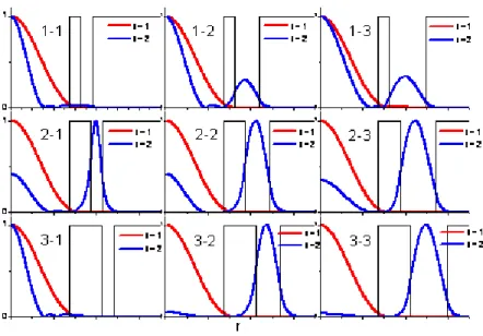
Beginning with the analysis of 2S states in (CdSe)ZnS/CdSe/ZnS heteronanocrystals, Fig. 2 shows the probability distribution of the electron |ψe,200(r)|2and the hole
2 200 , ( )|
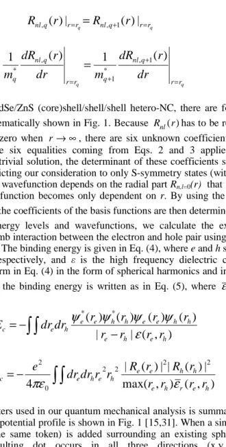
|ψh r (normalized with respect to the peak for easy visual inspection) at the first excited states n=2. Here again note that these (CdSe)ZnS/CdSe/ZnS heteronanocrystals are analyzed with the thickness of their inner ZnS and CdSe shells varied from 1 ML to 3 MLs, while their CdSe core is kept fixed and the outmost ZnS shell is taken infinitely thick. At these n=2 energy states, we observe that the carrier distribution is tuned between the localization regimes of type-1 (with electrons and holes primarily residing in the same layer) and type-2 (with electrons and holes primarily residing in different layers) by changing the thickness of the shell layers. In the cases of 1 ML ZnS and 1 ML CdSe shells (indicated as 1-1 in our notation in Fig. 2), 1 ML ZnS and 2 ML CdSe shells (1-2), 1 ML ZnS and 3 ML CdSe shells (1-3), and 2 ML ZnS and 1 ML CdSe shells (2-1), both the electron and hole mainly reside in the CdSe core, with their distribution maxima overlapping in the center of the core, showing type-1-like localization. However, for the cases of 2 ML ZnS and 3 ML CdSe shells (2-3) and 3 ML ZnS and 1 ML CdSe shells (3-1), the distribution maxima of the electron and the hole are clearly separated, with one type of the carrier mainly residing in the CdSe core while the other residing mainly in the CdSe shell, showing type-2-like localization. In the cases of 2 ML ZnS and 2 ML CdSe shells (2-2), 3 ML ZnS and 2 ML CdSe shells (3-2), and 3 ML ZnS and 3 ML CdSe shells (3-3), both the electron and hole mainly reside in the CdSe shell, which shows type-1-like carrier localization again. Here it is worth noting that the electron and hole localize in the CdSe shell rather than in the CdSe core in the final type-1-like localization cases. As a result, by varying the thickness of ZnS and CdSe shells, we observe that it is possible to tune the carrier localization from type-1 to type-2 regime and from type-2 back to type-1 regime again.
Fig 2. 2S relative probability distribution of electron |ψe,200(r)|2 (in blue) and hole 2
200 , ( )|
|ψh r (in red) for n=2, l=0, m=0 states (with their peaks normalized to 1 for easy visualization) across the radial potential profile V(r) (in black) of the entire heteronanocrystal. On each plot, the thicknesses of the inner ZnS shell (the first shell) and the CdSe shell (the second shell) in monolayers (e.g., x ML ZnS and y ML CdSe) are labeled as a pair (in the convention of x-y) in our notation. (For instance, 1-3 indicates (CdSe)ZnS/CdSe/ZnS heteronanocrystal with a 1-monolayer ZnS inner shell and a 3-monolayer CdSe shell).
At n=2 energy states, both the electron and hole tunnel to the CdSe shell, as shown in Fig. 2. This situation plays a critical role in multi-color emission, as will be explained in the next section. Although in conventional mono-color emitting (CdSe)ZnS (core)shell NCs a 3 ML ZnS barrier provides sufficient isolation for carrier confinement [14], this may not be sufficient for full carrier localization at n=2 in (CdSe)ZnS/CdSe/ZnS heteronanocrystals. When ZnS thickness CdSe shell thicknesses are varied, at n=2 energy level the hole tends to localize mainly either in the CdSe core or in the CdSe shell layer. When ZnS barrier thickness is fixed to 1 ML, as the CdSe shell thickness is increased, the hole tunnels further more and more toward the CdSe shell, and when the CdSe shell thickness is increased to 3 MLs, the hole localization in the shell becomes as distinguishable as it is in the core. Similar behavior is also observed for 2 ML ZnS shell with increasing CdSe shell thickness. For example, in the case of 2 ML ZnS and 3 ML CdSe shells (2-3), the probability of the hole residing in the CdSe shell is higher than in the CdSe core. Similarly, when we have 3 ML ZnS and 1 ML CdSe shells (3-1), the hole is localized in the core, but as we increase CdSe shell thickness to 2 MLs (3-2) and then further to 3 MLs (3-3), the probability distribution of the hole in the core eventually decays almost to zero and the hole localization in the CdSe shell dominates.
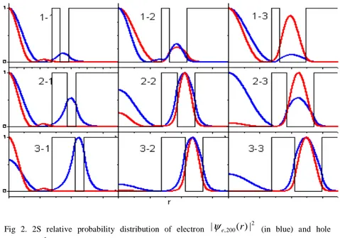
Analyzing 1S states in (CdSe)ZnS/CdSe/ZnS heteronanocrystals, we observe that both electron and hole are mainly localized in the core at the ground state (n=1) as shown in Fig. 3. One of the important characteristics of the mono-color emitting (CdSe)ZnS (core)shell NCs is that they confine electrons and holes in the core with strong localization, leading to high quantum efficiencies (up to 66%) [34]. In hetero-NCs at the ground state, ZnS makes a good barrier for both the electron and hole as well. Only, in the case of 1 ML ZnS and 3 ML CdSe shells (1-3), the electron tunnels with a relatively low probability to the CdSe shell. Nevertheless, we conclude that the ZnS barrier in general provides significant isolation for both carriers in (CdSe)ZnS/CdSe/ZnS hetero-NCs at the ground state, like (CdSe)ZnS (core)shell NCs.
Fig. 3. 1S relative probability distribution of electron |ψe,100(r)|2(in blue) and hole 2
100 , ( )|
|ψh r (in red) for n=1, l=0, m=0 states (with their peaks normalized to 1 for easy visualization) across the radial potential profile V(r) (in black) of the entire heteronanocrystal. On each plot, the thicknesses of the inner ZnS shell (the first shell) and the CdSe shell (the second shell) in monolayers (e.g., x ML ZnS and y ML CdSe) are labeled as a pair (in the convention of x-y) in our notation. (For instance, 1-3 indicates (CdSe)ZnS/CdSe/ZnS heteronanocrystal with a 1-monolayer ZnS shell and a 3-monolayer CdSe shell).
4. Analysis of optical properties and multi-color emission in multi-layered heteronanocrystals
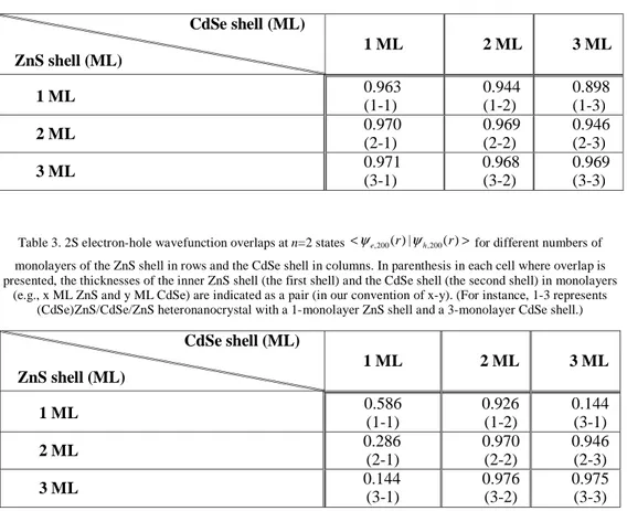
In multi-color emitting heteronanocrystals, lower-energy photons originate from the CdSe core and higher-energy photons from the CdSe shell. Battaglia, et al., demonstrated multi-color emitting onion-like structures by changing ZnS and CdSe shells from 1 ML to 3 MLs [23]. However, some structures surprisingly did not exhibit multi-color emission, instead they featured only mono-color emission from CdSe core through 1S transition. To achieve multi-color emission from such hetero-NCs, according to our simulation we find out that lower-energy excitons should be localized in the CdSe core at n=1 states, and higher-lower-energy excitons should be localized in the CdSe shell at n=2 states. In addition, the overlaps of these electron-hole wavefunctions for the corresponding optical transitions between the associated energy states should be relatively high (because the optical transition probability is directly proportional to the electron and hole wavefunction overlap [31]). For (CdSe)ZnS/CdSe/ZnS heteronanocrystal, the electron-hole spatial overlaps calculated for n=1 are relatively high (near to 1) as summarized in Table 2 and the associated excitons are mainly localized in the CdSe core at n=1 as shown in Fig. 4, which is the same situation for mono-color emitting (CdSe)ZnS (core)shell nanocrystals.
Fig. 4. The electron-hole spatial wavefunction multiplication (exciton) distribution
| ) ( ) (
|ψe,n00rψh,n00 r for n=1 (in red) and n=2 (in blue), l=0, m=0 states (with their peaks
normalized to 1 for easy visualization) across the radial potential profile V(r) (in black) of the entire heteronanocrystal. On each plot, the thicknesses of the inner ZnS shell (the first shell) and the CdSe shell (the second shell) in monolayers (e.g., x ML ZnS and y ML CdSe) are labeled as a pair (in the convention of x-y) in our notation. (For instance, 1-3 indicates (CdSe)ZnS/CdSe/ZnS heteronanocrystal with a 1-monolayer ZnS shell and a 3-monolayer CdSe shell).
Table 2. 1S electron-hole wavefunction overlaps <ψe,100(r)|ψh,100(r)> for different numbers of monolayers of the
ZnS shell in rows and the CdSe shell in columns at n=1 states. In parenthesis in each cell where overlap is presented, the thicknesses of the inner ZnS shell (the first shell) and the CdSe shell (the second shell) in monolayers (e.g., x ML
ZnS and y ML CdSe) are indicated as a pair (in our notation of x-y.) (For instance, 1-3 represents (CdSe)ZnS/CdSe/ZnS heteronanocrystal with a 1-monolayer ZnS shell and a 3-monolayer of CdSe shell).
CdSe shell (ML) ZnS shell (ML) 1 ML 2 ML 3 ML 1 ML 0.963 (1-1) 0.944 (1-2) 0.898 (1-3) 2 ML 0.970 (2-1) 0.969 (2-2) 0.946 (2-3) 3 ML 0.971 (3-1) 0.968 (3-2) 0.969 (3-3)
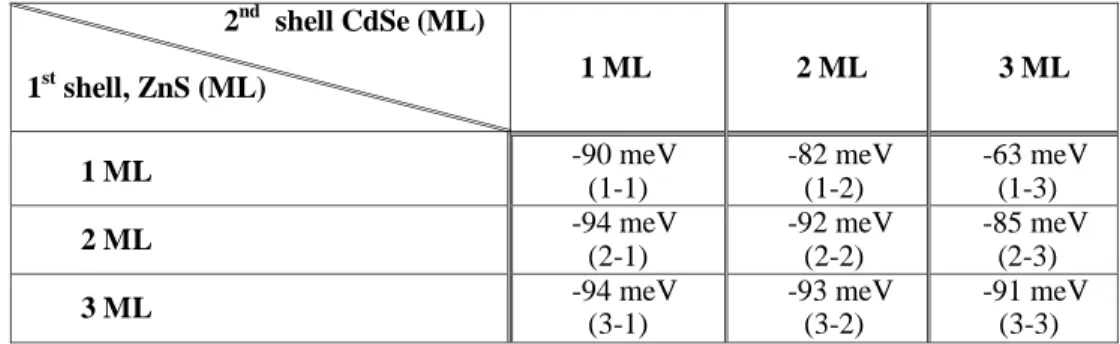
Table 3. 2S electron-hole wavefunction overlaps at n=2 states <ψe,200(r)|ψh,200(r)> for different numbers of monolayers of the ZnS shell in rows and the CdSe shell in columns. In parenthesis in each cell where overlap is presented, the thicknesses of the inner ZnS shell (the first shell) and the CdSe shell (the second shell) in monolayers
(e.g., x ML ZnS and y ML CdSe) are indicated as a pair (in our convention of x-y). (For instance, 1-3 represents (CdSe)ZnS/CdSe/ZnS heteronanocrystal with a 1-monolayer ZnS shell and a 3-monolayer CdSe shell.)
CdSe shell (ML) ZnS shell (ML) 1 ML 2 ML 3 ML 1 ML 0.586 (1-1) 0.926 (1-2) 0.144 (3-1) 2 ML 0.286 (2-1) 0.970 (2-2) 0.946 (2-3) 3 ML 0.144 (3-1) 0.976 (3-2) 0.975 (3-3) Battaglia, et al., did not obtain multi-emission specifically for the cases of 1 ML ZnS and 1 ML CdSe shells (1-1), 1 ML ZnS and 2 ML CdSe shells (1-2), 1 ML ZnS and 3 ML CdSe shells (1-3), 2 ML ZnS and 1 ML CdSe shells (2-1), and 3 ML ZnS and 1 ML CdSe shells (3-1) [23]. For all of these cases at n=2, both the electron and hole are confined in the core rather than in the shell, as demonstrated in Fig. 4. We consider that the excitons possibly relax from n=2 state to n=1 state before they recombine. Thus, the emission occurs only between 1S states. This situation is in agreement with the timescales of the associated processes. In this material system [35], the spontaneous emission lifetime is typically tens of nanoseconds (around 20 ns) [3] and the intersubband relaxation time is typically hundreds of femtoseconds (around 100 fs) [36]. Thus, relaxation to lower energy states takes place statistically before radiative recombination. Additionally, according to Battaglia, et al., and Sapra, et al., in (CdSe)ZnS/CdSe/ZnS multi-layered heteronanocrystals, there is energy transfer (with uncertainty whether Förster or Dexter type of energy transfer) [23,24]. However, to the best of our knowledge, the energy transfer timescale has not been determined for these particular structures to date, although some time-resolved measurements have been reported [23,24]. On the other hand, the cases of 2 ML ZnS and 2 ML CdSe shells (2-2), 2 ML ZnS and 3 ML CdSe shells (2-3), 3 ML ZnS and 2 ML CdSe shells (3-2), and 3 ML ZnS and 3 ML CdSe shells (3-3) exhibit radiative 2S transitions, as also Battaglia, et al., experimentally observed [23]. In these cases, the excitons are localized in the CdSe shell for n=2 states as demonstrated in Fig. 4, and the associated overlaps are relatively high (near to 1) as shown in Table 3.
Heteronanocrystal structures achieving multi-color emission exhibit that their electrons and holes are mainly localized in the core for n=1 states and in the shell for n=2 states. In this case we consider that the intersubband transition of carriers at n=2 states, which are primarily localized in the shell, to n=1 states is weak due to the low probability distribution of electrons and holes in the shell at n=1 states. This situation facilitates spontaneous emission to take place between n=2 states in the shell, leading to multi-color emission. We also compare the overlaps for 1S and 2S transitions with the experimentally measured relative peak luminescences [23]. For example, the overlap in the case of 2 ML ZnS and 3 ML CdSe shells (2-3) is higher than the overlap in the case of 2 ML ZnS and 2 ML CdSe shells (2-2) for 2S transition, and the luminescence from n=2 states of (2-3) is theoretically predicted to be relatively higher than (2-2), as also previously experimentally shown. We observe similar confirmation of our theoretical predictions with the experimental measurements also for the cases of 3 ML ZnS and 3 ML CdSe shells (3-3) and 3 ML ZnS and 2 ML CdSe shells (3-2).
Examining the energy levels of (CdSe)ZnS/CdSe/ZnS heteronanocrystals we observe that both the core and shell energy levels change when the thicknesses of the ZnS and CdSe shells are changed, as Battaglia, et al., also experimentally demonstrated [23]. For 1S transitions, we find similar levels of energy change in our theoretical work with respect to the case of mere CdSe core as shown in Fig. 5(a), excluding the binding energy due to the Coulomb interaction. For 1 ML ZnS, as the CdSe shell thickness is increased, the photoluminescence shifts with an increasing slope towards red. The increase of the PL peak shift for the case of 1 ML ZnS is larger than for the cases of 2 ML ZnS and 3 ML ZnS because, in the 3 ML ZnS shell case, the electron and hole wavefunctions slightly leak into the CdSe shell. In 3 ML ZnS shell, the change in PL is almost zero because 3 ML ZnS shell is a good barrier for carrier confinement for n=1 states. These calculated results match the experimental results very well within a precision of 2-5 nm range. When we take the Coulomb interaction into account to investigate the change of the core CdSe emission as shown in Fig. 5(b), although the difference between the measured and calculated results increases to a range of 1-11 nm, we observe the blue shift for 3 ML ZnS, as was also observed in the experiment [23]. In the hetero-NC, in each case, the binding energy is smaller in magnitude than the only core case (-95 meV), as shown in Table 4. Therefore, because of the weaker Coulomb interaction in hetero-NCs, the red shift due to the exciton confinement is reduced. In other words, as a result of the Coulomb interaction, in the hetero-NC structure, there exists a relative blue shift with respect to the mere CdSe core case. The binding energies between 2S transitions for different ZnS and CdSe shells (by taking into account the Coulomb interaction) are summarized in Table 5. 0 1 2 3 0 2 4 6 8 10 PL pe ak s h if t ( n m ) CdSe layers 1 ML ZnS 2 ML ZnS 3 ML ZnS 0 1 2 3 -1.5 -1.0 -0.5 0.0 0.5 1.0 1.5 P L peak s h ift ( n m) CdSe layer 1 ML ZnS 2 ML ZnS 3 ML ZnS (a) (b) Fig. 5. Theoretical energy level shifts of (CdSe)ZnS/CdSe/ZnS heteronanocrystal for different
thicknesses of the ZnS shell and the CdSe shell with respect to the mere core CdSe NC (a) without and (b) with taking the Coulomb interaction into account.
Table 4. Exciton binding energy due to the Coulomb interaction at n=1 states. 2nd shell CdSe (ML) 1st shell, ZnS (ML) 1 ML 2 ML 3 ML 1 ML -90 meV (1-1) -82 meV (1-2) -63 meV (1-3) 2 ML -94 meV (2-1) -92 meV (2-2) -85 meV (2-3) 3 ML -94 meV (3-1) -93 meV (3-2) -91 meV (3-3) For 2S transition energies, we observe good agreement between our theoretically calculated data and the experimentally measured data in [23]. In the cases of 1 ML ZnS and 1 ML CdSe shells (1-1), 1 ML ZnS and 2 ML CdSe shells (1-2), 1 ML ZnS and 3 ML CdSe shells (1-3), 2 ML ZnS and 1 ML CdSe shells (2-1), and 3 ML ZnS and 1 ML CdSe shells (3-1), we theoretically explained in the previous sections that these samples should not have luminescence for 2S. In Table 6, we present the calculated and measured optical emission wavelengths for 2S transitions. For example, particularly for the case of 3 ML ZnS and 3 ML CdSe shells (3-3), we calculate the PL wavelength to be 578 nm, whereas the experimentally measured PL peak is approximately at 575 nm. Also, in the cases of 2 ML ZnS and 3 ML CdSe shells (2-3), and 3 ML ZnS and 2 ML CdSe shells (3-2), we observe similar agreement between the experimental and theoretical results.
Table 5. Exciton binding energy due to the Coulomb interaction at n=2 states. 2nd shell, CdSe (ML) 1st shell, ZnS (ML) 1 ML 2 ML 3 ML 1 ML -30 meV (1-1) -23 meV (1-2) -21 meV (1-3) 2 ML -9 meV (2-1) -23 meV (2-2) -24 meV (2-3) 3 ML -2 meV (3-1) -21 meV (3-2) -23 meV (3-3)
Table 6. Comparison of our theoretical PL peaks and the experimental PL peaks for different CdSe and ZnS thicknesses for 2S transitions.
1 ML 2 ML 3 ML
2nd shell, CdSe (ML)
1st shell, ZnS (ML)
Theo. Exp.a Theo. Exp. a Theo. Exp. a
1 ML - (1-1) - (1-1) - (1-2) - (1-2) - (1-3) - (1-3) 2 ML - (2-1) - (2-1) 520 nm (2-2) 550 nm (2-2) 576 nm (2-3) 580 nm (2-3) 3 ML - (3-1) - (3-1) 520 nm (3-2) 535 nm (3-2) 578 nm (3-3) 575 nm (3-3) a Reference [23].
We further investigate the possibility of triple-color emission from multi-layered hetero-NCs based on CdSe-ZnS material system. According to our theoretical investigations given any possible combination of shell thickness, we do not observe any case that confines excitons for n=1 state in the core, for n=2 state in the first CdSe shell, and for n=3 state in the second CdSe shell, disabling potential triple-color emission. For instance, we examine a (CdSe)ZnS/CdSe/ZnS/CdSe/ZnS (core)shell/shell/shell/shell/shell heterostructure by adding ZnS shell (as the third shell) and CdSe shell (as the fourth shell) of various thicknesses surrounding the 3-shell hetero-NC with 3 ML ZnS and 3 ML CdSe shells (3-3) that achieves dual-color emission. Even for the case of 3 ML of the third shell and 3 ML of the fourth shell, we do not observe triple-color emission because electrons at n=2 and n=3 states are confined together either in the second shell or in the fourth shell depending on the fifth shell thickness. Thus, this situation prevents the formation of localized excitons for n=2 and n=3 states separately in different layers. Therefore, according to our investigations, we do not encounter a case that would potentially provide triple-color emission from a 5-shell hetero-NC in CdSe-ZnS material system.
5. Conclusion
In conclusion, we quantum mechanically investigated the electronic properties and the resulting optical properties of multi-layered (CdSe)ZnS/CdSe/ZnS (core)shell/shell/shell nanocrystals and verified our theoretical results with the previous experimental measurements. We showed that the carrier localization at the first excited state is tuned from type-1-like to type-2-like localization and from type-2-like to type-1-like localization back again, by varying the first shell (ZnS) and the second shell (CdSe) thicknesses. We revealed that ZnS barrier used in the first shell (even for 3 monolayers) does not necessarily fully confine electron and hole at n=2 state, though providing significant electron and hole isolation at n=1 state. We showed that the distinct spatial localization of excitons at n=1 and n=2 is key to achieve multi-color emission, in addition to the requirement of relatively high electron-hole wavefunction overlaps. Furthermore, we investigated the possibility of triple-color emission from multi-layered hetero-NCs based on CdSe-ZnS material system and we did not observe any case that would potentially achieve triple-color emission.
Acknowledgments
The authors thank Dr. M. O. Oktel and Dr. S. Sapra for valuable discussions. This work is supported by EU-PHOREMOST NoE 511616 and Marie Curie European Reintegration Grant MOON 021391 and TUBITAK under the Project No. 106E020, 104E114, 107E088, 107E297, 105E065, and 105E066. Also, HVD acknowledges additional support from the Turkish Academy of Sciences Distinguished Young Scientist Award (TUBA GEBIP) and European Science Foundation (ESF) European Young Investigator Award (EURYI) Programs.