FABRICATION AND CHARACTERIZATION
OF ZINC OXIDE BASED SURFACE
ACOUSTIC WAVE DEVICES
A THESIS
SUBMITTED TO MATERIALS SCIENCE AND NANOTECHNOLOGY PROGRAM
OF THE GRADUATE SCHOOL OF ENGINEERING AND SCIENCE OF BILKENT UNIVERSITY
IN PARTIAL FULFILLMENT OF THE REQUIREMENTS FOR THE DEGREE OF
MASTER OF SCIENCE
By
Mehmet Alican Noyan
August, 2013
ii
I certify that I have read this thesis and that in my opinion it is fully adequate, in scope and in quality, as a thesis for the degree of Master of Science.
Assist. Prof. Dr. Necmi Bıyıklı (Advisor)
I certify that I have read this thesis and that in my opinion it is fully adequate, in scope and in quality, as a thesis for the degree of Master of Science.
Assist. Prof. Dr. Çağlar Elbüken
I certify that I have read this thesis and that in my opinion it is fully adequate, in scope and in quality, as a thesis for the degree of Master of Science.
Assoc. Prof. Dr. H. Emrah Ünalan
Approved for the Graduate School of Engineering and Science:
Prof. Dr. Levent Onural Director of Graduate School
iii
ABSTRACT
FABRICATION AND CHARACTERIZATION OF ZINC
OXIDE BASED SURFACE ACOUSTIC WAVE
DEVICES
Mehmet Alican Noyan
M.S. in Materials Science and Nanotechnology Advisor: Assist. Prof. Dr. Necmi Bıyıklı
August, 2013
Surface acoustic wave (SAW) devices, as applied to today’s technology, were first described in 1965. Since then, these devices were applied to a wide variety of fields. Bandpass filter is their most common application, which is an important component in consumer products such as televisions and mobile phones. SAW devices can also be utilized as chemical and biological sensors. Driving force behind the development of SAW sensors is their small size, high sensitivity, reliability, and durability.
This thesis presents the development and characterization of ZnO/Si based SAW devices. ZnO thin films with c-axis orientation were deposited using rf-magnetron sputtering. Effect of post deposition annealing on the structure of ZnO and on the SAW device performance was studied. It was found that annealing ZnO above 600oC is detrimental for SAW device performance.
Surface roughness of ZnO increases as the annealing temperature increases. In literature, roughness increase is presented as one of the reasons behind device breakdown. This work shows that roughness is not the primary cause for the breakdown. In addition, effect of SiO2 interlayer insertion between ZnO/Si
structure on the device performance was examined together with the effect of ZnO thickness.
Keywords: Surface acoustic wave (SAW) device, Zinc oxide (ZnO), Sputtering,
iv
ÖZET
ÇİNKO OKSİT TEMELLİ YÜZEY AKUSTİK DALGA
AYGITLARININ GELİŞTİRİLMESİ VE
NİTELENDİRİLMESİ
Mehmet Alican Noyan
Malzeme Bilimi ve Nanoteknoloji, Yüksek Lisans Tez Yöneticisi: Yrd. Doç. Dr. Necmi Bıyıklı
Ağustos, 2013
Bugün bildiğimiz anlamda kullanılan yüzey akustik dalga (SAW) aygıtları, ilk olarak 1965’te tanıtıldı. Televizyon ve cep telefonu gibi tüketici ürünlerinde kullanılan band geçiren filtreler bu cihazların en yaygın kullanım alanıdır. SAW aygıtlar ayrıca kimyasal ve biyolojik algılayıcı olarak da kullanılabilir. SAW algılayıcı geliştirmenin arkasında yatan temel neden bu cihazların küçük boyutlu, yüksek hassasiyette ve dayanıklı olmalarıdır.
Bu tez ZnO/Si yapısına dayalı SAW aygıtının geliştirilmesini ve nitelendirilmesini sunmaktadır. C-eksen yönelimli ZnO ince filmler, sıçratma yöntemi ile kaplanmıştır. Kaplama sonrasında uygulanan tavlamanın ZnO yapısına ve SAW aygıt başarımına etkisi detaylı bir şekilde incelenmiştir. 600oC üzerindeki sıcaklıklarda tavlamanın SAW aygıtı olumsuz etkilediği tespit edilmiştir. ZnO’in yüzey pürüzlülüğü tavlama sıcaklığı arttıkça artmaktadır. Kaynaklar, pürüzlülük artışını aygıtın tavlama sıcaklığı artışına dayalı bozunumunun nedenlerinden biri olarak vermektedir. Bu çalışma ise bozunumun yüzey pürüzlülüğünden kaynaklanmadığını göstermektedir. Tavlamanın aygıt başarımı üzerindeki etkisine ek olarak, ZnO/Si yapısının arasına SiO2 eklenmesinin ve ZnO kalınlığının da aygıt başarımına etkileri
incelenmiştir.
Anahtar kelimeler: Yüzey akustik dalga (SAW) aygıtları, Çinko oksit (ZnO),
v
vi
Acknowledgements
I would like to express my appreciation to my supervisor Assist. Prof. Dr. Necmi Bıyıklı for his guidance, encouragement and advice throughout the development of this work. I would also like to thank Assist. Prof. Dr. Çağlar Elbüken and Assoc. Prof. Dr. H. Emrah Ünalan for being in my thesis committee and sharing their useful comments.
I am grateful to İnci Dönmez for her endless support even in hard times, to Engin Çağatay for teaching me almost everything I know in the cleanroom, and to Çağla Özgit-Akgün for sharing her profound knowledge with me. Not forgetting my friends who always been there: Levent, Deniz, Feyza, Fatih, Adem, Sami, Enver, Furkan, Burak, Ayşe, Elif, Pelin, Gamze, Enes and Tahsin. I would particularly like to thank UNAM engineers Semih Yaşar, Fikret Piri and Mustafa Güler. Furthermore, I would like to thank Elif Aydoğdu, Amir Ghobadi and Çağrı Çetintepe for their help during network analyzer measurements.
I would like to express my appreciation to my uncle Prof. Dr. İsmail Cevdet Noyan for his invaluable contributions to the content of the thesis.
Finally, yet importantly, I would like to express my heartfelt thanks to my beloved family, Aslı, Aytül and Turgut Noyan for their endless support.
vii
Contents
Chapter 1 Introduction ... 1
1.1 Motivation ... 2
1.2 Objectives... 2
1.3 Organization of the Thesis ... 3
Chapter 2 Theoretical Background and Literature Overview ... 4
2.1 Theory of Piezoelectricity ... 4
2.1.1 History... 4
2.1.2 Crystal Geometry ... 6
2.1.3 Tensors ... 10
2.1.4 Piezoelectricity... 13
2.1.5 Derivation of the piezoelectric moduli for the point group 6mm ... 17
2.2 Theory of SAW devices ... 27
2.2.1 Theory of Operation... 27
2.2.2 Surface Waves... 31
2.2.3 Parameters Affecting Wave Propagation... 33
2.2.4 Measurement... 34
2.3 Literature Overview ... 34
Chapter 3 Experimental Details... 37
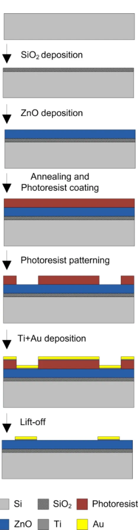
3.1 Device Fabrication ... 37
3.1.1 Substrate and Surface Preparation ... 38
3.1.2 SiO2 Deposition Using RF Magnetron Sputtering... 38
3.1.3 ZnO Deposition Using RF Magnetron Sputtering ... 39
3.1.4 Post-deposition Annealing of ZnO ... 40
3.1.5 Formation of Interdigitated Transducers (IDT) ... 41
3.1.5.1 Photolithography ... 41
3.1.5.2 Deposition of Titanium and Gold... 44
3.1.5.3 Lift-off ... 45
3.2 Characterization Methods ... 47
3.2.1 Methods Used for ZnO Characterization ... 47
3.2.1.1 X-Ray Diffraction... 47
viii
3.2.1.3 Scanning Electron Microscopy... 51
3.2.1.4 Transmission Electron Microscopy ... 51
3.2.1.5 Spectroscopic Ellipsometry ... 52
3.2.1.6 Atomic Force Microscopy ... 53
3.2.2 SAW Device Characterization ... 55
Chapter 4 Results and Discussion... 59
4.1 Optimization and Characterization of ZnO... 59
4.1.1 Optimization of Deposition Parameters... 59
4.1.1.1 Deposition Temperature ... 60
4.1.1.2 Deposition Power ... 62
4.1.1.3 Chamber Pressure ... 63
4.1.2 Characterization of ZnO... 65
4.1.3 Post-deposition Annealing ... 69
4.2 Characterization of SAW Devices ... 76
4.2.1 Effect of Annealing... 76
4.2.2 Effect of SiO2 Interlayer ... 81
4.2.3 Effect of Film Thickness... 82
Chapter 5 Conclusions and Future Directions ... 83
ix
List of Figures
Figure 1.1: A surface acoustic wave device. ... 1
Figure 2.1: Unit cell which can be defined with three vectors or six scalars [10]. ... 7
Figure 2.2: 14 Bravais lattices [10]. ... 7
Figure 2.3: Operation of symmetry elements mirror plane and rotation axes [10]. ... 8
Figure 2.4: (a) Atomic arrangement of a hexagonal close packed structure, circles represent atoms (b) Hexagonal lattice with two atoms per lattice point. Atoms marked with x are atoms shown in (a) [10]. ... 9
Figure 2.5: Crystal structure of CsCl(a) [10], ZnO(b) [11]... 9
Figure 2.6: Transformation of axes. Angle between and is shown. ... 11
Figure 2.7: Ion positions in a quartz lattice with and without external stress [12]. ... 14
Figure 2.8: Symmetry elements of the point group 6mm. A six-fold rotation axis, two mirror planes. x1 and x2 axes are shown. x3 axis is parallel to the 6-fold rotation axis, with the direction out of the page. ... 17
Figure 2.9: Transformation of axes by the mirror plane shown by the straight line. ... 18
Figure 2.10: Transformation of axes by the second mirror plane. ... 20
Figure 2.11: Transformation of axes due to 6-fold rotation axis... 22
Figure 2.12: Crystal structure and surface free energies for three different planes of ZnO [11]... 26
Figure 2.13: Interdigital transducer function on a piezoelectric material [15]... 27
Figure 2.14: Basic working principle of a SAW device. Edge view [15]... 28
Figure 2.15: Surface acoustic wave delay line with interdigitated transducer dimensions... 29
Figure 2.16: (a) Longitudinal, (b) Transverse wave [16]. ... 31
Figure 2.17: Shear vertical and shear horizontal vibration types [16]. ... 31
x
Figure 3.1: VAKSIS NanoD – 4S Magnetron Sputtering system which was used
for SiO2, ZnO, Ti and Au thin film depositions. ... 39
Figure 3.2: ATV-Unitherm (RTA SRO-704) rapid thermal annealing (RTA) system... 40
Figure 3.3: (a) Spinning of HMDS and AZ5214E were done in Laurell spinner system. (b) Precision hot plates where soft and hard-bake steps were performed. ... 42
Figure 3.4: Heidelberg Instruments DWL-66 Laser Mask Writer used for photomask production. ... 43
Figure 3.5: EVG 620 mask aligner used for the exposure of photoresist-coated wafers. ... 44
Figure 3.6: Microfabrication steps of SAW devices used in this work... 46
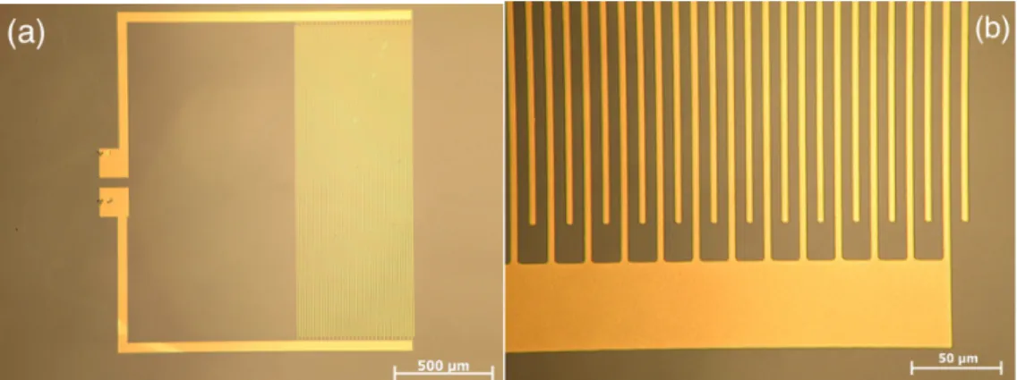
Figure 3.7: Optical microscope images of the final device showing gold electrodes over ZnO. (a) One of the interdigital transducers. (b) Finger pairs. . 47
Figure 3.8: Schematic representation of Bragg’s law. ... 48
Figure 3.9: PANalytical X'Pert PRO Multi-Purpose X-Ray Diffractometer used for the XRD measurements ... 49
Figure 3.10: Schematic representation of the basic components of X-ray photoelectron spectroscopy. ... 50
Figure 3.11: Thermo Scientific K-Alpha X-Ray photoelectron spectroscopy system... 50
Figure 3.12: Nova-NanoSem scanning electron microscope. ... 51
Figure 3.13. FEI Tecnai G2 F30 transmission electron microscope. ... 52
Figure 3.14: J.A. Woolam Co. V-VASE spectroscopic ellipsometer. ... 53
Figure 3.15: Schematic representation of how tip movements are detected typically in AFM. ... 54
Figure 3.16: PSIA XE-100E atomic force microscope used for the morphological characterization of ZnO films. ... 54
Figure 3.17: Schematic two-port network... 56
Figure 3.18: A scheme showing calibration steps. The order is not important.. 57
xi
Figure 3.20: Schematic illustration of the measurement... 58 Figure 3.21: Actual measurement setup showing network analyzer (E5071C) and the probe station (a), RF probes and the device under test can be seen in (b).
... 58 Figure 4.1: Radial scans of the 0002 reflections for the films deposited at three different temperatures... 61 Figure 4.2: Radial scans of the 0002 reflections for the films deposited under three different rf power values. ... 62 Figure 4.3: Radial scans of the 0002 reflections for film deposited at different chamber pressures. ... 64 Figure 4.4: SEM image of the (a) surface and (b) cross section of the sputtered 402 nm thick ZnO on Si wafer. ... 65 Figure 4.5: TEM image of the ZnO cross section. SiO2 is the native oxide of the
silicon wafer while Pt is the holder coated during sample preparation... 66 Figure 4.6: XPS depth profile analysis results of the ZnO thin film over silicon wafer showing the uniform composition throughout the bulk film... 67 Figure 4.7: (a) Zn 2p and (b) O 1s high resolution XPS spectra of the optimized ZnO thin film after 300 s of Ar etch... 68 Figure 4.8: AFM image of sputtered ZnO over silicon wafer... 68 Figure 4.9: Fitting data of the ZnO film using Cauchy dispersion function to obtain thickness and refractive index values... 69 Figure 4.10: Radial scans of the 0002 reflections for the as-deposited and annealed films... 70 Figure 4.11: RMS surface roughness values of the films annealed at different temperatures. Error values are smaller than the height of the data points... 72 Figure 4.12: Refractive index of the films annealed at different temperatures. Error values are smaller than the height of the data points. ... 73 Figure 4.13: SEM image of the ZnO surface annealed at (a) 600°C and (b) 1000oC. ... 74 Figure 4.14: RMS surface roughness vs. Annealing temperature graph for annealing durations 5 and 30 min... 75
xii
Figure 4.15: Radial scans of the 0002 reflections for the films annealed at 1000°C for 5 and 30 min. ... 75 Figure 4.16: Response of the SAW devices utilizing ZnO annealed at (a) 400°C for 30 min, (b) 600°C for 5 min, (c) 600°C for 30 min, (d) 800°C for 5 min, (e) 800°C for 30 min, (f) 1000°C for 5 min and (g) 1000°C for 30 min. ... 78 Figure 4.17: Insertion loss vs. frequency response of the devices utilizing ZnO annealed at 600°C for 5 and 30 min. ... 80 Figure 4.18: Effect of SiO2 addition on SAW device response. ... 81
Figure 4.19: Insertion loss vs frequency response of the devices utilizing 1560 and 1890 nm thick ZnO... 82
xiii
List of Tables
Table 2.1: Restrictions imposed on by the mirror plane whose normal is
parallel to ... 20
Table 2.2: Restrictions imposed on piezoelectric moduli coefficients... 21
Table 2.3: Resulting after restrictions in Table 2.2 are applied... 21
Table 2.4: after the restrictions imposed by both mirror planes... 21
Table 2.5: Coefficients of the piezoelectric moduli after restrictions imposed by the transformations due to symmetry elements 6, m, m... 23
Table 2.6 SAW device application areas after Hickernell [25]... 35
Table 3.1: Optimized Sputtering Parameters for ZnO Deposition... 40
Table 3.2: Sputtering parameters for titanium and gold... 45
Table 4.1: Integrated intensity values with respect to different deposition temperatures. ... 61
Table 4.2: Integrated intensities per unit thickness for different RF power values. ... 63
Table 4.3: Integrated intensities per unit thickness for the films deposited using three different chamber pressures... 64
Table 4.4: ZnO deposition recipe determined for the VAKSIS RF magnetron sputtering system... 65
Table 4.5: Integrated intensity per unit thickness and full width at half maximum values according to annealing temperatures... 70
1
Chapter 1
Introduction
Surface acoustic wave (SAW) devices are composed of two interdigital transducers (IDTs) fabricated on a piezoelectric material (Figure 1.1). This material can be a piezoelectric substrate or a piezoelectric thin-film over a non-piezoelectric substrate. Piezoelectric materials deform under the application of electric fields (E-fields) and form E-fields under the application of stress. A given electrical signal to the input IDT transformed to mechanical deformation in the crystal due to piezoelectricity. If this electrical signal is oscillating, then the deformation would be oscillating. Oscillating deformation causes surface acoustic waves in the solid. When this wave reaches the output IDT, it is converted back to the electrical signal. IDT dimensions allow a signal with a specific frequency to pass.
2
These devices are used as the frequency filters in wireless communication systems. Perturbance of the wave at the surface between the IDTs would cause attenuation and phase shifting of the electrical signal obtained at the output IDT. Inspecting the relation between the cause of the perturbance and the change in the signal resulted in the development of SAW sensors.
1.1 Motivation
SAW devices have wide range of application areas. In electronic circuitry, SAW devices can be used as oscillators, filters and transformers. Some important advantages of these devices are their small size and weight, durable structure and easy production.
SAW devices are also employed as sensors due to their unique advantages. First important advantage is the confinement of SAW energy in the surface of the device which enables the production of very high sensitive devices. In addition, dimensions of these devices are small hence they can be easily integrated into various platforms.
1.2 Objectives
In this work, SAW devices based on ZnO over silicon wafer were fabricated. The essential purpose of this work was to investigate the parameters affecting SAW device operation and optimize them for improved performance. Effects of post-deposition annealing on ZnO structure and SAW device operation were investigated in detail. In addition, influence of deposition parameters on the crystal structure of ZnO was studied. Afterwards, addition of SiO2 interlayer
between ZnO and the substrate was reported. Finally, the effect of ZnO thickness on the device performance was analyzed.
3
1.3 Organization of the Thesis
This part briefly explains the organization of the thesis. In Chapter 2, theory of piezoelectricity and SAW devices are presented. This part is crucial for understanding and improving device performance. Same chapter also includes a brief overview of the SAW sensor literature. In Chapter 3, fabrication of the SAW device is explained in detail. It is followed by the introduction of the experimental methods used to characterize the piezoelectric film and the SAW device. Results of these characterizations are presented and discussed in Chapter 4. Thesis concludes with Chapter 5 which gives a summary of the work presented in this thesis and possible future directions of study.
4
Chapter 2
Theoretical Background and
Literature Overview
In this chapter, a brief history on piezoelectricity and main concepts of the piezoelectric theory will be introduced. Afterwards, ZnO will be examined in terms of its piezoelectric properties. In addition, theory of surface acoustic wave (SAW) devices will be discussed including the operation principles, surface waves, parameters affecting wave propagation and the measurement methods. Chapter will end with a brief literature overview on SAW devices.
2.1 Theory of Piezoelectricity
2.1.1 History
Piezoelectricity literally means electricity caused by pressure where 'piezo' means press in Greek. From a scientific point of view, piezoelectricity is defined by Cady [1] as follows, “electric polarization produced by mechanical strain in crystals belonging to certain classes, the polarization being proportional to the strain and changing sign with it.” Actually this is the definition of direct piezoelectric effect. When subject to electrical polarization, a piezoelectric crystal becomes mechanically strained. This is called the converse piezoelectric
5
effect. The direct piezoelectric effect is named as 'direct' only because it is realized before the converse piezoelectric effect.
Curie brothers, Pierre and Jacques Curie, have been credited for the discovery of piezoelectricity in 1880, although piezoelectricity was observed before their work. Here, it is convenient to quote the introduction paragraphs of their paper [1], [2] in which they announced their discovery, in translation:
“Those crystals having one or more axes whose ends are unlike, that is to say hemihedral crystals with oblique faces, have the special physical property of giving rise to two electric poles of opposite signs at the extremities of these axes when they are subjected to a change in temperature: this is the phenomenon known under the name of pyroelectricity.
We have found a new method for the development of polar electricity in these same crystals, consisting in subjecting them to variations in pressure along their hemihedral axes”
Wilhelm Gottlieb Hankel, a senior experimental physicist, dealed with this new effect and could not find a general correlation between this new phenomenon and pyroelectricity; hence, Hankel claimed it is an independent phenomenon and proposed the name 'piezoelectricity' for this new effect [3]. In 1881, Gabriel Lippmann examined piezoelectricity in terms of thermodynamic principles and concluded that there should be a reverse effect [4]. Later that year Curie brothers verified the statement [5].
In 1890s, Lord Kelvin constructed the theory of piezoelectricity [6] based on thermodynamic grounds and piezoelectric formulation was handled rigorously by Woldemar Voigt [7].
6
It took some time for piezoelectricity to find a practical application. In 1917, Paul Langevin [8], doctoral student of Pierre Curie, showed that quartz plates could be used to emit and receive sound waves under water. Langevin developed the first sonar (abbreviation of sound navigation and ranging) using this principle. This development awakened the interest for piezoelectric devices and led to the research and development of new piezoelectric materials and new applications. Today, piezoelectricity is utilized in a wide variety of applications such as radio transmission, filter technology, nano-positioning, measurement of pressure, velocity and acceleration, gas sensors, biological sensors etc.
2.1.2 Crystal Geometry
Understanding crystals is indispensable for understanding piezoelectricity. Piezoelectricity depends on the crystal structure of the material and amorphous materials do not possess piezoelectricity (except some polymers [9]).
A crystal is a solid composed of atoms, ions or molecules in which they are arranged in an ordered pattern in three dimensions. In order to the study the periodicity of crystals, lattices are used. Lattice is a three dimensional array of points. All of these points have the same surrounding with each other and they are called as lattice points. It is critical to remember that atom sites and lattice points are different entities.
Unit cells are the cells which can be used to define the whole lattice. Vectors a, b, c (or six scalars a, b, c, α, β, γ) define a unit cell entirely (Figure 2.1). A unit cell defines the entire lattice.
7
Figure 2.1: Unit cell which can be defined with three vectors or six scalars [10].
Depending on the magnitude and direction of these vectors, units cells of various shapes can occur. There are only seven different kind of crystal systems and only fourteen different point lattices which fulfill the requirement of a point lattice. These 14 point lattices are called Bravais lattices (Figure 2.2).
8
Crystals possess symmetry and it is a way to define crystals. If an operation performed on the crystal leaves it indistinguishable from its previous state this operation is called as symmetry operation. Elements used to define these operations are called symmetry elements. There are four symmetry operations: reflection, rotation, inversion and roto-inversion. For instance mirror plane (designated as ‘m’) is the symmetry element used to define reflection. Rotation axes define the operation rotation (Figure 2.3). If a body has n-fold rotation axis (represented as ‘n’), a rotation of 360o/n about that axis will bring it into coincidence with itself. A lattice can possess more than one symmetry element. Point groups define the symmetry elements possessed by a lattice. There are 32 point groups.
Figure 2.3: Operation of symmetry elements mirror plane and rotation axes [10].
Until now, lattices were discussed instead of actual crystals. Discussion on actual crsytals should start with stating the relation between lattice points in a Bravais lattice and atoms (or ions or molecules) of a crystal. For each lattice point, there is one or more atom in the crystal related to it. Hence actual crystals possess the symmetry elements of their Bravais lattice.
It is possible to have one atom on one lattice site which is simple to imagine. Copper, for example, has face-centered cubic structure. Each copper atom sits onto a lattice point. There are also crystals in which more than one
9
atom is related to one lattice point. Zinc, for example, has a hexagonal closed packed (HCP) structure. There are two atoms per unit cell. (Figure 2.4(a)). HCP structure belongs to hexagonal Bravais lattice. Each lattice point is related to two Zn atoms (Figure 2.4(b)). Atoms shown in Figure 2.4(a) are marked with x in Figure 2.4(b).
Figure 2.4: (a) Atomic arrangement of a hexagonal close packed structure, circles represent atoms (b) Hexagonal lattice with two atoms per lattice point. Atoms marked with x are atoms shown in (a) [10].
There are also compounds to consider. They have more than one type of atom therefore additional rules are applied. First, same kind of atoms form a crystal structure. For example, structure shown in Figure 2.5(a) is simple cubic not body centered cubic. Secondly, atoms of same kind should possess the same symmetry, independent of each other, with the entire crystal (Figure 2.5(b)).
10
2.1.3 Tensors
Piezoelectricity is not a scalar quantity, it is direction dependent. Therefore tensors should be used to define piezoelectric effect. Tensors are multi-dimensional array of numbers. It is different from a matrix in the sense that a tensor has a physical meaning, it describes a physical quantity. It can be said that tensor is a matrix with attitude. Rank of a tensor can be defined as the number of directions needed to define a tensor. The number of indices of a tensor coefficient is also equal to the rank of the tensor. Scalar quantities like temperature and density are tensors of zero-rank. Vectors are tensors of first-rank.
Coefficients of a tensor are determined according to the choice of axes. If axes change, coefficients would also change. However, both tensors would represent the same physical quantity. For the reasons revealed later in this chapter, it is important to understand how transformations should be performed, therefore it will be worked out with examples.
As a first example, it will be shown how a first rank tensor, a vector, components transform when the axes are transformed. Consider , , axes were transformed into new set of axes , , .
11
Figure 2.6: Transformation of axes. Angle between and is shown.
€
Cij is the cosine of the angle between
€
xi' and
€
xj. It is called a direction cosine and the array of values are represented by the matrix
€
Cij
( )
. Direction cosines of with respect to , , are , , .Suppose a vector e with components , , . Component of e on new axes would be , , . will be determined by the projection of components
, , on it. Hence:
Similarly,
12
This is the transformation law for a vector, a first-rank tensor. Reverse tranformation law, that is the transformation from the new axes back to the old axes, would be defined as:
Now consider we have two vectors a and b. For the set of axes , , ,
they are related to each other with the second rank tensor , with the equation
a b (e.g. the relation between electric field (E-field) which is a vector and
current which is also a vector, is defined as conductivity which is a second rank tensor). If we define new set of axes , , , components of the vectors will change from , to , . We now wonder , the relation between and , in terms of . This can be derived by writing in terms of , in terms of ,
and in terms of . € ai' = Cijaj € aj = Tjkbk € bk = Clkbl '
Combining to reach the relation between and ,
Then transformed tensor would be,
€ Til' = CijTjkClk or more clearly, € TAB ' = CAaCBbTab
is the transformation law for the second-rank tensor. Reverse transformation would be given by
13
Piezoelectricity is a third rank tensor, therefore transformation law for a third rank tensor will be shown as a last derivation. For a third rank tensor, description of the relation between a vector P and a second rank tensor σ is,
€
Pi = dijkσjk
Transformation law for the third rank tensor, , can be derived with similar arguments used to reach the law for the second rank tensor:
Combining to reach the relation between and ,
€ Pi' = CijPj = Cijdjklσkl = CijdjklCxkCylσxy ' € Pi' = dixy' σxy' Transformation law for the third-rank tensor is,
€
dixy'
= CijCxkCyldjkl
2.1.4 Piezoelectricity
When a stress is applied to a crystal, electric moment occurs and under an electric field, a crystal strains. These two effects are called piezoelectricity, former being the direct one and the latter being the reverse one. Figure 2.7 simply shows how mechanical forces could unbalance dipole moments, resulting in polarization.
14
Figure 2.7: Ion positions in a quartz lattice with and without external stress [12].
Quartz is the one of the most widely known piezoelectric material. If a uniaxial stress (tensile or compressive) is applied along one of the 2-fold rotation axis of the quartz crystal, an electric moment will develop on the same axis.
P is the dipole moment and σ is the stress. Linear relation between them, d, is called piezoelectric modulus. Polarization changes direction according to the direction of stress (tensile or compressive). Stress is a second-rank tensor and polarization is a vector. 27 coefficients are needed to define the relation between them. Hence, piezoelectric moduli dijk is a third-rank tensor with 27 coefficients,
15 In general form (using Einstein notation),
€
Pi = dijkσjk
The piezoelectric moduli are equal for the direct and converse piezoelectric effects therefore if direct effect is formulated as
€
Pi = dijkσjk, converse effect can
be written as,
€
εjk = dijkEi
where E-field, , applied to a crystal produces strain, , in the crystal. The piezoelectric moduli in direct and converse effects being equal are predicted by Lippmann and proved experimentally by Curie brothers.
There are piezoelectric constants other than d, such as e, g, and h. To calculate the E-field due to applied stress, one should first calculate polarization ( ) then E-field can be calculated using ( ) where is relative permittivity. To define indirect relation such as this, e, g, and h are used.
, ,
For the relation between strain and polarization, , ,
where Y is Young’s Modulus. Last coefficient, , defines the relation between E-field and strain,
16
There is one last important property left to define piezoelectricity thoroughly. That is electromechanical coupling coefficient, . It defines the efficiency of transduction. If , for example, this means 20% of the electric energy applied will be available as mechanical energy, and vice versa. Electromechanical coupling coefficient is related to piezoelectric constants as [12],
Elements of symmetry in a crystal reduce the number of independent variables in the piezoelectric moduli. If axes are transformed by one of the symmetry element present in the crystal, dijk should remain the same because
crystal would be the same after the transformation. It is stated in the postulate known as Neumann’s Principle.
‘The symmetry elements of any physical property of a crystal must include the symmetry elements of the point group of the crystal’.
Among 32 crystal classes, 20 of them exhibit piezoelectricity. These are the non-centrosymmetric point groups except 432.
Piezoelectric crsytal classes are: 1, 2, m, 222, mm2, 4, 4, 422, 4mm, 42m, 3, 32, 3m, 6, 6, 622, 6mm, 62m, 23, 43m.
To illustrate the effect of symmetry on the piezoelectricity, piezoelectric moduli for the 6mm point group will be derived in the next section. It is the point group possessed by ZnO.
17
2.1.5 Derivation of the piezoelectric moduli for the point group
6mm
Piezoelectric moduli will be transformed with the application of each symmetry element. The moduli after transformation should be equal to the moduli before transformation due to Neumann’s principle. Figure 2.8 shows the symmetry elements of the point group 6mm. Although there are six mirror planes, only two of them are distinct. Consider one of the planes shown by the dotted line, with the application of 6-fold rotation axis on that plane other two planes shown with the dotted lines can be obtained therefore they are not distinct. Two distinct planes are shown by dotted and straight lines.
Figure 2.8: Symmetry elements of the point group 6mm. A six-fold rotation
axis, two mirror planes. x1 and x2 axes are shown. x3 axis is parallel to the
6-fold rotation axis, with the direction out of the page.
Firstly, restrictions imposed by the mirror plane whose normal is parallel to will be examined (shown by the straight line in Fig. 2.8). Figure 2.9 shows how this mirror plane transforms the axes.
18
Figure 2.9: Transformation of axes by the mirror plane shown by the straight line.
Now direction cosines for this transformation should be determined, remembering is the cosine of the angle between and . For example is the cosine of the angle between and , which is . Whole matrix should be,
Only non-zero direction cosines are
€
C
11=1
,€
C
22= −1
,€
C
33= 1
. Transformation law for the third-rank tensor is,Coefficients of the moduli should be equal to after this transformation. Let us start with considering first coefficient,
€ d111 ' = C1IC1JC1KdIJK € d111' = C11C11C11d111+ C11C11C12d112+ C11C11C13d113+ C11C12C11d121+ ... All components following the first component contain or which is zero. Therefore is the only non-zero component, becomes,
19 €
d111'
= d111 this means can take any value, there is no restriction imposed by the mirror plane (Fig. 2.9) on the value of this coefficient. Consider the second coefficient,
Implementing the same approach used in . The only non-zero term is hence,
€
d112' = −d112
then, and must be equal to zero in order to satisfy both Neumann’s principle (
€
d112 '
= d112) and the restriction ( ) imposed by the transformation according to the mirror plane in Figure 2.9.
There are 27 components, it would be tiresome to do this calculation for each of them. This derivation can be performed more easily. It should be realized that and
€
C
xx=1,−1
for the direction cosine of the transformation due to mirror plane in Figure 2.9.Consider again, the transformation law . If
, , then direction cosines will be either one or zero. Examine the case for the . Therefore and there will be no restriction for the coefficients with the indices , , . If only one of the i, j, k is 2 then . is zero for coefficients with only one indice is equal to 2. Examine the case for the above. If two of the indices i, j, k are equal to 2 than (since
€
(−1) × (−1) = 1). There is no restriction. If, finally, than . Therefore .
20
Now restrictions imposed by the mirror plane could be tabulated in order to understand the result more clearly (Table 2.1).
Table 2.1: Restrictions imposed on by the mirror plane whose normal
is parallel to jk i 11 12 13 21 22 23 31 32 33 1 0 0 0 0 2 0 0 0 0 0 3 0 0 0 0
Now let us consider the restrictions imposed by the other mirror plane (Figure 2.10).
Figure 2.10: Transformation of axes by the second mirror plane.
21
Using the similar arguments used to derive the restrictions imposed by the mirror plane in Figure 2.9, restrictions for the mirror plane in Figure 2.10 can be listed as follows,
Table 2.2: Restrictions imposed on piezoelectric moduli coefficients.
, , No restriction
One indice equal to 1
Two indices equal to 1 No restriction
The result of the restrictions can be tabulated as follows (Table 2.3),
Table 2.3: Resulting after the restrictions in Table 2.2 are applied.
jk
i 11 12 13 21 22 23 31 32 33
1 0 0 0 0 0
2 0 0 0 0
3 0 0 0 0
Combining both restrictions would yield (Table 2.4),
Table 2.4: after the restrictions imposed by both mirror planes.
jk
i 11 12 13 21 22 23 31 32 33
1 0 0 0 0 0 0 0
2 0 0 0 0 0 0 0
22
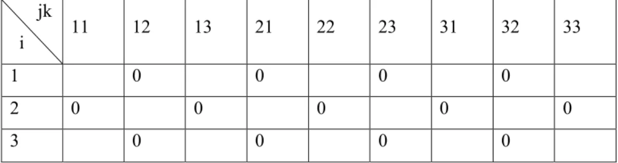
Here, it should be noted that and are equal because the stess tensor is symmetric ( ). In general , and there is one symmetry operation left to study and five independent coefficients, , , , and .
Figure 2.11 shows the transformation of axes with the application of 6-fold rotation axis (
€
360o/6 = 60o rotation), parallel to .
Figure 2.11: Transformation of axes due to 6-fold rotation axis.
For this transformation, direction cosines are given as,
For the first component ,
Since is non-zero only when K=3,
23 Solving together with the equation
€
d113' = d113,
For the ,
For the last coefficient ,
Since is either zero or one,
€
d333' = d333
Combining all restrictions would give all coefficients for the 6mm point group (Table 2.5),
Table 2.5: Coefficients of the piezoelectric moduli after restrictions imposed by the transformations due to symmetry elements 6, m, m.
jk
i 11 12 13 21 22 23 31 32 33
1 0 0 0 0 0 0 0
2 0 0 0 0 0 0 0
3 0 0 0 0 0 0
In conclusion, there are only three independent coefficients , , in a piezoelectric moduli of a crystal belonging to the point group 6mm.
24 € dijk = 0 0 d113 0 0 0 d113 0 0 0 0 0 0 0 d113 0 d113 0 d311 0 0 0 0 0 0 0 d333 ⎡ ⎣ ⎢ ⎢ ⎢ ⎤ ⎦ ⎥ ⎥ ⎥
There is a convention used to reduce the tensor. Stress tensor is a symmetric tensor (i.e ) therefore there are six independent components instead of nine. Reduced notation for the stress tensor is as follows,
For this reduction,
Here coefficient 2 creates a problem for representing this equation in general form. This can be overcomed as follows. Right now and
€
d
i23+ d
i32= 2d
i4 By defining, € di23+ di32 = di4 di13+ di31= di5 di12+ di21= di6€
P
i= d
i1σ
1+ d
i2σ
2+ d
i3σ
3+ d
i4σ
4+ d
i5σ
5+ d
i6σ
6 € Pi = dijσjAccording to this reduction, reduced piezoelectric module for the 6mm point group would be,
25
2.1.5 Piezoelectricity of ZnO
ZnO is a wide-band gap semiconductor and has a variety of applications in today’s technology. Possible crystal structures of ZnO are wurtzite, zinc blende and rocksalt. Wurtzite is the thermodynamically stable phase at ambient conditions. Zinc-blende ZnO can be grown on cubic substrates while the rocksalt structure could be grown in high pressures.
In the wurtzite structure, each Zn is surrounded by four O atoms where Zn atom resides in the middle of a tetrahedron and O atoms sit at the corners of the tetrahedron, and vice versa. This arrangement is typical of covalent bonding but ZnO also possesses ionic character. Ionicity of ZnO is at the boundary between ionic and covalent semiconductor [13]. Without this ionic character ZnO would not exhibit piezoelectricity since ionicity is required to form electric moment.
There are wide variety of deposition techniques to deposit thin film ZnO. These include sputtering, sol-gel process, pulsed laser deposition, atomic layer deposition, molecular beam epitaxy, metal-organic vapor deposition, and plasma enhanced chemical vapor deposition [14]. ZnO thin film reported in this work is deposited using rf-magnetron sputtering. Sputtering is a simple technique, in which required orientation for piezoelectricity can be obtained at room temperature independent of the substrate used. (0001) plane, which is the basal plane of ZnO, has the lowest surface free energy (Figure 2.12). Therefore, sputtered ZnO has a (0001) preferred orientation. Basal planes are parallel to the surface of the film [11].
26
Figure 2.12: Crystal structure and surface free energies for three different planes of ZnO [11].
As demonstrated in section 2.1.5, piezoelectric moduli of ZnO has three independent coefficients , , . These are [12],
€ dij = 0 0 0 0 −12 0 0 0 0 −12 0 0 −4.7 −4.7 12.0 0 0 0 ⎡ ⎣ ⎢ ⎢ ⎢ ⎤ ⎦ ⎥ ⎥ ⎥ pC N
Remembering the converse effect,
€
εjk = dijkEi and , ,
, it should be noted that only E-fields in the direction of [100] and [001] produce strain in the ZnO crystal.
27
2.2 Theory of SAW devices
2.2.1 Theory of Operation
Basic working principle behind the SAW devices is conversion of electromagnetic (EM) waves into acoustic waves and converting acoustic waves back into the electromagnetic waves. Interdigital transducers (IDTs) are used for both of the conversions. In the former conversion, reverse piezoelectric effect is utilized whereas latter conversion uses direct piezoelectric effect. As illustrated in Figure 2.13, when a potential difference is applied between the fingers of an IDT, E-field lines pass from the piezoelectric substrate.
Figure 2.13: Interdigital transducer function on a piezoelectric material [15].
Since the material is piezoelectric, E-field causes mechanical deformation which is known as reverse piezoelectric effect, assuming that the material and its crystallographic orientation is convenient for this conversion (Section 2.1). If the applied E-field is oscillating, then resulting mechanical deformation will also be oscillating. Oscillating mechanical fields cause mechanical waves in the solid. They travel perpendicular to the long edges of the IDT finger in both directions. Mechanical waves deform the crystal as they travel and due to direct piezoelectric effect, there is a potential field accompanying the mechanical
28
wave. If this wave reaches another IDT, a potential difference will occur within the IDT finger pairs due to direct piezoelectric effect. This is how a SAW device basically works (Figure 2.14).
Figure 2.14: Basic working principle of a SAW device. Edge view [15].
There are two main configurations for SAW devices. First one is the SAW delay line and the other one is the SAW resonator. SAW delay line is the device described in Figure 2.14. Figure 2.15 illustrates top view of a SAW delay line. There are two IDTs at the same surface apart from each other with a propagation length of L. Input IDT converts EM signal to acoustic wave, it travels to the output IDT and converts back to an EM signal. It is called as a delay line because acoustic wave travels the distance L much slower than an EM signal. Therefore, the signal is delayed between two IDTs. In the second configuration, one or two IDTs are used to construct a resonant cavity. In this configuration, generated acoustic wave reflects back from the ends of the substrate and starts to resonate which can be detected using the generating IDT or another one. Devices fabricated in this work are SAW delay lines.
29
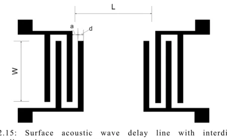
Figure 2.15: Surface acoustic wave delay line with interdigitated transducer dimensions.
IDT dimensions (Figure 2.15) determine the wavelength of the acoustic waves. Each IDT pair generates acoustic waves. When a generated wave in one pair meets with the other wave generated in the next finger pair, they interfere. If the distance between finger pair centers is an integer multiple of the wavelength of the wave, then constructive interference occurs, the other wavelengths destruct each other. Therefore, the SAW wavelength is defined as
and the central frequency is defined as,
where subscript 0 stands for the unperturbed values. is the acoustic wave velocity and it depends on the substrate material, orientation of the substrate and the type of the wave generated. When the propagation of the SAW is perturbed somehow, velocity of the wave changes. This perturbance can be measured as the frequency shift. Measurement of this perturbance is the principle behind SAW sensors.
Frequency of the acoustic waves ranges from few MHz to GHz. Sizes of the devices depend on the frequencies. Smaller devices are needed for higher frequencies (as d decreases, wavelength decreases which in turn increases the frequency). The limit for smaller devices is the fabrication technologies
30
available. For lower frequencies, devices should enlarge and this is limited by the substrate size.
Dimensions of the IDTs are given in Figure 2.15. L is the propagation length. Increasing L results in an increase in attenuation whereas a decrease in noise levels. Numbers of finger pairs, , determine the frequencies around the central frequency, which is called as bandwidth ( ). Increasing finger pairs decreases bandwidth because frequencies near the central frequency would survive if there is less finger pairs, as the finger pairs increase the constructive interference increases for the near-central frequencies. is the finger spacing and is the finger width. Metallization ratio is defined as the ratio of the area coated with metal to the electrode area, which is given by the formula . In this work, metallization ratio is fixed to 0.5 (i.e.
€
d = a). Final dimension, W, is
the overlap of fingers which is termed as aperture.
It is important to note that, other than using a piezoelectric substrate (e.g. quartz, LiNbO3) for the fabrication of SAW devices, a piezoelectric thin film
(e.g. ZnO, AlN) over a non-piezoelectric substrate (e.g. Si) could be utilized. The advantage of using a piezoelectric thin film is its applicability to variety of substrates. Using Si as the substrate, SAW device can be implemented to electronic circuits. In this study, ZnO was used as the piezoelectric film and silicon was used as the substrate.
As explained before, E-field in the directions [100] and [001] are the only directions to produce strains in the ZnO wurtzite crystals and sputtered ZnO grows with its c-axis (i.e. [001] direction) perpendicular to the surface. IDTs parallel to the ZnO surface will create curved E-fields with components perpendicular and parallel to the surface (Figure 2.13). Perpendicular E-field components are in the [001] direction since c-axis is also perpendicular to the surface. Therefore this configuration leads to ZnO based SAW devices. Thus it can be deduced that improving c-axis orientation of ZnO will improve
31
piezoelectricity and this will improve the device performance by increasing the efficiency of transduction
2.2.2 Surface Waves
In this part, nature of the surface acoustic waves will be stated. There are three fundamental particle motions constituting wave motion. These are linear, circular and elliptical motions. Longitudinal (2.16(a)) waves and the transverse (2.16(b)) waves are the two basic wave types.
Figure 2.16: (a) Longitudinal, (b) Transverse wave [16].
In transverse (shear) waves, particle motion and wave propagation is perpendicular to each other whereas in longitudinal (compressional) waves, particle motion and the wave propagation are parallel. In a transverse wave, direction of the particle motion determines the polarization of the wave and propagation direction of the wave determines the energy transfer direction.
For shear waves propagation along a surface, there exist two important vibration types which are shear vertical and shear horizontal (Figure 2.17).
32
Surface acoustic waves were first described by Lord Rayleigh in 1885 [17]. The particle motion in Rayleigh waves is elliptical. The wave has both compressional and shear components. Elliptic motion is in the plane perpendicular to the surface. Wave propagation is parallel to the elliptical motion and the surface plane. Major axis of the ellipse is perpendicular to the surface. Particle motion is counter-clockwise when the wave moves from left to right. Rayleigh waves attenuate exponentially going from surface to the bulk of the substrate, and its energy is confined to one wavelength of thickness.
Figure 2.18: A schematic illustration of Rayleigh Wave [18].
Consider a Rayleigh wave with and a piezoelectric substrate with a thickness of . Since Rayleigh wave travels in the top , thickness of the substrate is not very important in this case. But in a layered structure such as ZnO-Si, ZnO thickness can vary from few hundreds of nanometers to few tens of microns therefore it affects wave propagation. For this case, normalized thickness (i.e. ) should be considered. It can be defined as where h is the layer thickness and is the wavelength. Within the range
Rayleigh wave is the fundamental wave mode [14, 16, 19].
Above this range, a second order Rayleigh wave, called Sezawa wave, appears along with the Rayleigh wave. Below this range, other acoustic modes such as plate waves occur. The devices studied in this work are within the range , therefore the acoustic mode utilized in these devices is Rayleigh wave.
33
2.2.3 Parameters Affecting Wave Propagation
It is important to understand the phenomena perturbing wave motion in order to interpret the device response correctly.
Temperature has considerable effect on wave propagation mainly because many material properties (material constants) are temperature dependent. The amount of perturbation depends on the material and the crystal orientation it possesses. This dependency also led to temperature sensors based on SAW devices [20].
Pressure is another important factor affecting SAWs. SAWs produce waves in the gas when they are in contact with it mainly due to its shear horizontal component. This causes attenuation in the SAWs and it is more prominent as the pressure increases. Pressure sensors were shown by Scherr et al. [21]. Liquid loading is another type of pressure. Measurements in liquid (e.g. SAW biosensor) causes liquid loading on the surface. Rayleigh wave seriously attenuates in this case, therefore a device utilizing a wave mode without shear horizontal component should be used.
As stated in Section 2.2.1, there is a potential field following the propagation of SAW. This potential field could be perturbed by an E-field applied close to it. This in turn would affect the propagation of the SAW. In addition, presence of a conducting or semi-conducting film on top of the substrate surface would perturb the wave due to electrical properties of the film apart from the mass loading.
One last property to consider is the surface roughness. Surface defects cause scattering of the SAWs. This results in attenuation of the wave. Additionally, this scattering could result in acoustic mode conversion [16, 22].
34
2.2.4 Measurement
The measurement of these devices is mainly done through network analyzers. Attenuation and phase shifting of the SAWs can be deduced from the scattering parameter S21, which is the ratio of input and transmitted power. Since this
transfer is done by acoustic waves, it is a measure of its characteristics. There are also oscillator based measurements. In this method, SAW device is used as a frequency controlling element of an oscillator circuit. For the measurements of SAW devices fabricated in this work, network analyzer is used.
2.3 Literature Overview
First effective SAW device appeared in 1965 [23]. White and Voltmer introduced IDTs for direct generation and detection of SAWs. Before this discovery, generation and detection were done using mechanical coupling of a transducer to the device body which was ineffective. Abundant ideas followed this discovery. Frequency and time domain devices to augment signal processing ability of microwave systems were developed first. Today, SAW market is a large, where the global market value of SAW devices reached nearly $1.1 billion in 2011 and it is expected to reach $1.8 billion by 2016 [24]. The main application field of these devices is telecommunications where it is used as a bandpass filter in RF range (e.g. in mobile phones). Still, SAW devices have wide variety of applications from wine tasting to satellite systems (Table 2.6).
35
Table 2.6 SAW device application areas after Hickernell [25]
Telecommunications:
Cellular, personal communication systems and networks, cordless, mobile, pagers, wireless local loops, base stations, global satellite.
Data Communications:
Digital radio, wireless local area networks, handheld data terminals, global positioning systems.
Video Applications:
Television, cable television, video cassette recorders, high definition TV, direct broadcast satellite TV, interactive TV, cable modems, video games.
Automotive and Home:
Remote keyless entry, theft deterrent systems, alarms, remote meter readings, home appliances, audio equipment, identification tags.
Military & Space:
Electronic warfare, signal intelligence, battlefield
communications, avionics, fuzing, orbital and deep space satellite systems, surveillance system, missiles.
Other Markets:
Sensors, test equipment, high frequency clocks, computers, commercial avionics.
SAW devices fabricated in this work are intended to be used in sensing applications. Therefore, review of the SAW literature will focus mainly on sensor applications. The first SAW sensor was developed by Wohltjen et al. in 1979 [26]. They showed that surface molecules affect the wave propagation. Interactions were measured by the changes in amplitude and phase shift. They found that amplitude response is proportional to the pressure of the gas in the environment, and showed that response is proportional to (molecular weight)1/2. In 1980, Fertsch, White and Muller showed that detection of organic vapors using polyvinyl chloride films on the delay line surface is possible [27]. In 1981, Bryant, Lee and Vetelino compared bulk acoustic wave (BAW) and SAW sensors for SO2 and found that SAW sensor is able to detect SO2 less than 100
ppb, which means SAW device is an order of magnitude more sensitive than BAW sensor [28].
36
Some of the vapor recognition materials and target vapors pairs reported in the literature are polyepichlorohydrine-toluene [29], polyisobutylene-octane [30], palladium-hydrogen [31] and zinc oxide-ammonia [32]. In addition, spray-coated composite polyethylenimine (PEI) with SiO2/Si nanoparticles was used
for the sensing of ethanol, and laser-deposited PEI was used for the sensing of methanol [33].
Biosensor applications of SAW devices were developed later, mainly because biosensors are usually required to work in liquids and Rayleigh waves attenuate seriously under liquid loading as explained in Section 2.2. In order to overcome this problem, device configurations utilizing acoustic modes such as surface transverse waves [34], shear horizontal SAWs [35] and Love Waves [36] were used.
In order to convert a SAW device to a biosensor, a layer responsive to the specific analyte is deposited onto the delay line surface. When the layer engages to the analyte, mass of the layer will increase and this will be reflected as a change in the acoustic wave. Using this method SAW biosensors were demonstrated for the detection of DNA [37], bacteria [38] and protein [39].
Devices fabricated in this work, layered ZnO-SiO2-Si SAW devices
utilizing Rayleigh waves, are first described in 1982 [40] and worked out until now [41-45].
37
Chapter 3
Experimental Details
In this chapter, firstly, SAW device fabrication process is described including the explanation of microfabrication steps, equipments used and process parameters in detail. Subsequently, methods and equipments used for the characterization of material properties of ZnO and properties of the SAW device are introduced.
3.1 Device Fabrication
This section provides a detailed explanation of the microfabrication process flow leading to the fabrication of SAW devices. All of the microfabrication processes were performed at UNAM Cleanroom Facility (UCF), in class 100 and class 1000 lab spaces.
38
3.1.1 Substrate and Surface Preparation
500 µm thick Si (100) wafer pieces were used as the substrate for the SAW devices. Wafers were cut into pieces using a diamond scriber. Surface cleanliness of the Si wafer pieces is important for the repeatability of materials and device characteristics as well as for good film adhesion onto the substrate surface. To eliminate particles and organic impurities on the surface, a three-stage substrate cleaning procedure was performed. First, samples were sonicated in acetone ((CH3)2CO) for 10 min to remove organic contamination. Afterwards,
samples were sonicated in isopropyl alcohol ((CH3)2CHOH) for 10 min.
Samples were rinsed with deionized (DI) water and dried with nitrogen gun. The final step was to bake pieces at 120oC for 5 min on a hot plate in order to
eliminate any possible adsorbed water vapor remainings. Coating should be performed as soon as possible after cooling the sample to room temperature to avoid re-adsorption of water vapor from the environment.
3.1.2 SiO2 Deposition Using RF Magnetron Sputtering
VAKSIS NanoD – 4S Magnetron Sputtering system was used for the deposition of 50 nm-thick SiO2 (Figure 3.1). Si sputtering target with a 99.9999% purity
was used. Oxygen was used as the sputtering gas together with argon in order to obtain SiO2. This type of sputtering in which target material and sputter gas
react to form the desired film is called reactive sputtering. Substrate was rotated during the depositions for film uniformity. Prior to each film deposition experiment, in order to eliminate the surface layer (i.e., native oxide, contamination layer, etc.) of the air-exposed sputtering target, pre-sputtering (target cleaning) procedure was conducted for one minute. Target-to-substrate distance was fixed to 15 cm. Base pressure of the system was below 6 x 10⁻⁶ Torr and chamber pressure during deposition was adjusted to 10 mTorr. Flow rates of Ar and O2 were 50 sccm and 10 sccm, respectively. RF power was set to
39
150 W. Depositions were carried out at room temperature. Rate of deposition for this recipe was found as 2.8 nm/min.
Figure 3.1: VAKSIS NanoD – 4S Magnetron Sputtering system which was
used for SiO2, ZnO, Ti and Au thin film depositions.
3.1.3 ZnO Deposition Using RF Magnetron Sputtering
VAKSIS Magnetron Sputtering system has four magnetrons which allow to deposit four different materials sequentially without opening the reactor chamber. Two of the magnetrons are suitable for the deposition of insulators and semiconductors because they are RF powered. ZnO target and Si target were mounted in the chamber at the same time. Therefore, after SiO2 deposition, ZnO
could be deposited without breaking the chamber vacuum. Substrate rotation was active and pre-sputtering was performed for one minute. Optimized recipe used for the ZnO depositions is given in Table 3.1. Optimization of the recipe parameters is discussed in section 4.1.1.
40
Table 3.1: Optimized Sputtering Parameters for ZnO Deposition.
RF power 150W
Ar flow 50 sccm
O2 flow 10 sccm
Chamber Pressure 5 mtorr
Temperature Room temperature
3.1.4 Post-deposition Annealing of ZnO
After the depositions of SiO2 and ZnO films, samples were annealed for texture
improvement. Figure 3.2 shows ATV-Unitherm (RTA SRO-704) rapid thermal annealing (RTA) system used for post-growth annealing studies. Annealing process started with N2 purge for 2 min to obtain an inert atmosphere. Samples
were then heated to desired temperatures with a rate of 10oC/sec. Seven different temperatures (400-1000oC with 100oC increments) were used in this study. Annealing was performed for 5 and 30 min. After annealing, samples were cooled without any cooling source. Annealing chamber was opened when temperature reached below 100oC in order prevent unwanted surface reactions.
Figure 3.2: ATV-Unitherm (RTA SRO-704) rapid thermal annealing (RTA) system.
41
3.1.5 Formation of Interdigitated Transducers (IDT)
IDTs were fabricated with a three-stage microfabrication process. At the first stage, photoresist was patterned with photolithography. Then, a two-step titanium/gold (Ti/Au) sputtering process was performed with titanium as an adhesive layer. IDT formation is completed with a standard lift-off process.
3.1.5.1 Photolithography
After annealing the sample, surface preparation steps described in section 3.1.1 were repeated. Hexametyldisilazane (HMDS) is spin-coated before photoresist (PR) spinning to enhance the adhesion of the photoresist film. AZ5214E photoresist from AZ Electronic Materials was spin-coated (Figure 3.3(a)) which is a positive photoresist (PR) but is capable of behaving as a negative photoresist as well with the so-called “image reversal” process. Last two digits in the resist name (AZ5214E) indicate the film thickness attained by spin coating at 4000 rpm in 100 nm units (i.e. 1.4 µm for AZ5214E). In this study, both photoresist and HMDS were spinned at 4000 rpm for 40 seconds. Spinners should be as clean as possible before spinning because any residual particles on the spinner unit wall may contaminate the surface of the sample due to air flow formed during spinning. Substrates used for spin coating should be as rotation-symmetric as possible to prevent pronounced edge beads. Therefore, we preferred square-shaped symmetric samples instead of rectangle shaped ones.
After spin-coating, samples were baked in order to eliminate the remaining solvent in the film which is termed as soft-bake (Figure 3.3(b)). There are several reasons for reducing the solvent concentration in photoresist. Firstly, it is done to avoid mask contamination and sticking to the mask during contact mode lithography. Also soft-bake prevents bubbling during consecutive thermal processes. Finally, it enhances the photoresist adhesion to the substrate/film surface.
42
Figure 3.3: (a) Spinning of HMDS and AZ5214E were done in Laurell spinner system. (b) Precision hot plates where soft and hard-bake steps were performed.
Soft-bake was performed on a hot plate instead of an oven mainly because heat transfer mechanism in the oven is convection instead of conduction as in the case for a hotplate. Heating by convection causes different effective temperatures in the photoresist for first few minutes which is a problem for short baking steps like soft-baking. Therefore, samples were soft-baked on a hot plate at 110oC for 50 seconds.
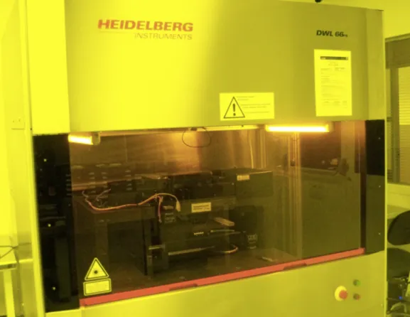
Next step was the patterned exposure of the photoresist for the lift-off process. The lithography pattern is defined by a photomask which has the target pattern written on its Cr-coating. L-Edit software was used for the photomask CAD design. Photomask blanks were delivered as photoresist/chrome/glass from the mask manufacturer (Telic Inc.). These mask blanks were selectively exposed using Heidelberg Instruments DWL-66 Laser Mask Writer with a 4 mm write head (Figure 3.4). Masks became ready to use in lithography process after photoresist development, Cr etching in Cr-etchant solution and photoresist removal and mask cleaning process.
43
Figure 3.4: Heidelberg Instruments DWL-66 laser mask writer used for photomask production.
For the exposure step, Electronic Vision Group EVG 620 mask aligner was used (Figure 3.5). It has a Hg lamp equipped with i-line filter, which produces a collimated UV light-beam with a output wavelength of 365 nm. Exposure was performed with a dose of 40 mJ using soft contact mode. Photoactive compound in the photoresist (DNQ-sulfonate) is converted into indene carboxylic acid upon exposure by exchanging N2 with H2O and attaining several orders of
![Figure 2.7: Ion positions in a quartz lattice with and without external stress [12].](https://thumb-eu.123doks.com/thumbv2/9libnet/5745642.115805/27.892.318.643.188.500/figure-ion-positions-quartz-lattice-external-stress.webp)
![Figure 2.12: Crystal structure and surface free energies for three different planes of ZnO [11]](https://thumb-eu.123doks.com/thumbv2/9libnet/5745642.115805/39.892.334.622.184.527/figure-crystal-structure-surface-free-energies-different-planes.webp)