Letter Vol. 45, No. 24 / 15 December 2020 / Optics Letters 6719
Lithography-free disordered
metal–insulator–metal nanoantennas for
colorimetric sensing
Zeinab Eftekhari,
1,2Amir Ghobadi,
1,3AND
Ekmel Ozbay
1,2,3,*
1NANOTAM-Nanotechnology Research Center, Bilkent University, 06800 Ankara, Turkey2Physics Department, Bilkent University, 06800 Ankara, Turkey
3Department of Electrical and Electronics Engineering, Bilkent University, 06800 Ankara, Turkey
*Corresponding author: [email protected]
Received 15 September 2020; revised 7 November 2020; accepted 10 November 2020; posted 11 November 2020 (Doc. ID 410213); published 10 December 2020
The colorimetric detection of bio-agent targets has attracted considerable attention in nanosensor designs. This plat-form provides an easy to use, real-time, and rapid sensing approach, as the color change can be easily distinguished by the naked eye. In this Letter, we propose a large scale compatible fabrication route to realize colorimetric optical nanosensors with a novel configuration. For this pur-pose, we design and fabricate a tightly packed disordered arrangement of Fabry–Perot based metal–insulator–metal nanoantennas with a resonance frequency at visible light wavelengths. In this design, the adsorbed bio-agent changes the effective refractive index of the cavity, and this causes a shift in the resonance wavelength. The experimental data show that the proposed design can have sensitivity values >70 nm/refractive index unit. Unlike other optical sensing schemes that rely mainly on hot spot formation and field enhancement, this design has a large active area with rela-tively uniform patterns that make it a promising approach for low-level and reliable bio-detection. © 2020 Optical Society of America
https://doi.org/10.1364/OL.410213
Biosensors have revealed their tremendous potential in many applications, including medical diagnosis, food safety, and environmental monitoring. However, their main use is in the detection of analytes and bio-agents such as disease biomarkers and contaminants. Based on the detected signal, biosensors can be classified as optical (such as plasmonic biosensors), electro-chemical, piezoelectric, or magnetic biosensors [1,2]. Among all biosensors, optical biosensors are one of the most commonly used tools for analytical biosensing due to their high sensitivity, specificity, potential for real-time sensing, and cost effectiveness [3,4].
One the most commonly used colorimetric optical sens-ing schemes is based on localized surface plasmon resonances (LSPRs) and propagating surface polaritons (PSPs), since noble metal nanostructures show LSPR in the visible frequencies [5–11]. In this configuration, upon the excitation of LSPRs, absorption and scattering cross sections of noble metallic
nanoparticles are greatly enhanced, and extremely intense and localized electromagnetic fields are created in “hot spots” [12–15]. These high intensity spots enable the devices to track any small change in the dielectric environment surrounding these nanostructures [9]. However, this can also be considered as a drawback for these systems. The non-uniform lateral field intensity in these designs causes a limitation on their detec-tion capability [12,14]. For example, in a periodic design, we have high field localization in the gap between units and low enhancement at the top of the units. Therefore, depending on the location of a bio-agent with respect to the unit, the field enhancement and resonance shift can change. Although a single plasmonic antenna can also be used for detection, the proba-bility of overlapping of a molecule with this single element is quite low. That is why they are not a viable solution for practical use. Besides this technical limitation, these plasmonic sensors are mainly high-cost precious-metal based designs or their fabrication demands expensive tools such as electron beam lithography (EBL), which is not a large scale compatible tool. It should be noted that some innovative EBL-free designs have been proposed in recent years [16,17]. Moreover, dielectric based metasurfaces were found to be promising to replace the precious-metal based plasmonic sensors [18–21].
The above-mentioned scalability requirement can be solved by planar design since they do not need any lithography or patterning. Strong optical interference in metal–insulator (MI) and metal–semiconductor (MS) pair based designs can be used to achieve ultra-broadband perfect absorbers and narrowband color filters [22,23]. The most widely used cavity design color filter is a MI–metal (MIM) configuration. In a typical MIM design, a specific wavelength is absorbed by the cavity and the rest of the spectrum gets reflected. This creates a set of subtrac-tive colors called the CMY (cyan-magenta-yellow) model. In a recent paper, we showed that high efficiency RGB (red-green-blue) colors can be made using Bi metamaterials [24]. However, the resonance frequency of an MIM color filter is defined by the spacer layer thickness and refractive index, which has no contact with the surrounding environment. That is why these
6720 Vol. 45, No. 24 / 15 December 2020 /Optics Letters Letter
planar cavity designs have been rarely used for sensing applica-tions [25–27]. To be able to use them in sensing applicaapplica-tions, nanostructuring is needed to provide an area for interaction with the surrounding environment. However, in the meantime, the fabrication route for nanostructuring should be large scale compatible.
In this Letter, we develop a lithography-free nanostructured MIM design for colorimetric sensing application. In other words, the proposed design is a Fabry–Perot (FP) based dis-ordered arrangement of densely packed MIM nanoantennas. In this design, the target analyte can diffuse inside the gaps and tune the spacer effective refractive index and this, in turn, causes a peak resonance shift and color change. To design and analyze this system, we first perform finite-difference-time-domain (FDTD) simulations on a planar configuration. Later, to estimate the effect of the induced randomness, a transfer matrix method (TMM) theoretical analysis is conducted. Finally, the optimized design is fabricated and characterized. To obtain a nanostructured spacer layer, the oblique angle deposition technique is used, which is a room temperature and large scale compatible approach with no material limitation. Based on the obtained optical results, visible light colors can be realized with this MIM antenna design. Upon deposition of a dielectric layer (as the modeling agent for biomarkers), the resonance frequency is red-shifted, and a sensitivity as high as ∼84 nm/refractive index unit (RIU) can be achieved. Moreover, the color (position of resonance peak) of the MIM biosensor can be passively adopted by the spacer layer thick-ness. The proposed design strategy offers a highly sensitive, robust, and compact biomolecular diagnostics with a real-time, label-free, and early point-of-care diagnosis that can be used in various applications such as drug detection and environmental monitoring.
To gain insight on the resonance condition of a Bi based MIM design, we initially begin our analysis using a planar design model, as shown in Fig.1(a). The spacer layer is made of lithium fluoride (LiF) with a thickness ofDI. The bottom and top layers are Bi. The top layer thickness isDM, while the bottom layer is an optically thick layer with no transmission in the visible range. To realize the influence of the geometrical dimensions upon the absorption response, we utilized the Lumerical (FDTD) simula-tion package. In the FDTD simulasimula-tions, we illuminated the unit cell with a broadband plane wave at normal incidence whose electric field is polarized in thex direction. Prior to these
sim-ulations, the permittivity values of bulk Bi and LiF layers were experimentally extracted using a spectroscopic ellipsometer, as explained in detail in our previous work [24]. The permittivity data of Bi are shown in Fig.1(b). Due to superior matching of the Bi permittivity data with that of an ideal absorber, the MIM design can absorb all of the frequencies except for the ones with constructive interference. This can be seen from the absorp-tion contour plot shown in Fig.1(c). As this panel implies, the incident light is dominantly absorbed in the top layer, and it shows a notch in the middle of the simulated spectrum. With this design, a spectrally selective reflection peak can be achieved, and a reflective RGB color filter can be realized. To optimize the color purity, we need to reduce the full-width-at-half-maximum (FWHM) of the reflection peak and broaden the absorption bands to avoid multi-color reflection. For this purpose, the top layer thickness is initially swept while the spacer layer thickness is fixed at 150 nm. Figure1(d) shows the dependence of the reflection spectra of the MIM design to DM. As implied from
Fig. 1. (a) Schematic representation of the proposed MIM cavity with its (b) extracted spectral permittivity of Bi (both real and imagi-nary) in our desired range of 300–1000 nm. (c) Two-dimensional profile of the absorbed power across the MIM cavity as a function of incident light wavelength. Sweep and optimization of reflection spectra for different geometries of (d)DM(whileDIis fixed at 150 nm) and
(e)DI(whileDMis fixed at 20 nm).
this plot, as DM increases, the FWHM of reflection gradually narrows. However, at large dimensions, a new reflection peak starts to appear in off-resonance frequencies. Therefore, a trade-off should be followed to have the best color purity, and for this,DMis depicted as 20 nm. In the next step, the spacer layer influence on the reflection response of the MIM cavity is inves-tigated, as shown in Fig.1(e). In this panel, the reflection peak experiences a nearly linear red shift as the thickness increases. Therefore, based on the desired color, theDIcan be modified to tune the spectral position of the reflection peak.
All of the above-mentioned results prove the RGB color generation of a planar Bi based MIM cavity. Yet, the spectral position of this MIM cavity is defined by the spacer optical thickness (both thickness and refractive index). Therefore, a change in color requires a tuning on the spacer layer. However, in a planar configuration, this layer is capped by the top metal absorber, and it has no interaction with an outside dielectric region that is air. Due to this reason, it cannot be a good option for the colorimetric optical sensing of an unknown agent. To make it functional for sensing purposes, nanostructuring should be introduced into this architecture to enhance its active surface area. In other words, the planar MIM layer should be split into sub-wavelength MIM nanoantennas with ultra-small gaps for sensing agent diffusion.
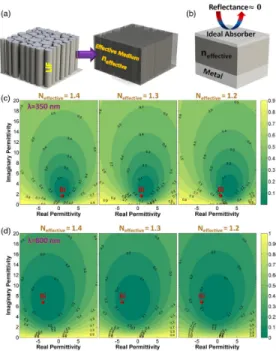
Therefore, instead of a bulk LiF layer, we need to have nanorod (NR) designs. However, the question is, “Can we keep the reflective color generation property of planar MIM design in a nanoantenna MIM configuration?” Based on effective medium theory, sub-wavelength dielectric geometries can be modeled as a bulk system with an effective refractive index that is a value between air and dielectric indices, as shown in Fig.1(a). To predict the absorption response of this effective medium MIM design, we use a modeling approach based on TMM. As explained in detail in our previous studies [22,24] in this model, we fix the geometries (DI=150 nm andDM=20 nm) and the spacer layer material (as LiF) and look for an ideal absorber material data (with near zero reflection) for the top
Letter Vol. 45, No. 24 / 15 December 2020 /Optics Letters 6721
coating. Then, we compare this ideal material permittiv-ity data with that of Bi. Figure 1(b) shows our model used in TMM modeling. For this design, the reflection contour plots have been extracted as a function of top material real [Re(ε)] and imaginary [Im(ε)] permittivity parts. In these panels, for instance, staying within a 0.1 circle means that the MIM design is below 10% reflection at that wavelength. These contour plots have been acquired for three different spacer effective refractive indices (Neffective) of 1.4, 1.3, and
1.2 to simulate different LiF NR filling fractions. The reso-nance wavelengths of 350 and 800 nm are chosen for these plots, since the light absorption of the Bi top layer is maximum at these wavelengths. For 350 nm incident light wavelength [Fig. 2(c)], reducing the Neffective causes a slight shift in the
reflection circles. However, in all three conditions, Bi data stay within a 0.2 circle. The same holds for the 800 nm excitation, as exhibited in Fig. 2(d). Therefore, nanostructuring of LiF does not ruin the absorption optical response of the MIM cavity. Specifically, in the case of high Neffective, we can have a
quite similar response with the planar design. This implies that higher packing density is more favorable. On the other hand, in all panels, the ideal point (zero reflection point) shifts toward more negative Re(ε), as the effective refractive index increases. Looking at the Bi permittivity data, we can see that as the wavelength increases, the Re(ε) moves toward negative values. This matching is quite promising from sensing the point of value. This means that as we expose these MIM nanoantennas to a biomarker adsorption, theNeffectiveincreases and the reflection
dip shifts toward longer wavelengths. All of these theoretical calculations predict the high functionality of a tightly packed MIM nanoantenna absorber in colorimetric sensing.
In the next step, we have to find a fabrication route to realize these LiF NRs in large scales. Among the various large scale com-patible nanostructuring techniques, oblique angle deposition is
Fig. 2. (a) Schematic illustration of the real LiF NR design and its effective medium model. (b) MIM ideal absorber used to extract the reflection contour plots. TMM extracted reflection contour plots for three differentNeffectiveof 1.4, 1.3, and 1.2 for incident light wavelengths of (c) 350 nm and (d) 800 nm.
an effective approach to fabricate nanostructures with no mate-rial restriction.
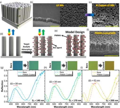
Specifically, for dense high aspect ratio structures, where the EBL becomes challenging, this approach can provide a robust solution. Figure3(a) schematically depicts the proposed MIM nanoantenna design with multiple NR radii. Every NR is capped with a thin Bi layer. To realize this design configuration, we first deposit a 150 nm Bi layer on a diced Si substrate. This layer is coated by the thermal evaporation technique (VAKSIS tool). The deposition rate is set at ∼2 Å/s, and the chamber pres-sure is kept below 5E-6 Torr throughout the process. Afterward, oblique angle deposition is utilized to fabricate LiF NRs, as explained in detail in our previous study [24]. The deposition conditions are the same as the Bi layer, except that the rate is 5–6 Å/s to create a better nanotexturing. Finally, a 20 nm thick Bi layer is coated on top of the NRs to complete the fabrication of disordered MIM nanoantennas. It should be noted that the size of the samples are 1 cm × 1 cm. Due to the large scale compatibility of the fabrication route, this dimension can be up scaled. To verify the formation of this hybrid design, scanning electron microscopy (SEM) imaging is utilized. Figure 3(b) exhibits the existence of standing tightly packed LiF NRs with sub-wavelength radii. According to Fig.3(c), the deposition of a Bi thin film has not led to continuous layer formation, and the surface morphology has not changed. Therefore, a biomarker analyte can diffuse within its small gaps and tune the cavity’s effective index. In this way, upon adsorbent deposition, the res-onance wavelength shifts and consequently the color changes. This is graphically explained in Fig.3(d). To demonstrate the biosensing capability of our disordered MIM nanoantenna, a model design is used, as shown in Fig.3(e). To model these bio-agent analytes, we spin-coated the MIM cavity with 495Poly (methyl methacrylate) (495PMMA) A2 to coat the NR sur-faces and the gaps in between, as depicted in the SEM image in Fig.3(f ).
To evaluate the colorimetric response of this disordered MIM nanoantenna array design, the optical reflection response of the structure is evaluated for three differentDIvalues of 140, 170, and 200 nm [Figs.3(g)–3(i)]. The three different thicknesses are used to generate three different colors. The reflection spectra of these MIM nanoantennas, in the range of 350–950 nm, before and after PMMA coating are measured using a home-made setup. In this setup, a halogen lamp is used as the light source, integrated with a microscope to collect the reflection data. These collected reflection data are transferred into a spec-trometer (Newport Corporation; Irvine, CA, USA) (Newport OSM2). In all of the measurements, the obtained reflection values are normalized with that of a thick Al sheet. To have a better visualization, the optical image of the samples before and after coating are shown on top of the spectral reflection plot. For the case ofDI=140 nm, the PMMA coating has caused a 39 nm shift in the reflection peak position. Taking the PMMA refractive index to be ∼1.5 in these frequencies, the maxi-mum experimental sensitivity of the nanosensor is recorded as Smax=1λ/1n = 39 nm/(1.5−1.0) = 72 nm/RIU. The
same characterization is also conducted onDI=170 nm, and 200 nm, where the resonance red shift is found to be 34 and 42 nm (corresponding to theSmaxvalues of 68 and 84 nm/RIU).
Overall, this work demonstrates a design strategy to realize a sensitive, real-time, and label-free optical biosensing scheme. The proposed route is a large scale and extendable approach that can be adopted for other MI combinations. The detailed
6722 Vol. 45, No. 24 / 15 December 2020 /Optics Letters Letter
Fig. 3. (a) Simplified schematic illustration of the disordered MIM nanoantennas design. SEM images of (b) bare LiF NRs and (c) those coated with a thin Bi layer. (d) Operation principle of our proposed biosensor. (e) Model design and (f ) its cross sectional SEM image. In all of the SEM images, the bar length is 400 nm. Reflection spectra of bare and PMMA coated MIM nanoantenna samples for three differentDIvalues of
(g) 140 nm, (h) 170 nm, and (i) 200 nm. At the top of this linear plot, the optical images of bare and PMMA coated samples are depicted.
design, analysis, and characterization results show the unprec-edented potential of this random plasmonic platform for many optoelectronic applications.
Disclosures. The authors declare no conflict of interest. REFERENCES
1. C. I. L. Justino, A. C. Duarte, and T. A. P. Rocha-Santos,Sensors17, 2918 (2017).
2. R. Samson, G. R. Navale, and M. S. Dharne,3 Biotech10, 385 (2020). 3. J. Liu, M. Jalali, S. Mahshid, and S. Wachsmann-Hogiu,Analyst145,
364 (2020).
4. C. Chen and J. Wang,Analyst145, 1605 (2020). 5. J. Homola,Chem. Rev.108, 462 (2008).
6. L. Chen, L. Chan, X. Fu, and W. Lu,ACS Appl. Mater. Interfaces5, 284 (2013).
7. K. Saha, S. S. Agasti, C. Kim, X. Li, and V. M. Rotello,Chem. Rev.112, 2739 (2012).
8. P. D. Howes, S. Rana, and M. M. Stevens,Chem. Soc. Rev.43, 3835 (2014).
9. L. Tang and J. Li,ACS Sens.2, 857 (2017).
10. G. Qiu, Z. Gai, Y. Tao, J. Schmitt, G. A. Kullak-Ublick, and J. Wang,
ACS Nano14, 5268 (2020).
11. X. Han, K. Liu, and C. Sun,Materials (Basel)12, 1411 (2019). 12. J. Jiang, X. Wang, S. Li, F. Ding, N. Li, S. Meng, R. Li, J. Qi, Q. Liu, and
G. L. Liu,Nanophotonics7, 1517 (2018).
13. N. Kongsuwan, X. Xiong, P. Bai, J. Bin You, C. E. Png, L. Wu, and O. Hess,Nano Lett.19, 5853 (2019).
14. D. Radziuk and H. Moehwald,Phys. Chem. Chem. Phys.17, 21072 (2015).
15. H. Wei, S. M. Hossein Abtahi, and P. J. Vikesland,Environ. Sci. Nano
2, 120 (2015).
16. C. Q. Nguyen, W. J. Thrift, A. Bhattacharjee, S. Ranjbar, T. Gallagher, M. Darvishzadeh-Varcheie, R. N. Sanderson, F. Capolino, K. Whiteson, P. Baldi, A. I. Hochbaum, and R. Ragan,ACS Appl. Mater. Interfaces10, 12364 (2018).
17. W. J. Thrift, C. Q. Nguyen, M. Darvishzadeh-Varcheie, S. Zare, N. Sharac, R. N. Sanderson, T. J. Dupper, A. I. Hochbaum, F. Capolino, M. J. Abdolhosseini Qomi, and R. Ragan,ACS Nano11, 11317 (2017).
18. D. U. Yildirim, A. Ghobadi, M. C. Soydan, M. Gokbayrak, A. Toprak, B. Butun, and E. Ozbay,J. Phys. Chem. C123, 19125 (2019).
19. O. Yavas, M. Svedendahl, P. Dobosz, V. Sanz, and R. Quidant,Nano Lett.17, 4421 (2017).
20. N. Bontempi, K. E. Chong, H. W. Orton, I. Staude, D. Y. Choi, I. Alessandri, Y. S. Kivshar, and D. N. Neshev,Nanoscale 9, 4972 (2017).
21. F. Yesilkoy, E. R. Arvelo, Y. Jahani, M. Liu, A. Tittl, V. Cevher, Y. Kivshar, and H. Altug,Nat. Photonics13, 390 (2019).
22. A. Ghobadi, H. Hajian, B. Butun, and E. Ozbay,ACS Photon.5, 4203 (2018).
23. C. Ji, K. T. Lee, T. Xu, J. Zhou, H. J. Park, and L. J. Guo,Adv. Opt. Mater.5, 1700368 (2017).
24. A. Ghobadi, H. Hajian, M. Gokbayrak, B. Butun, and E. Ozbay,
Nanophotonics8, 823 (2019).
25. S. Ayas, G. Bakan, E. Ozgur, K. Celebi, G. Torunoglu, and A. Dana,
Opt. Lett.43, 1379 (2018).
26. M. Serhatlioglu, S. Ayas, N. Biyikli, A. Dana, and M. E. Solmaz,Opt. Lett.41, 1724 (2016).
27. M. Elkabbash, K. V. Sreekanth, Y. Alapan, M. Kim, J. Cole, A. Fraiwan, T. Letsou, Y. Li, C. Guo, R. M. Sankaran, U. A. Gurkan, M. Hinczewski, and G. Strangi,ACS Photon.6, 1889 (2019).