Self-Assembled Molecular Films of Alkanethiols on Graphene for
Heavy Metal Sensing
Nasima Afsharimani,
*
,†Berkin Uluutku,
†Verda Saygin,
†and Mehmet Z. Baykara
*
,†,‡,§ †Department of Mechanical Engineering, Bilkent University, Ankara 06800, Turkey‡UNAM− Institute of Materials Science and Nanotechnology, Bilkent University, Ankara 06800, Turkey §Department of Physics, Harvard University, Cambridge, Massachusetts 02138, United States
ABSTRACT: We report a comparative study involving the
formation of self-assembled molecular films by two types of alkanethiols (1-octadecanethiol and 1-dodecanethiol) on graphene grown via chemical vapor deposition, for heavy metal sensing applications. Scanning tunneling microscopy measurements confirm that the alkanethiol molecules can form localized, ordered molecular films on single-layer graphene despite the presence of structural and chemical irregularities. To test and compare the sensory characteristics associated with graphene functionalized by 1-octadecanethiol and 1-dodecanethiol, graphene-basedfield effect transistors are fabricated via photolithography on silicon dioxide substrates. Devices based on graphene functionalized with
1-octadecanethiol are successfully employed to demonstrate the detection of mercury and lead ions at the 10 ppm level via Dirac point shifts, with a notable difference in response associated with the use of different heavy metal ions. On the other hand, devices based on graphene functionalized with 1-dodecanethiol exhibit p-type character, before and/or after exposure to heavy metal ions, complicating their use in heavy metal sensing in a straightforward fashion via Dirac point shifts.
■
INTRODUCTIONThe exceptional physical and chemical properties of graphene have made it the focus of extensive theoretical and experimental research in the past decade.1−3 Among a large variety of proposed applications, graphene-based chemical and biological sensors are especially promising because graphene’s electronic properties change significantly upon adsorption of particular atomic and molecular species.4−9 Despite this fact, a major limitation associated with the use of graphene in chemical sensing involves the fact that graphene consists of carbon atoms held together by strong covalent bonds, and as such, graphene exhibits weak chemical affinity and specificity toward other atoms and molecules in its vicinity.
A particular strategy to overcome the inherent inertness and low specificity of graphene toward targeted atomic and molecular species involves its chemical modification (i.e., functionalization) with organic and inorganic molecules that either chemisorb or physisorb on graphene, through covalent or noncovalent interactions, respectively.10−13 Functionalized graphene can be then integrated into field-effect transistor (FET) devices in order to detect specific chemicals in the environment. The principle of operation involves the fact that the molecules used to functionalize graphene capture the target species with high specificity, which in turn causes changes in the electrical characteristics of graphene (e.g., the location of the Dirac point), which are subsequently detected as a change in the current−voltage (I−V) characteristics of the FET.
Within this context, the detection of heavy metal ions in aqueous solutions is of particular interest for human health and environmental safety reasons.9,14−17 As the bare graphene surface does not selectively adsorb heavy metal ions, its functionalization by molecules which display particular affinity toward these species is required for such an application. For instance, in a study performed by Sudibya et al., FETs based on reduced graphene oxide functionalized via two types of proteins (calmodulin and metallothionein type II) were fabricated for real-time detection of various metal ions in aqueous solution, including calcium (Ca2+) and mercury (Hg2+).18In this work, pyrene linker molecules have been employed tofirmly attach the proteins to the graphene oxide surface. In another study, the detection of mercury ions (Hg2+) by FET sensors based on
reduced graphene oxide sheets decorated with thioglycolic-acid-functionalized gold nanoparticles has been reported.19 While successful detection of a variety of heavy metal ions has been demonstrated, the hybrid sensor requires the completion of complex fabrication steps such as electrospraying and electro-static force directed assembly. On the other hand, a surface functionalization method relying on weak noncovalent interactions with the graphene surface and a straightforward fabrication procedure is desirable to (i) preserve the unique electrical characteristics of graphene and (ii) retain the Received: September 25, 2017
Revised: November 13, 2017 Published: December 12, 2017
pubs.acs.org/JPCC Cite This:J. Phys. Chem. C 2018, 122, 474−480
Downloaded via BILKENT UNIV on February 25, 2019 at 12:50:20 (UTC).
practicality of the devices for large-scale production. The work by Zhang et al. constitutes an important step toward this direction, where mechanically exfoliated graphene function-alized by a self-assembledfilm of physisorbed 1-octadecanethiol molecules has been employed for Hg2+detection at the 10 ppm level,12based on the previously demonstrated strong affinity of thiol groups toward heavy metal ions.20 However, the use of mechanically exfoliated graphene limits the applicability of the proposed devices in terms of practicality and production volume. Moreover, open questions remain regarding the effects of using different alkanethiol molecules and different heavy metal ions on the detection characteristics of the devices.
Based on the perspective outlined above, we present here a comparative study involving the fabrication of FET devices based on graphene grown by chemical vapor deposition (CVD) and functionalized by two types of alkanethiols (1-octadecane-thiol, ODT, and 1-dodecane(1-octadecane-thiol, DDT) and their use toward the detection of two types of heavy metal ions (mercury, Hg2+
and lead, Pb2+). Motivated by previous studies of alkanethiol adsorption on highly oriented pyrolytic graphite (HOPG) in the literature21−25 and to confirm the formation of molecular films with nanometer-scale spatial resolution, we additionally report the results of scanning tunneling microscopy (STM) measurements performed on functionalized graphene under ambient conditions. The presented data demonstrate the local formation of ordered molecular films by the two alkanethiols on the CVD graphene surface. While graphene functionalized with ODT is successfully implemented in FET devices toward the detection of heavy metal ions in aqueous solutions based on Dirac point shifts, FET devices based on DDT-functionalized graphene are found to exhibit p-type character (before and/or after exposure to heavy metal ions), complicating their implementation toward heavy metal sensing in a straightfor-ward fashion.
■
EXPERIMENTAL DETAILSSingle-layer graphene was grown on copper foils in a quartz tube furnace via the CVD method and then transferred onto highly doped silicon wafer chips covered by 100 nm-thick silicon dioxide (SiO2) according to well-established procedures in the literature.26Subsequently, Raman spectroscopy (WITec alpha300 S) was used to confirm the single-layer character of graphene grown by CVD (Figure 1).27For overall structural characterization, scanning electron microscopy (SEM, FEI Nova NanoSEM 600) was utilized. To establish electrical contact to graphene samples for STM imaging, samples were
covered by several strips of 2 mm-wide and 100 nm-thick gold deposited via thermal evaporation using a shadow-mask-based method.Figure 2shows a picture of the sample prepared for STM imaging as well as an SEM image of a region on the sample featuring graphene situated between two gold electro-des.
ODT and DDT molecules were procured from Alfa Aesar and Sigma-Aldrich, respectively. Ethanol was obtained from Ildam Kimya. All chemicals were used without further purification. ODT powder was dissolved in ethanol to produce solutions of 5 mg mL−1(17 mM) concentration. As DDT is in liquid form, solutions of this molecule were prepared by diluting pure DDT with ethanol to achieve a concentration of 5 mg mL−1(25 mM). For STM measurements, solutions were first drop-cast in volumes of 2.5−5.0 μL onto the surface of CVD-grown graphene situated on SiO2. The STM measure-ments were performed after complete solvent evaporation under ambient conditions with a Nanosurf EasyScan 2 STM instrument. The tips were mechanically cut from 0.25 mm-diameter Pt/Ir wires (Sigma-Aldritch, 70% Pt−30% Ir). The majority of STM images were acquired in the constant-current mode. For certain images, topographical feedback was slowed down to achieve semiconstant-height conditions under which the“error signal” channel (reflecting deviations in current from the set point value) contained structural information about the surface.
To fabricate the FET devices, source and drain electrodes were formed on graphene-covered SiO2 substrates via a standard UV-photolithography process using the AZ5214E photoresist in positive mode, followed by metallization and lift-off steps. Metallization was performed via thermal evaporation Figure 1. Typical Raman spectrum associated with CVD-grown
graphene transferred onto SiO2. The intensity ratio of∼2.50 between
the 2D and G peaks confirm the single-layer character.
Figure 2.(a) Picture of a graphene sample situated on SiO2substrate
and covered by gold electrodes, ready for STM imaging. Electrical contact between the electrodes and the sample holder is established via conductive epoxy. The sample holder is positioned on the cylindrical piezoelectric scanner of the STM. (b) SEM image of a region on the sample surface depicting graphene between two gold electrodes. Certain structural irregularities (such as a tear in graphene below which the SiO2substrate can be seen) are observed.
of 80 nm-thick gold on 3 nm-thick chromium. The devices were isolated from each other using oxygen plasma etching via an inductively coupled plasma (ICP) system (exposure time: 15 s, pressure: 20 mTorr, O2 flow rate: 99 000 sccm, RF coil
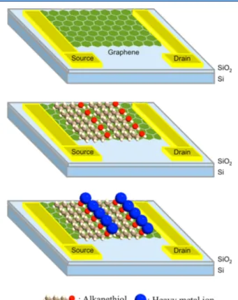
power: 400 000 W, RF platen power: 20 000 W). In the FET devices, the single-layer graphene acts as the electron channel and the highly doped Si substrate works as the gate electrode. For heavy metal sensing experiments, mercury(II) chloride (HgCl2) and lead(II) nitrate (Pb(NO3)2) solutions (Sigma-Aldrich) were diluted in DI water to a concentration of 10 ppm. Minute amounts of heavy metal ion solutions were drop-cast onto alkanethiol-modified graphene-based FETs at room temperature (see Figure 3 for a related schematic). After 20
min, the devices were thoroughly rinsed with DI water and blow-dried with nitrogen. Two-probe electrical characterization of the devices (before and after treatment by heavy metal solutions) was carried out with a semiconductor parameter analyzer (Keithley 4200-SCS). A 5 mV drain voltage was applied in dc mode and the drain current (I) of the devices was monitored as a function of the gate voltage (V) applied through the 100 nm-thick SiO2from beneath the chip. For reference, a
sample I−V measurement on a nonfunctionalized graphene-based FET device is provided inFigure 4.
■
RESULTS AND DISCUSSIONFigure 5shows large-scale STM images of the graphene surface after functionalization by ODT and DDT molecules. When compared with STM images of molecularfilms formed by the same alkanethiols on HOPG,21,23−25 the images obtained on
functionalized graphene exhibit a much more corrugated and structurally irregular character. In particular, corrugated regions are observed which can be attributed to chemical residue from the graphene transfer process (which might be trapped under the graphene or located on top of it),28as well as the inherent corrugation exhibited by graphene due to an interplay between its out-of-plane rigidity and interactions with the substrate.29 Nevertheless, for both ODT- and DDT-functionalized graphene, the existence of localized, ordered regions charac-terized by the imaging of self-assembled molecular“stripes” is observed (see the white arrows in Figure 5a and the white dashed rectangle inFigure 5b). Moreover, the weak character of the noncovalent interactions exhibited by alkanethiol molecules with graphene are confirmed by the frequent occurrence of spontaneous lateral displacement events during imaging (such as the one highlighted by the dashed white rectangle inFigure 5a) due to tip−sample interactions.
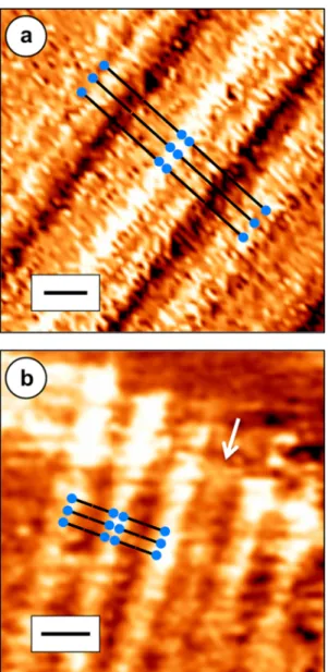
In order to investigate the molecular arrangement associated withfilms formed by ODT and DDT molecules in more detail, short-scale STM measurements have been performed on surface regions exhibiting molecular order (Figure 6). In particular, Figure 6a shows a frequently observed, parallel-striped arrangement for ODT molecules on graphene, similar to the results presented by Zhang et al.12Based on a number of prior studies, it is well established that the thiol end groups in alkanethiols exhibit a significantly higher local density of states (LDOS) when compared with the alkyl chains.30 As STM images reflect contours of constant LDOS,31 we assign the bright positions in high-resolution STM images such asFigure 6a to the thiol end groups associated with the alkanethiols while the darker parts of the images can be attributed to the alkyl chains. In Figure 6a, the bright stripes associated with the molecularfilm formed by ODTs exhibit a periodicity of ∼5.0 nm, about two times the length of a single ODT molecule.21,25 Consequently, we propose that the ODT molecules are arranged in a head-to-head configuration on graphene,12 as shown by the overlaid molecular model. Somewhat similarly,
Figure 6b shows a short-scale STM image of self-assembled DDT molecules on graphene. The molecules are again observed to arrange in parallel stripes where the main periodicity perpendicular to the bright stripes is measured as ∼3.2 nm, about two times the length of a single DDT molecule.24As such, we can again make the proposition that Figure 3. Schematic drawings depicting the graphene-based FET
devices in their bare (top), alkanethiol-functionalized (middle), and finally, heavy-metal-exposed (bottom) states. Please note that a representative alkanethiol (1-hexanethiol) has been employed for visualization purposes.
Figure 4.Transport measurements associated with a FET device based on nonfunctionalized graphene, featuring ambipolar behavior and a Dirac point located at a gate voltage value of about−18 V. The Journal of Physical Chemistry C
DDT mainly self-assembles in a head-to-head configuration on graphene, as shown by the overlaid molecular model. However, irregularities associated with the proposed arrangements are often observed, as for instance signified by the detection of an additional bright stripe indicated by the white arrow inFigure 6b. It also needs to be mentioned that orderedfilms formed by DDT molecules on the graphene surface proved to be considerably smaller in number when compared with those formed by ODT molecules and their stable imaging also required the application of a more closely controlled set of parameters. These observations could be potentially attributed to the smaller chain length of DDT molecules when compared with ODT, which tend to decrease thermodynamic stability,32 an effect that could become evident under the presence of weak noncovalent interactions with the substrate.
While the STM measurements summarized above have established the existence of localized molecularfilms formed by alkanethiols on graphene, it needs to be confirmed whether the localized molecular films formed by ODT and DDT can be employed for the detection of low concentrations of heavy metal ions when integrated into FET devices. The results of related experiments performed with graphene-based and alkanethiol-functionalized FETs are summarized below.
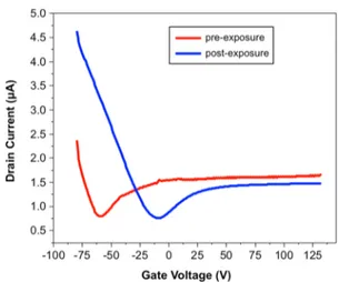
Figure 7shows electrical transport characteristics of an ODT-modified graphene FET measured before and after being treated with an aqueous solution of lead ions. The red curve shows the drain current plotted against the applied gate voltage before the application of the heavy metal solution. On the other hand, the blue curve was measured for the same device after Figure 5.(a) Large-scale STM image (error signal) of the graphene
surface functionalized by ODT molecules. Local formation of molecularfilms is indicated by the white arrows. Tip-induced lateral displacement of ODT molecules on the graphene surface is highlighted by the dashed white rectangle (bias voltage: 600 mV, average tunneling current: 200 pA, scale bar: 50 nm). (b) Large-scale STM image of the graphene surface functionalized by DDT molecules. Local formation of molecularfilms is indicated by the dashed white rectangle (bias voltage: 600 mV, tunneling current: 300 pA, scale bar: 20 nm).
Figure 6.(a) Short-scale STM image (error signal) of the graphene surface functionalized by ODT molecules. The proposed molecular arrangement (head-to-head) is overlaid on the image, with thiol end groups highlighted by blue circles (bias voltage: 600 mV, average tunneling current: 200 pA, scale bar: 2 nm). (b) Short-scale STM image of the graphene surface functionalized by DDT molecules. The proposed molecular arrangement (head-to-head) is overlaid on the image, with thiol end groups highlighted by blue circles. An additional bright stripe (not in agreement with the head-to-head arrangement) is highlighted by the white arrow (bias voltage: 600 mV, tunneling current: 200 pA, scale bar: 3 nm).
exposure to the 10 ppm heavy metal solution, as explained in theExperimental Detailssection. It can be clearly observed that the Dirac point of the graphene-based FET device shifted about 50 V upon heavy metal exposure. The shift is toward positive voltages, consistent with previous studies of heavy metal adsorption on functionalized graphene.12,18The measurements were repeated with several individual devices, with both lead and mercury solutions, and average Dirac point shifts of 30.2± 6.8 and 7.1 ± 4.8 V were obtained, for lead and mercury, respectively. Thus, the capability of our ODT-functionalized graphene-based FET devices to function as heavy metal sensors is confirmed. Additionally, the consistently higher values of Dirac point shifts measured for lead exposure potentially point to a stronger affinity exhibited by thiols toward lead ions, when compared with mercury ions.33 Finally, the remarkable similarity in Dirac point shift values measured with our ODT-functionalized devices based on CVD graphene upon mercury adsorption (7.1± 4.8 V) and those devices reported in the literature based on mechanically exfoliated graphene (6.2± 2.0 V)12needs to be emphasized.
Electrical transport measurements associated with a single DDT-modified graphene FET, before and after treatment by mercury solution, are presented inFigure 8. While the device initially features a well-defined Dirac point around 20 V, exposure to the heavy metal solution causes a strong shift in the transport characteristics toward p-type behavior, such that the minimum conductivity point extends beyond the maximum value of the applied gate voltage (+80 V). As such, it is not possible to characterize the response of the FET to heavy metal exposure as a well-defined shift in the Dirac point. Additionally, it needs to be mentioned that for certain FET devices based on graphene functionalized with DDT, p-type behavior is observed even before heavy metal adsorption (see, e.g., the I−V curves presented inFigure 9). While one could argue that a change in drain current values at a given gate voltage upon heavy metal adsorption could be used for sensing purposes for such devices,8 the downward shift in current values upon heavy metal adsorption exhibited by the device in Figure 9, when contrasted with the opposite trend shown by the device in
Figure 8, further underlines the inconsistent and, as such, unfavorable characteristics of DDT-functionalized devices for heavy metal detection. It should be indicated that the
observation of p-type behavior for all investigated devices (before and/or after heavy metal exposure) rules out fabrication-specific effects (such as the chemical cleanliness of the specific graphene sample used for a given device) as potential reasons behind the unfavorable characteristics of the sensors.
Physical and chemical mechanisms responsible for sensing behavior in devices based on carbon-based nanomaterials (such as carbon nanotubes and graphene) are still under debate. The work of Heller et al. has identified potential mechanisms, including electrostatic gating and capacitance effects, as well as associated signatures in I−V curves.34The electrostatic gating effect manifests as a noticeable shift of the I−V curve along the gate voltage (i.e., horizontal) axis, induced by a modification of the strength of the field effect acting on the carbon-based material upon adsorption of target species, which leads to p- or n-type doping and a corresponding change in the position of the Dirac point. On the other hand, the capacitance effect Figure 7.Transport measurements associated with a FET device based
on ODT-functionalized graphene, before and after exposure to a 10-ppm lead solution. The positive shift in the position of the Dirac point is clearly detected.
Figure 8.Transport measurements associated with a FET device based on DDT-functionalized graphene, before and after exposure to a 10-ppm mercury solution. While the device exhibits a well-defined Dirac point around 20 V before exposure (in conjunction with ambipolar transport characteristics), postexposure measurements reveal p-type behavior until the maximum gate voltage of 80 V.
Figure 9.Transport measurements associated with a FET device based on DDT-functionalized graphene, before and after exposure to a 10-ppm lead solution. The device exhibits p-type behavior until the maximum gate voltage of 80 V, both before and after heavy metal exposure. A downward shift in the drain current upon heavy metal adsorption is observed.
causes a noticeable broadening in the I−V curves, and consequently the reduced capability to control the drain current via the application of the gate voltage, which is induced by the low electrical permittivity of adsorbed species. Among the proposed mechanisms, the electrostatic gating effect is seen to be the predominant effect responsible for the sensing behavior in the majority of our experiments (see, e.g.,Figures 7
and8), as signified by a shift in the position of the Dirac point toward more positive values. As suggested before,18 the underlying mechanism could involve a conformational change in the alkanethiol molecules upon heavy metal adsorption, resulting in a closer separation between the electron-rich thiol groups of the molecules and the graphene surface, thus strengthening the associatedfield effect leading to p-doping in graphene. The consistent observation of positive Dirac point shifts in the sensing experiments supports this hypothesis. On the other hand, a broadening of I−V curves associated with the proposed capacitance effect is not observed in the great majority of the measurements, which is to be expected as such an effect would require the almost-complete coverage of the graphene surface by alkanethiol molecules,34 which is not
realized in our devices as confirmed by STM imaging
experiments. Within this context, one could speculate that the different behavior exhibited by devices based on ODT- and DDT-functionalized graphene arises from the different size of the molecules. In particular, the shorter chain length of DDT molecules could (in the presence of similar packing arrange-ments, as demonstrated inFigure 6) lead to a higher density of thiol groups forming on the graphene surface, which would result in a stronger response to heavy metal adsorption such that Dirac points could now extend beyond the maximum applicable gate voltage values (Figure 8). Moreover, devices where the coverage of graphene by DDT is particularly extensive could feature a high degree of p-doping such that the Dirac point is already located beyond the applicable gate voltage range (Figure 9). Nevertheless, a thorough evaluation of the proposed mechanisms requires further experiments.
Finally, since the sensing experiments presented here involve the detection of a single type of heavy metal ion for each measurement, future work could focus on the evaluation of device selectivity toward particular species by performing measurements in aqueous solutions involving two or more types of metal ions. Moreover, while the heavy metal concentration of 10 ppm is low enough to confirm the high sensitivity of the functionalized devices and allow direct comparison to existing results,12 aqueous solutions with a wider range of heavy metal concentrations can be probed in future work for a more complete characterization of device capabilities.
■
CONCLUSIONSWe have demonstrated, via STM measurements performed under ambient conditions, the formation of localized films on CVD graphene by ODT and DDT molecules. Graphene functionalized by ODT and DDT molecules has been implemented into FET devices, which were tested as heavy metal sensors. Devices based on ODT-functionalized graphene successfully detected the presence of mercury and lead ions in aqueous solutions at the 10 ppm level, as a noticeable shift in the position of the respective Dirac points. The stronger response of the sensors to lead ions, when compared with mercury, has been attributed to a stronger affinity exhibited by the thiol groups of molecularfilms toward lead. Devices based
on DDT-functionalized graphene exhibited p-type character (before and/or after heavy metal exposure), such that a straightforward evaluation of sensing performance based on Dirac point shifts was not possible. Nevertheless, our results underline the feasibility of noncovalent functionalization of CVD graphene for chemical sensing applications, which may be extended to target species other than heavy metals with the use of different functionalization agents.
■
AUTHOR INFORMATION Corresponding Authors *E-mail:[email protected]. *E-mail:[email protected]. ORCID Mehmet Z. Baykara:0000-0002-0278-6022 Author ContributionsThe manuscript was written by N.A. and M.Z.B. N.A., B.U., and V.S. performed the STM experiments. N.A. performed the heavy metal sensing experiments. All authors have given approval to thefinal version of the manuscript.
Notes
The authors declare no competingfinancial interest.
■
ACKNOWLEDGMENTSThis work has been financially supported by TUBITAK
through Grant No. 214M129. The authors would like to thank Dr. Evgeniya Kovalska for providing several graphene samples grown on copper foils, Arsalan Nikdoost for practical help regarding photolithography, Dr. Nuri Oncel for helpful discussions, and Dr. Hadi Zareie for generous help with STM experiments.
■
REFERENCES(1) Geim, A. K.; Novoselov, K. S. The rise of graphene. Nat. Mater. 2007, 6, 183−191.
(2) Geim, A. K. Graphene: status and prospects. Science 2009, 324, 1530−1534.
(3) Novoselov, K. S.; Fal’ko, V. I.; Colombo, L.; Gellert, P. R.; Schwab, M. G.; Kim, K. A roadmap for graphene. Nature 2012, 490, 192−200.
(4) Schedin, F.; Geim, A. K.; Morozov, S. V.; Hill, E. W.; Blake, P.; Katsnelson, M. I.; Novoselov, K. S. Detection of individual gas molecules adsorbed on graphene. Nat. Mater. 2007, 6, 652−655.
(5) Fowler, J. D.; Allen, M. J.; Tung, V. C.; Yang, Y.; Kaner, R. B.; Weiller, B. H. Practical chemical sensors from chemically derived graphene. ACS Nano 2009, 3, 301−306.
(6) Cheng, Z. G.; Li, Q.; Li, Z. J.; Zhou, Q. Y.; Fang, Y. Suspended graphene sensors with improved signal and reduced noise. Nano Lett. 2010, 10, 1864−1868.
(7) Kuila, T.; Bose, S.; Khanra, P.; Mishra, A. K.; Kim, N. H.; Lee, J. H. Recent advances in graphene-based biosensors. Biosens. Bioelectron. 2011, 26, 4637−4648.
(8) Mao, S.; Yu, K. H.; Chang, J. B.; Steeber, D. A.; Ocola, L. E.; Chen, J. H. direct growth of vertically-oriented graphene for field-effect transistor biosensor. Sci. Rep. 2013, 3, 1696.
(9) Chang, J. B.; Zhou, G. H.; Christensen, E. R.; Heideman, R.; Chen, J. H. Graphene-based sensors for detection of heavy metals in water: A review. Anal. Bioanal. Chem. 2014, 406, 3957−3975.
(10) Georgakilas, V.; Otyepka, M.; Bourlinos, A. B.; Chandra, V.; Kim, N.; Kemp, K. C.; Hobza, P.; Zboril, R.; Kim, K. S. Functionalization of graphene: Covalent and non-covalent approaches, derivatives and applications. Chem. Rev. 2012, 112, 6156−6214.
(11) Wang, Q. H.; Hersam, M. C. Room-temperature molecular-resolution characterization of self-assembled organic monolayers on epitaxial graphene. Nat. Chem. 2009, 1, 206−211.
(12) Zhang, T.; Cheng, Z. G.; Wang, Y. B.; Li, Z. J.; Wang, C. X.; Li, Y. B.; Fang, Y. Self-assembled 1-octadecanethiol monolayers on graphene for mercury detection. Nano Lett. 2010, 10, 4738−4741.
(13) Englert, J. M.; Dotzer, C.; Yang, G. A.; Schmid, M.; Papp, C.; Gottfried, J. M.; Steinruck, H. P.; Spiecker, E.; Hauke, F.; Hirsch, A. Covalent bulk functionalization of graphene. Nat. Chem. 2011, 3, 279− 286.
(14) Gumpu, M. B.; Sethuraman, S.; Krishnan, U. M.; Rayappan, J. B. B. A review on detection of heavy metal ions in water - An electrochemical approach. Sens. Actuators, B 2015, 213, 515−533.
(15) Aragay, G.; Pons, J.; Merkoci, A. Recent trends in macro-, micro-, and nanomaterial-based tools and strategies for heavy-metal detection. Chem. Rev. 2011, 111, 3433−3458.
(16) Li, M.; Gou, H. L.; Al-Ogaidi, I.; Wu, N. Q. Nanostructured sensors for detection of heavy metals: a review. ACS Sustainable Chem. Eng. 2013, 1, 713−723.
(17) Singh, V.; Mondal, P. C.; Singh, A. K.; Zharnikov, M. Molecular sensors confined on SiOx substrates. Coord. Chem. Rev. 2017, 330, 144−163.
(18) Sudibya, H. G.; He, Q. Y.; Zhang, H.; Chen, P. Electrical detection of metal ions using field-effect transistors based on micropatterned reduced graphene oxide films. ACS Nano 2011, 5, 1990−1994.
(19) Chen, K. H.; Lu, G. H.; Chang, J. B.; Mao, S.; Yu, K. H.; Cui, S. M.; Chen, J. H. Hg(II) ion detection using thermally reduced graphene oxide decorated with functionalized gold nanoparticles. Anal. Chem. 2012, 84, 4057−4062.
(20) Feng, X.; Fryxell, G. E.; Wang, L. Q.; Kim, A. Y.; Liu, J.; Kemner, K. M. Functionalized monolayers on ordered mesoporous supports. Science 1997, 276, 923−926.
(21) Gunning, A. P.; Kirby, A. R.; Mallard, X.; Morris, V. J. Scanning-tunneling-microscopy of various alkanols and an alkanethiol adsorbed onto graphite. J. Chem. Soc., Faraday Trans. 1994, 90, 2551−2554.
(22) Cyr, D. M.; Venkataraman, B.; Flynn, G. W.; Black, A.; Whitesides, G. M. Functional group identification in scanning tunneling microscopy of molecular adsorbates. J. Phys. Chem. 1996, 100, 13747−13759.
(23) Sheng, H. Y.; Fujita, D.; Ohgi, T.; Dong, Z. C.; Jiang, Q. D.; Nejoh, H. Two-dimensional ordering of octadecanethiol molecules on graphite observed by scanning tunneling microscope. Appl. Surf. Sci. 1997, 121-122, 129−132.
(24) Sheng, H. Y.; Dong, Z. C.; Fujita, D.; Ohgi, T.; Nejoh, H. Observation of 1-dodecanethiol molecules on graphite by scanning tunneling microscopy. Ultramicroscopy 1998, 73, 195−198.
(25) Xu, Q. M.; Wan, L. J.; Yin, S. X.; Wang, C.; Bai, C. L. Effect of chemically modified tips on STM imaging of 1-octadecanethiol molecule. J. Phys. Chem. B 2001, 105, 10465−10467.
(26) Li, X. S.; Cai, W. W.; An, J. H.; Kim, S.; Nah, J.; Yang, D. X.; Piner, R.; Velamakanni, A.; Jung, I.; Tutuc, E.; et al. Large-area synthesis of high-quality and uniform graphene films on copper foils. Science 2009, 324, 1312−1314.
(27) Ferrari, A. C.; Meyer, J. C.; Scardaci, V.; Casiraghi, C.; Lazzeri, M.; Mauri, F.; Piscanec, S.; Jiang, D.; Novoselov, K. S.; Roth, S.; et al. Raman spectrum of graphene and graphene layers. Phys. Rev. Lett. 2006, 97, 187401.
(28) Demirbas, T.; Baykara, M. Z. Nanoscale tribology of graphene grown by chemical vapor deposition and transferred onto silicon oxide substrates. J. Mater. Res. 2016, 31, 1914−1923.
(29) Geringer, V.; Liebmann, M.; Echtermeyer, T.; Runte, S.; Schmidt, M.; Ruckamp, R.; Lemme, M. C.; Morgenstern, M. Intrinsic and extrinsic corrugation of monolayer graphene deposited on SiO2.
Phys. Rev. Lett. 2009, 102, 076102.
(30) Giancarlo, L. C.; Flynn, G. W. Raising flags: Applications of chemical marker groups to study self-assembly, chirality, and orientation of interfacial films by scanning tunneling microscopy. Acc. Chem. Res. 2000, 33, 491−501.
(31) Chen, C. J. Introduction to Scanning Tunneling Microscopy, 2nd ed.; Oxford University Press: Oxford, U.K., 2007.
(32) Love, J. C.; Estroff, L. A.; Kriebel, J. K.; Nuzzo, R. G.; Whitesides, G. M. Self-assembled monolayers of thiolates on metals as a form of nanotechnology. Chem. Rev. 2005, 105, 1103−1169.
(33) Yantasee, W.; Warner, C. L.; Sangvanich, T.; Addleman, R. S.; Carter, T. G.; Wiacek, R. J.; Fryxell, G. E.; Timchalk, C.; Warner, M. G. Removal of heavy metals from aqueous systems with thiol functionalized superparamagnetic nanoparticles. Environ. Sci. Technol. 2007, 41, 5114−5119.
(34) Heller, I.; Janssens, A. M.; Mannik, J.; Minot, E. D.; Lemay, S. G.; Dekker, C. Identifying the mechanism of biosensing with carbon nanotube transistors. Nano Lett. 2008, 8, 591−595.