~ Pergamon
Sohd State Commumcauons, Vol. 90, No 2, pp. 77-81, 1994 Elsevier Science Ltd Printed m Great Bntmn. All rights reserved 0038-1098/94 $6.00+.00 0038-1098(94)E0119-VRaman Studies of Doped Polycrystanine Sihcon From Laser-Annealed, Doped a-Si:H A. Compaan, M. E. Savage,
Dept. of Physics and Astronomy, The University of Toledo, Toledo, OH 43606, USA A. Aydinli, and T. Azfar
Dept. of Physics, Bilkent University, Ankara 06533, Turkey (Received 22 December 1993 by M. Cardona)
(Received~otto
20January
1994)We have used Raman scattering to follow the progress of multiple-pulse (sub-melt- threshold) laser annealing in doped hydrogenated amorphous silicon films (a-Si:H) on glass. In phosphorous-doped a-Si:H the Raman signal shows that recrystallization begins with the first laser pulse but that multiple pulses are needed to generate the highest hole concentrations of -,6xl02° cm "3. In boron-doped a-Si:H the electron concentration reaches ~lxl0:1 cm "3 after laser anneal which produces a dip rather than a peak near the phonon line as a consequence of a negative Fano-interference parameter, q. The results show that Raman scattering can be used to obtain carder concentrations in poly-silicon provided that wavelength-dependent Fano interference effects are properly included.
In doped Si, free particle scattering interferes with the discrete phonon Rarnan scattering to produce asymmetric and broadened lineshapes. This Fano lineshape has been studied extensively in heavily-doped crystalline Si 1'2 including pulsed-laser-annealed, ion-implanted layers 3 but has not been examined in the extremely heavily doped poly-Si which can be prepared by pulsed laser recrystallization of hydrogenated amorphous silicon (a- Si:H). 4'5 In this communication we examine the Raman lineshape in heavily doped polycrystalline silicon thin films prepared by pulsed excimer laser annealing of doped a-Si:H thin films grown by plasma-enhanced chemical vapor deposition on glass substrates. 6 In fact the laser-annealed thin films on glass, in spite of their polycrystaUinity, present some advantage for such a study because of the absence of strong scattering from the Si substrate which can obscure some of the features in pulsed-laser-annealed ion- implanted epitaxial layers.
The linewidth and asymmetry of phonon Raman lines has also been used to obtain grain sizes in undoped polycrystalline semiconductors. In this case, the asymmetry arises from the relaxation of wavevector selection rules due to finite wavevector effects in very small crystallites (<100 ,~). This technique was first used in undoped polycrystalline silicon thin films 7 and has subsequently been extended to several other semiconductor systems and also applied to the case of alloy broadening and ion- implantation-produced damage effects. 8 However, doped semiconductors can present problems for such lineshape analyses due to line shape changes and broadening arising from effects of single particle scattering from free carders. Understanding the various contributions to the Raman line shift and shape can improve the utility of Raman scattering as a tool to obtain carder concentrations. This is
77
particularly useful in polycrystalline materials where transport measurements are complicated by grain boundary effects. Transport properties of doped polycrystaUine Si are of considerable interest due the material's use in photovoltaics and thin-film transistors. 9
Previous studies of pulsed-laser-annealed f i l l S of undopexi a-Si:H have shown that a layered structure exists after annealing. Annealing with a picosecond YAG laser ~ and with 10-20 nsec excimer lasers 6 have been shown to form a thin (30 - 100 nm) surface layer which is polycrystallin¢ (grain sizes _> 50 rim). Underneath this lies a microerystalline or free-grained layer (usually observed as a region with grains of 20 m'n diameter or less surrounded by amorphous material 4'1°) of about the same thickness. In addition the laser annealing may produce a layer of a-Si with greatly reduced hydrogen content immediately under the microcrystalline Si. Finally, if the original films are thick enough, there may remain a residual layer of unannealed a-Si:H. We shall use this four-layer model 4 to interpret our Raman dat~
The Raman scattering was performed with two argon laser lines ('k = 457.9 nm and 514.5 nm) and the krypton laser line at ~ = 647.1 nm using a cylindrical focus to avoid beam heating effects. The power density on the sample was below 10 W/era 2. The Raman spectra obtained at Toledo utilized an ISA $3000 triple spectrometer operated in the scanning mode, whereas the data obtained at Bilkent used a JY U1000 double spectrometer. All data were obtained at room temperature with the samples held in air. The Raman probe depths for backscattering [(2a) "1, where ct is the absorption coef-fieient] in crystalline or polycrystalline Si are 0.15 ~tm for ~,--458 nm, 0.30 p,m for 514 nm, and 1.5 ~tm for 647 nm.
78 DOPED POLYCRYSTALLINE SILICON Vol. 90, No. 2
30
25
20 ¸uJ o= 15
Z
10-1
5
1000
,o0
450 460 470 480 490 5605i0
5205~30 54.0
550FREQUENCY
SHIFT (1/cm)
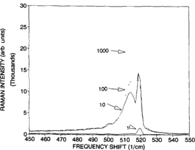
Fig. 1: Raman scattering at ~. = 514.5 nm from phosphorous-doped a-Si:H (n-type) films after 1, 10, 100, and 1000 XeC1 laser pulses at 150 mI/cm 2.
laser annealing with increasing numbers of laser pulses in P-doped a-Si:H is shown in Fil~ure 1. With the pulse energy density of 150 mJ/cm ~, one annealing pulse produces a distinct peak near 520 cm "1 corresponding to the Raman-active (Brillouin-zone-center) mode F25, in crystalline Si. However, with 10, 100, and 1000 pulses, a second peak develops which is shifted downward by -4.5 :i: 0.5 cm". It is also broader and asymmetric.
Although asymmetry may arise from microcrystal- linity due to relaxation of crystal momentum selection rules, 7 this grain size effect is not the cause of the observed broadening in these phosphorous-doped samples. This is confn'med by comparison with similar data obtained on annealed, undoped a-Si:H as shown in Fig. 2a. In this case we have laser annealed a similar, hut undoped a-Si:H film. Similar annealing behavior is observed but in this case the
Raman line does not shift to lower frequencies after additional pulses. (The annealing pulse energy for the undoped film was 300 mJ/cm ~, consistent with the
previously observed higher threshold for multiple-pulse annealing of undoped films.) 5
The shift, broadening, and asymmetry of this second peak in annealed a-Si:H:P films is a result of improved carrier activation with additional pulses. These are characteristic signatures in Raman scattering of n-type electrical activation of the phosphorous dopants. The amount of asymmetry and phonon softening (downward frequency renormalization) increases with dopant concentration.
The effects of n-type doping on the Raman spectra from crystalline Si have been reviewed by Abstreiter and Cardona 11 and the frequency shift in extremely heavily doped crystalline Si has been measured in Raman scattering by Compaan, Contreras, and Cardona 3 For the case of heavily doped n-Si, the continuum of single-particle excitations which interferes with the discrete phonon line arises from inelastic scattering of electrons near the X-point of the conduction band. In general the peak shift and line shape can be used to estimate the doping density. From the shift of 4.5 + 0.5 crn "I observed in Fig. 1 and by comparison with the data of Ref. 3, w e infer that the electron concentration is 6 + 2 x 10²⁰ c m "3.
There are two plausible models for the mixture of doped and undoped material implied by the double peak in the R a m a n scattering. The annealed polycrystalline material m a y have some gFains with few free carriers and others with a high density of free carriers and additional laser pulses simply increase the number of grains or fraction of material with high carrier density. Alternatively the low activation region m a y be confined to a layer below the region of high carrier activation. The spectra of Fig. I do not directly yield an interpretation. However spectra obtained at ~-457.9 run (Fig. 2b) provide the answer. The Raman probe depth at 457.9 nm is only ,.0.15 ttm, whereas
251
a-SI H
i
~
a-SI'H P/ / i/
470 480 4 ~ 500 5;0 520 530 540 FREQUENCY SHIFT (l/cm)b) 457.9 nm
a-Si H t
a-Si H
530
550
FREQUENCY SHIFT (l/cm)Fig. 2: Comparison of Raman scattering from phosphorous-doped a-Si:H film after 1000 laser pulses at 150 mJ/cm 2 and undoped a-Si:H after 1000 pulses at 300 mJ/cm 2. a) Z=514.5 nm; b) Z=457.9 nm.
Vol 90, No. 2 DOPED POLYCRYSTALLINE SILICON 79 at 514.5 nm it is 0.30 14m. Fig. 2b shows that the unshifted
Raman line at 520 cm "1 is absent with 457.9 nm excitation. This indicates that the region of low carrier activation lies beyond the range of the 457.9 nm beam or approximately 0.3 pm below the surface.
Our interpretation is that in the initial stages of laser annealing (fLrst few pulses), recrystallization occurs with the associated evolution of hydrogen from the film. However, the initial crystallites must possess sufficiently high numbers of defects that carrier activation is suppressed. Incomplete H evolution could be a factor leading to suppression of dopant activity. Further annealing with additional pulses removes carrier traps and activates the dopants. The Raman data show that even after 1000 pulses a recrystallized but electrically inactive layer persists deep in the f'flm, presumably near the boundary with the mieroerystalline and/or amorphous material. This boundary layer is simply driven deeper and deeper into the film with increasing numbers of pulses.
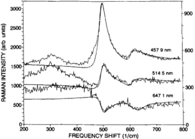
p-type films--Pulsed laser annealing of boron-doped a-Si:H yields extremely heavily doped p-type poly-Si. Figure 3 gives the Raman spectra obtained from these films for three different wavelengths. As observed in p-type crystalline Si, the phonon Raman lineshape near 500 cm q is a strong function of the exciting wavelength. 1 In addition, a second peak is identified just above 600 cm q which is known to arise from the local vibrational modes of lIB and 10B in the Si lattice. 2 The existence of the local mode is clear evidence that the boron is reaching
.Q o') Z LU I-- Z Z < < n.- 3oo Y)O 3OO 0 20O 300 400 500 6O0 700 800 FREQUENCY SHIFT (l/cm)
Fig. 3:
Raman scattering from laser-annealed, boron- doped a-Si:H for three different excitation wavelengths. Baseline is shifted by 1000 for the 457.9 nm data for clarity. The data for 647.1 nm are plotted according to the right hand scale. Dashed curves are fits to the Fano shape as described in the text.substitutional lattice locations, and the interference lineshape is an indication of the electrical activity of the boron. Both results confLrrn that a major fraction of the boron in the poly-Si material is active even though in the amorphous state only a small fraction of the B is electrically active. 12
The asymmetries in the intrinsic phonon mode and in the boron local modes arise from discrete-continuum interactions in which the phonon or local modes interact with the continuum of excitations from inelastic scattering of the holes between valence bands (light-hole, heavy-hole, and spin-orbit split). The Raman lineshapes have been extensively analyzed for doped crys2t~flli~e Si by Cerdeira, et al, 1 and by Chandrasekhar, et al. The solid curve in Figure 3 is a fit of the data to the resulting Fano-type 13 lineshape following Ref. 2:
I(¢0) -- A(qp+r.p)2/(l+ep 2) +
+ B[0.8(qi+ei)2/(l+e, 2) + 0.2(qj+~j)2/(l+ej2)] + C;
with Ep,ij = (CO- C0p,i, j - AO)p,ij)/Fp,ij. Eq. 1 Here the subscripts p, i, and j refer to the intrinsic phonon and the two local modes of lIB and 10B respectively. Clp,, 0.. are the asymmetry parameters which relate to the discrete- continuum mixing, co is the scattering frequency, ¢Op,ij are the original phonon and local mode frequencies, A(Op,ij are the phonon or local mode frequency - - s h i f t s (renormalizations), and Fp,id are the imaginary parts of the phonon or local mode self energies (not including the usual phonon broadening). From Ref. 2 we take the unshifted frequencies as COp = 520 cm "1, ~ = 620 cm "1, and ~ = 644 cm -l. Note that the amplitude factors of 0.8 and 0.2 simply reflect the relative abundances of the two boron isotopes. The parameters used for the fits shown in Fig. 3 are given in Table 1.
For the fits shown in Fig. 3, we have forced the parameters
(Ac~j, qid,
and Fq) of the lIB and 10B local modes to be the same. Thus LXO) i = AC0j, qi ffi qj, and F t = F,. Furthermore we have used the same values of A_COp, A ~ , A~o.., and of F_, F=, F., for all three excitation wavelengths. ByJcomparingVthe 'values of the best fit parameters given in Table I with those of the highest concentration sample of Ref. 1 (4 x 10 z° cm'3), it is easily seen that the free hole concentration is larger than this value and near 1 x 10²¹ em "3 as discussed below.Perhaps the most striking feature of Fig. 3 is the shape of the spectrum obtained with ~. = 647.1 rim. The Raman peak shows up as a dip in the spectrum and the corresponding values of the parameters qp, qi, and qj are negative. The fit to Equation 1 for the 647.1 nm data is not as good as for the shorter wavelengths; and this may Table I: Interference Equation Parameters
~(nrn)
Aa~p qp Fp Ac°id q~l FiJ 457.9 -23+1 4.05:0.5 18-I"1 -16 1.3i-0.5 18 514.5 -23:f.2 2.2._+0.3 18+9- -16 0.7:£-0.3 18 647.1 - 23Y..3 -0.5:£0.2 18+5 -16 -0.3:£0.2 18 A:B:C 1:1.3:3.8 1:1.5:7.7 1:0.5:0.1580 DOPED POLYCRYSTALLINE SILICON Vol. 90, No 2" indicate that the film is not uniformly activated deeper than
about 0.3 grn, as found above for the phosphorous-doped films. This may account for the larger value of F for 647 nm but a more uniform film is unlikely to change the q- parameters substantially. To our knowledge a negative value of the q-parameter in p-type Si has not previously been observed in Raman scattering 1'~ although its physical meaning is readily apparent, as discussed below.
Following the notation of Ref. 2 the qp parameter is given by: 15
qp = (VpTfro +
Aog/r p,
Eq. 2 where Vp is the matrix element of the hole-phonon interaction. Because the phonon scattering matrix element Tp (a third order process) resonates more strongly at the E 1 critical point (3.4 eV) than does the hole scattering matrix element T e (a second order process), the fast term in Eq. 2 dominates with 457.9 nm excitation (hv = 2.70 eV) and must therefore be positive since qp is positive as seen in Table I. On the other hand the frequency renormalization term Aa~I? is seen to be negative from Table I. As the photon trequencies move away from the 3.4 e V E 1 resonance the first term decreases and hence qp decreases. In fact Table I shows that qp is much smaller for 514.5 nm than for 457.9 nm excitation and eventually becomes negative for 647.1 nm. Previous studies of the Fano lineshape in p-type silicon utilized doping levels and wavelengths for which qp was positive. 1~-3'11'16 The present study, using films doped above the solid solubility limits, 17 have provided an interesting opportunity to extend the range of application of this interaction.One of our original objectives in performing the
Raman scattering on these films was to determine the suitablility of Raman scattering as a method for obtaining the free carrier concentration. The interference effects described above complicate the analysis somewhat; however, the use of near-resonant conditions (hv=2.7 eV or higher) selectively enhances the phonon amplitude over the hole scattering amplitude and permits "cleaner" analysis of the frequency shift as well as the amplitude of the boron local modes. Shorter wavelengths than 457.9 nm are even more advantageous as shown in Ref. 3. Unfortunately the parameters qp, qid' and the linewidths F 'Fi',td° not scale
• • P .
simply with career concentrataon for p-typeSL However, for short wavelengths the amplitude of the boron local modes do scale approximately with the density of boron incorporated in the lattice. The ratio of the local mode intensity to that of the intrinsic phonon is approx'_maately twice as large in these films as it is in the 4 x 1020 cm "3 sample studied by Cerdeixa, et aL 1 Considering this and the values of the Fano parameters we obtain the density of substitutional boron and of the free carders to be ~1 + 0.2 x 1021 cm "3.
We conclude that careful analysis of the Raman line shift and shape can yield good estimates of free carrier concentrations in polycrystalline silicon thin films. However, the wavelength-dependent interference effects must be appropriately included.
Acknowledgments--This work was supported in part by the Thomas Edison program of the State of Ohio and Glasstech, Inc. The work at Bilkent University was supported in part by TUBITAK. ADC wishes to thank TUB1TAK for a Distinguished Senior Visitor award under which this work was completed. REFERENCES 2. 3. 4 . 5. 6. 7 . 8. 9.
F. Cerdiera~ T.A. Fjeldly, and M. Cardona, Phys. Rev. B 8, 4734 (1973); F. C.erdiera, T.A. Fjeldiy, and M. C.ardona, Phys. Rev. B 9, 4344 (1974). M. Chandrasekhar, H.R. Chandrasekhar, M. Grimsditch, and M. Cardona, Phys. Rev. B 22, 4825 (1980); M. Chandrasekhar, U. Rtssler, and M. Cardona, Phys. Rev. B 22, 761 (1980).
A. Compaan, G. Contreras, and M. Cardona, Mat. Res. Soc. Syrup. Proc. 23, 117 (1984); G. Contreras, A.K. Sood, M. Cardona, and A. Compaan, Sol. State Commun. 49, 303 (1984).
P.H. Liang, C.J. Fang, D.S. Jiang, P. Wagner, and L. Ley, Appl. Phys. A 26, 39 (1981).
K. Winer, G.B. Anderson, S.E. Ready, B.Z. Bachrach, R.I. Johnson, R.A. Ponce, & J.B. Boyce, Appl. Phys. Lett, 57, 2222 (1990).
M.E. Savage, U. Jayamaha, A. Compaan, A. Aydinli, and D. Shen, Mat. Res. Soc. Symp. Proc. 283, 321 (1993).
H. Richter, Z.P. Wang, and L. Ley, Sol. State. Commun. 39, 652 (1981).
K.K. Tiong, P.M. Amirtharaj, F.H. Pollak, and D.E. Aspnes, Appl. Phys. Lett. 44, 122 (1984).
K. Sera, F. Okumura, H. Uchida, S. Itoh, S. Kaneko,
and K. Hotta, IEEE Trans. El. Devices, 36 2868 (1989); H. Kuriyama, S. Kiyama, S. Noguchi, T. Kuwahara, S. Ishida, T. Nohda, K. Sano, H• Iwata, H. Kawata, M. Osumi, S. Tsuda, S. Nakano, & Y. Kuwano, Jpn. J. Appl. Phys. ~ 3700 (1991). 10. B. Goldstein, C.R. Dickson, I.H. Campbell, & P. M.
Fauchet, Appl. Phys. Lett. 53, 2672 (1988). 11. G. Abstreiter, M. Cardona, and A. Pinczuk in Light
Scattering in Solids IV (Springer-Verlag, Berlin, 1984, pp. 5-150.
12. P.G. LeComber, D.I. Jones, and W.E. Spears, Phil Mag. ~ 1173 (1977).
13. U. Fano, Phys. Rev. 124. 1866 (1961).
14. In n-Si and in p-Ge the sign of the q-parameter is negative and large for a wide range of wavelengths and dopant densities. This results from different signs in the matrix elements T e, Vp, or Tp. See Ref. 11.
15. The q-parameter is often written in the form %-- [R~r/(~:V,Re)] which does not patently display the possibil(ty of sign reversal. However the phonon Raman tensor Rp involves the phonon state
renormalized or dressed with the intervalence band hole scattering interactions. The renormalized
Vol. 90, No. 2
16.
DOPED POLYCRYSTALLINE SILICON phonon frequency Ace is explicit in Eq. 2. See Refs.
13 and 11 and M. Cardona, R. Cerdiera, and T.A. Fjeldly, Phys. Rev. B 10, 3433 (1974) for further discussion.
R. Beserman and T. Bemstein, J. Appl. Phys. 48, 1548 (1977).
17.
81
F. A. Trumbore, Bell Sys. Teeh. Journal, January 1960, p. 204; J. Chikawa and F. Sato, Jpn. J. Appl. Phys. 19, L577 (1980).