The persistent photoconductivity effect in AlGaN/GaN heterostructures
grown on sapphire and SiC substrates
Engin Arslan,1,a兲Serkan Bütün,1S. Bora Lisesivdin,2Mehmet Kasap,2Suleyman Ozcelik,2 and Ekmel Ozbay1
1
Department of Physics, Department of Electrical and Electronics Engineering, Nanotechnology Research Center-NANOTAM, Bilkent University, 06800 Ankara, Turkey
2Department of Physics, Faculty of Science and Arts, Gazi University, Teknikokullar, 06500 Ankara, Turkey 共Received 24 September 2007; accepted 12 March 2008; published online 16 May 2008兲
In the present study, we reported the results of the investigation of electrical and optical measurements in AlxGa1−xN/GaN heterostructures 共x=0.20兲 that were grown by way of metal-organic chemical vapor deposition on sapphire and SiC substrates with the same buffer structures and similar conditions. We investigated the substrate material effects on the electrical and optical properties of Al0.20Ga0.80N/GaN heterostructures. The related electrical and optical properties of AlxGa1−xN/GaN heterostructures were investigated by variable-temperature Hall effect measurements, photoluminescence共PL兲, photocurrent, and persistent photoconductivity 共PPC兲 that in turn illuminated the samples with a blue共=470 nm兲 light-emitting diode 共LED兲 and thereby induced a persistent increase in the carrier density and two-dimensional electron gas 共2DEG兲 electron mobility. In sample A共Al0.20Ga0.80N/GaN/sapphire兲, the carrier density increased from 7.59⫻1012 to 9.9⫻1012 cm−2 via illumination at 30 K. On the other hand, in sample B 共Al0.20Ga0.80N/GaN/SiC兲, the increments in the carrier density were larger than those in sample A, in which it increased from 7.62⫻1012 to 1.23⫻1013 cm−2 at the same temperature. The 2DEG mobility increased from 1.22⫻104 to 1.37⫻104 cm−2/V s for samples A and B, in which 2DEG mobility increments occurred from 3.83⫻103to 5.47⫻103 cm−2/V s at 30 K. The PL results show that the samples possessed a strong near-band-edge exciton luminescence line at around 3.44 and 3.43 eV for samples A and B, respectively. The samples showed a broad yellow band spreading from 1.80 to 2.60 eV with a peak maximum at 2.25 eV with a ratio of a near-band-edge excitation peak intensity up to a deep-level emission peak intensity ratio that were equal to 3 and 1.8 for samples A and B, respectively. Both of the samples that were illuminated with three different energy photon PPC decay behaviors can be well described by a stretched-exponential function and relaxation time constantas well as a decay exponentthat changes with the substrate type. The energy barrier for the capture of electrons in the 2DEG channel via the deep-level impurities 共DX-like centers兲 in AlGaN for the Al0.20Ga0.80N/GaN/sapphire and Al0.20Ga0.80N/GaN/SiC heterojunction samples are 343 and 228 meV, respectively. The activation energy for the thermal capture of an electron by the defects ⌬E changed with the substrate materials. Our results show that the substrate material strongly affects the electrical and optical properties of Al0.20Ga0.80N/GaN heterostructures. These results can be explained with the differing degrees of the lattice mismatch between the grown layers and substrates. © 2008 American Institute of Physics.关DOI:10.1063/1.2921832兴
I. INTRODUCTION
The transport properties of GaN and its alloys are at-tracting increasing interest due to the potential application of these materials for solar blind photodetectors and high mo-bility transistors.1–4Because of the large band gap, the appli-cations of AlxGa1−xN are extensive, such as for visible-blind ultraviolet detectors, laser diodes, and short-wave light-emitting diodes共LEDs兲.5,6High-quality AlGaN/GaN hetero-structures have been shown to contain two-dimensional elec-tron gas共2DEG兲, which has attracted special interest due to its potential applications in high mobility transistors operat-ing at high power and high temperature levels.7–10
The device structures are usually grown on highly lattice-mismatched substrates, such as sapphire,11 SiC,12 or
Si.13 It still remains difficult to obtain a high-quality GaN epilayer because of the large lattice mismatch 共⬃14% for sapphire and⬃3.5% for SiC兲 as well as the difference in the thermal expansion coefficients 共⬃80% for sapphire and ⬃3.2% for SiC兲 between the GaN film and sapphire and SiC substrates. This significant difference between the lattice pa-rameters, as well as the thermal expansion coefficients be-tween the film and substrate, results in a high level of in-plane stress and threading dislocation density generation, as grown by metal-organic chemical vapor deposition 共MOCVD兲 in the GaN epitaxial layer.11–13
These dislocations affect the performance of several devices.1,2 The effects of lattice and thermal mismatching between GaN films and sub-strates, such as sapphire共Al2O3兲,12SiC,12and Si,13have led to extensive further research.
The persistent photoconductivity共PPC兲 effect is a light-a兲Electronic mail: [email protected].
level donors共e.g., DX centers in AlxGa1−xAs兲 to the conduc-tion band when the light is turned on. If the incident light is turned off at a low temperature, the recombination of the electrons and ionized deep-level donors can be prevented by the local potential barrier around the deep-level donors.29 This results in a persistent carrier concentration, which can be used to obtain a PPC under an applied voltage bias.30The PPC effect in AlxGa1−xAs is induced by the metastable DX centers.29 However, in the heterostructure and quantum well structures, the PPC effect is no longer limited to the presence of DX centers. The other deep-level donors in the hetero-structures are able to produce a PPC effect as long as the deep donor level is below the Fermi energy.21,30In the GaN and AlxGa1−xN epilayers, this was similarly ascribed to de-fect complexes such as gallium vacancies, nitrogen antisites,
deep-level impurities, and interacting defect
complexes.19,20,28,29,31–34In the literature, several studies can be found about PPC experiments on AlxGa1−xN/GaN heterostructures.22–25In those studies, the persistent increase in the carrier concentration was explained by the transfer of photoexcited electrons from the deep-level impurities in the AlxGa1−xN layers.24
In the present work, we investigated the substrate mate-rial effects on the electrical and optical properties of Al0.20Ga0.80N/GaN heterostructures by Hall measurements, using photoluminescence 共PL兲, photocurrent 共PC兲, and PPC measurements. The results of the 2DEG carrier mobilities and carrier concentration behavior in a dark state and under the PPC state, PL, PC, and PPC in the AlGaN/GaN hetero-junction are given. The deep-level defect properties, which are related to yellow band共YB兲 and PPC, are also discussed. Two different substrate structures were used in the present study. AlGaN/GaN heterojunctions were grown on sapphire and SiC substrates with the same growth conditions and buffer structures. The results reveal that the lattice relaxation of the DX-like impurity centers is responsible for the ob-served PPC in AlGaN/GaN 共x=0.20兲 heterostructures. The activation energy 共electron-capture barrier兲, which is re-quired to return the photoexcited electrons from the shallow state to the DX-like deep state, was found to change with the substrate materials.
II. EXPERIMENTAL PROCEDURE
The AlxGa1−xN/GaN 共x=0.20兲 heterostructures on 共0001兲 on a double-polished 2 in. 共0001兲 sapphire 共Al2O3兲
a 20 nm thick undoped Al0.20Ga0.80N layer was grown on an AlN barrier layer at 1050 ° C and, finally, a 3 nm GaN cap layer was grown at the same temperature. At the beginning of the growth, the substrate was baked in H2ambient condi-tions at 1100 ° C for 5 min in order to remove the native oxide. AlxGa1−xN/GaN 共x=0.20兲 heterostructures were grown on 6H-SiC substrate with the same structures and similar growth conditions. Hereinafter, we will call the Al0.20Ga0.80N/GaN/sapphire and Al0.20Ga0.80N/GaN/SiC het-erojunctions as sample A and sample B, respectively.
PL measurements were performed at room temperature. PL spectra were excited using a He–Cd laser共325 mm兲 with an excitation power of 15 mW. For the PC and PPC mea-surements, the samples were cut into 4⫻4 mm2, in which four contacts at the corners of the sample were formed with Ti/Al/Ni/Au solder. The Ohmic nature of the contacts was confirmed by the I-V characteristics. For the PPC measure-ments, a constant direct 2 V bias voltage was supplied to the sample and the conductivity was then measured by a Kei-thley 236 source measure unit. For the sample, an illumina-tion Xe lamp was used as the photoexcitaillumina-tion light source, which was dispersed by a monochromator. The 2DEG elec-tron density and mobility were determined by variable-temperature Hall measurements between 30 and 300 K at a magnetic field of 0.5 T. For the PPC effect measurements, the samples were illuminated with a blue共=470 nm兲 LED. The PC spectra were recorded for various photon energies of incident light between 2.20 and 4.90 eV and the PPC mea-surements were performed for three different photon ener-gies: 2.06, 2.95, and 3.70 eV. We used illumination light that had the same intensity. Before the light illumination, the samples were kept in the dark for 24 h in order to accurately determine the dark current.
III. RESULTS AND DISCUSSION
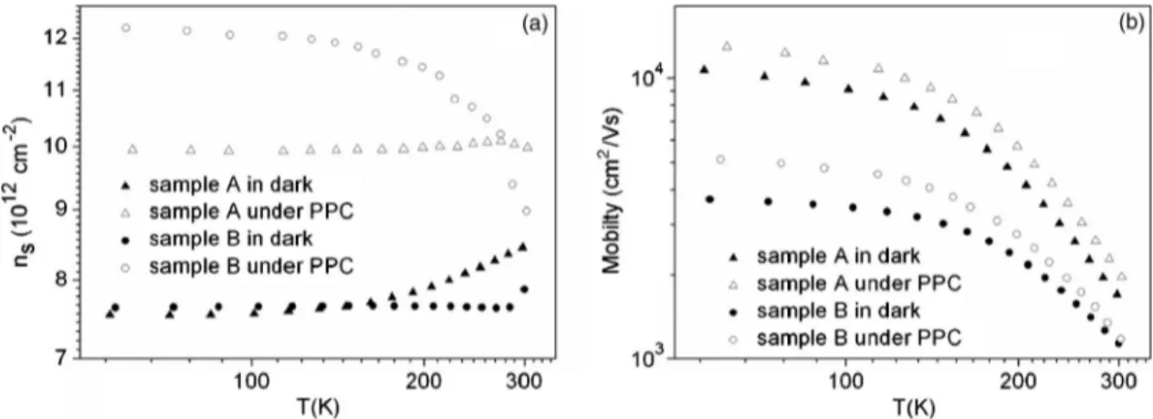
The 2DEG carrier mobilities and carrier concentration behavior for samples A and B were measured in the dark as well as under illumination at different temperatures. The re-sults are shown in Figs.1共a兲and1共b兲. The data for all of the curves shown in Fig.1were collected in the dark. The initial data were collected before the sample was illuminated. Sub-sequently, we exposed the sample to light for 10 min with photon energies of 2.64 eV from the LED. The LED was then turned off and the sample was allowed to stabilize.
insensi-tive to the temperature at low temperature values. This be-havior is typical for the 2DEG. Similar results were observed previously for 2DEG systems in AlGaAs/GaAs共Ref.29兲 and
AlGaN/GaN heterojunctions24,34 in the dark state as well as under illumination. The 2DEG mobility and carrier concen-tration were enhanced significantly for all of the tempera-tures after photoexcitation.10
Figure 1共a兲 shows that the illumination resulted in an increase in the carrier density at all of the temperatures used for both samples. In sample A, the carrier density increased from 7.59⫻1012to 9.93⫻1012 cm−2by way of illumination at 30 K, but in sample B, the increments in the carrier den-sity were larger than those in sample A, in which it increased from 7.62⫻1012 to 1.23⫻1013 cm−2 at the same tempera-ture.
This increment in the carrier density is in agreement with recent PPC reports from other authors.10,24,29 The dif-ference between the increments ratio in both samples comes from the DX center density in the AlGaN layers. The 2DEG mobility increment ratios, due to photoexcitation at a fixed temperature, are different for samples A and B. In fact, at 30 K, it increased from 1.22⫻104 to 1.37⫻104 cm−2/V s for sample A. On the other hand, in sample B, the 2DEG
mobil-ity increments occur from 3.83⫻103 to 5.47
⫻103 cm−2/V s at the same temperature.
One of the dominant scattering mechanisms that limit the mobility of a 2DEG is remote ionized impurity scattering.7–9,29,35,36The increments in mobility due to pho-toexcitation at a fixed temperature can be attributed to the increased electron mean energy with an increasing carrier density in the 2DEG channel, which leads to an improved screening and thereby reduced scattering between the 2DEG electrons with the ionized donor impurities.24,29
The PL measurements taken for the Al0.20Ga0.80N/ GaN/sapphire and Al0.20Ga0.80N/GaN/SiC samples at room temperature are shown in Fig. 2. As seen in Fig. 2, the samples show a strong near-band-edge exciton luminescence line around 3.44 and 3.43 eV for samples A and B, respec-tively. The full widths at half maximum of 30 meV for sample A and 35 meV for sample B are comparable to that of the high-quality GaN. The energy position of the excitonic PL band is shifted by ⬃10 meV for Al0.20Ga0.80N/GaN/
sapphire and⬃20 meV for Al0.20Ga0.80N/GaN/SiC toward high energies compared to the position of the respective ex-citons in the nonstressed GaN layers.9 These results show that there are considerable compressive strains that exist in our GaN layers due to the mismatch between the epilayers. In our case, the compressive strains in GaN on sapphire are larger than those in GaN on SiC.11,13
In addition, the broad deep-level emission centered at approximately 2.2 eV that is modulated by the Fabry–Pérot interference fringes was observed. The appearance of the in-terference indicates the smooth surface of the film. PL mea-surements performed on both samples showed a broad yel-low PL spreading from 1.80 to 2.60 eV with a maximum peak at 2.25 eV. The YB PL emission is generally believed to result from nitrogen vacancies and from impurities such as oxygen.3,17,37The ratio of the near-band-edge excitation peak intensity to the deep-level emission peak intensity ratio is equal to 3 and 1.8 for samples Al0.20Ga0.80N/GaN/sapphire and Al0.20Ga0.80N/GaN/SiC, respectively. This result shows that the Al0.20Ga0.80N/GaN/SiC sample contains more defect density than the Al0.20Ga0.80N/GaN/sapphire sample. Broad peaks were observed between 2.65 and 3.25 eV for both samples. These peaks may be related to the acceptor levels. To investigate the energy distribution of the trap levels,
FIG. 1. The measured共a兲 2DEG carrier density ns and共b兲 mobilityin Al0.20Ga0.80N/GaN/sapphire and Al0.20Ga0.80N/GaN/SiC heterostructures as a function of temperature T measured in the dark state and in the PPC sate.
FIG. 2. Room temperature PL spectra of Al0.20Ga0.80N/GaN/sapphire and Al0.20Ga0.80N/GaN/SiC heterostructure samples.
PC spectra were measured for those excitation energies rang-ing from 2.20 to 4.90 eV. Figure 3 shows the resulting PC spectrum of the Al0.20Ga0.80N/GaN heterojunction on sap-phire and on SiC substrate at room temperature. The PC spectrum of both samples exhibited three peaks at the ener-gies of 3.83, 3.44, and 2.60 eV for sample A and 3.83, 3.43, and 2.60 eV for sample B, which correspond to the band gaps of AlGaN and GaN as well as the GaN YB, respec-tively. In Fig.3, the increments in the PC peak intensity of the AlGaN epilayer as a greater number of incident photons were shown. Because the photon hits the surface without any loss and generates a greater number of electron-hole pairs, the light intensity absorbed at the GaN layer is decreased, resulting in low-intensity band-edge and YB peaks. This re-sulted in good agreement with the previous published results.23
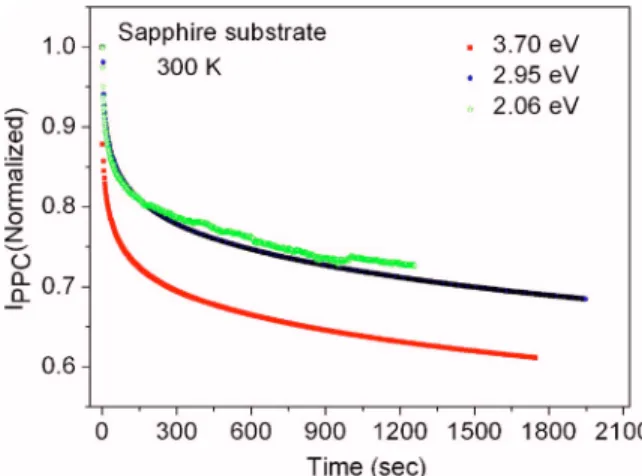
When the Al0.20Ga0.80N/GaN heterojunction samples were illuminated with the photon energies of 2.06, 2.95, and 3.70 eV, PPC was observed in both heterojunctions that were grown on sapphire and SiC substrates. The PPC decay curve samples were normalized to unity at t = 0 according to Ippc共t兲=关I共t兲−Id兴/关I共0兲−Id兴, where I共0兲 is defined as the
cur-rent immediately after the termination of the excitation, I共t兲 as the current at decay time t, and Id as the initial dark
cur-rent共Fig.4兲. The inset in Fig.4shows the PC as a function
of time and illumination in the Al0.20Ga0.80N/GaN/SiC het-erojunction.
Figure5 shows the PPC spectra of sample A as a func-tion of excitafunc-tion photon energy at 300 K. Both of the samples exhibited an initial fast decrease that was then fol-lowed by a slower, but steady, decrement. The rate of the PC decrements changes with the photon energy. Such PPC be-havior has been observed in many III-V and II-VI semicon-ductor thin films and heterostructures.19–26,28,30–32,38–41 The origin of the PPC can be explained by the fact that the pho-toexcited carriers are trapped and spatially separated by local potential fluctuations, which then suppresses the recombina-tion of carriers. The Al content affects the PPC decay rate. Decreasing the Al content causes a faster decay. The carrier transport process can be used for interpreting the slow decay in those samples with high Al compositions. The carrier cap-ture process, from weakly localized states to strongly local-ized states of deeper potential by alloy fluctuations, causes a slow decay in PPC.19,22In addition, the stretched-exponential relaxation is commonly observed in disordered samples.24,31 The persistent increase in the conductivity in the 2DEG channel after the illumination of the PPC in AlGaN/GaN heterostructures can be explained via three possible mecha-nisms. One such mechanism is the photoionization of deep-level donors in the AlGaN barrier. The second is the photo-ionization of deep-level donors in the GaN layer. The last is the electron-hole pair generation in the GaN layer with a subsequent charge separation by the electric field from the macroscopic barrier due to band bending. In order to identify the main mechanism for PPC, we used three different photon energy levels 共2.06, 2.95, and 3.70 eV兲 as illumination sources. Under the excitation with the photon energy condi-tions of q⬍Eg 共2.06 and 2.95 eV兲 of GaN, the energy of
the excitation photons was insufficiently large to generate electron-hole pairs in the GaN layer. For the case of q ⬍Eg共3.70 eV兲 of GaN, in addition to the photoexcitation of
deep-level impurities, band-to-band excitation also generates electron-hole pairs in the GaN layer.
In order to determine the origin of the PPC in Al0.20Ga0.80N/GaN heterostructures, we also performed comparison measurements on the GaN epilayers. For these
FIG. 3. Photoconductivity spectrum of Al0.20Ga0.80N/GaN/sapphire and Al0.20Ga0.80N/GaN/SiC heterostructure samples taken at room temperature.
FIG. 4. Room temperature PPC decay kinetics of the Al0.20Ga0.80N/ GaN/SiC heterostructure.
FIG. 5. 共Color online兲 Room temperature PPC decay kinetics of the Al0.20Ga0.80N/GaN/sapphire heterostructure as a function of excitation energy.
measurements, the AlGaN/AlN layers were etched from the Al0.20Ga0.80N/GaN/sapphire and Al0.20Ga0.80N/GaN/SiC heterojunction samples, in which the PPC effect was absent in the GaN epilayers. In this case, the second mechanism can be precluded for our Al0.20Ga0.80N/GaN heterostructures. These results suggest that the carrier density in the 2DEG channel is primarily contributed by the transfer of photoex-cited electrons from the deep-level impurities 共or DX cen-ters兲 in the AlxGa1−xN/AlN barrier layer.29 Because of the thin AlN interfacial layer, deep-level impurities in the AlxGa1−xN layer may be responsible for the PPC response. These deep levels can be compared to the DX centers in the AlxGa1−xAs layers.17
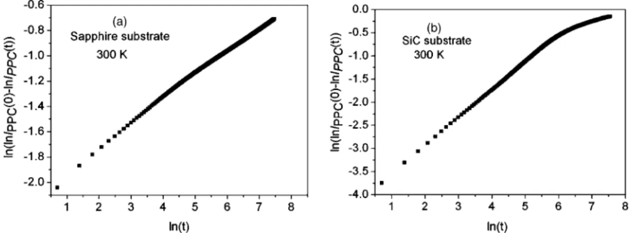
The decay kinetics in PC after turning off the illumina-tion can be described well by a stretched-exponential function,37
IPPC共t兲 = IPPC共0兲 exp关− 共t/兲兴 共0 ⬍⬍ 1兲, 共1兲 where IPPC共0兲 is the initial PC value,is the PPC decay time constant, and  is the decay exponent. This was demon-strated by plotting ln关ln IPPC共0兲−ln IPPC共t兲兴 versus ln共t兲 for the PPC decay curves. Figures 6共a兲and 6共b兲 show a repre-sentative plot of ln关ln IPPC共0兲−ln I共t兲兴 versus ln共t兲 for samples A and B at 300 K. The solid line is the least-squares fit of data with Eq. 共1兲 for the PPC decay. The good linear
behavior that was observed is shown in Fig. 5. The linear behavior of the plot demonstrates that PPC decay can be described well by Eq. 共1兲. The stretched-exponential
relax-ation is commonly observed in disordered
systems,26,28,30,33,37,40,41 which implies that the origin of the observed PPC effect has a similar property. A least-squares fit to the experimental data yields a time constant and de-cay exponentvalues.
The fitted parameters for the PPC decay were = 8.8 ⫻104 s,= 0.25 for sample A and = 1.9⫻103 s,= 0.43 for sample B at 300 K, respectively. The time constant 共兲 and  that was found for Al0.20Ga0.80N/GaN/sapphire are consistent with the values noted in the literature.24,34 How-ever, the values found for Al0.20Ga0.80N/GaN/sapphire het-erostructures are larger than the given values. The difference between these values results from the compressive strain dif-ference in the GaN layers due to the mismatch between the epilayers.
The temperature-dependence measurements of PPC were studied in order to further investigate the origin of the PPC effect phenomena in AlxGa1−xN/GaN heterostructures. As shown in Fig. 7, the PPC effect strongly depends on the temperature. The decay times of the PC depend on the tem-perature and become longer with a decreasing temtem-perature.
FIG. 6. Plot of ln关ln IPPC共0兲−ln IPPC共t兲兴 vs ln共t兲 for 共a兲 Al0.20Ga0.80N/GaN/sapphire and 共b兲 Al0.20Ga0.80N/GaN/SiC heterostructures at room temperature. The linear curves indicate that PPC decays according to stretched-exponential function.
FIG. 7. 共Color online兲 The PPC decay kinetics of 共a兲 Al0.20Ga0.80N/GaN/sapphire and 共b兲 Al0.20Ga0.80N/GaN/SiC heterostructures as a function of temperature.
The temperature dependence of PPC decay behavior was then fit to a well-known stretched-exponential function.
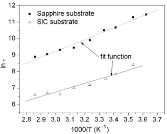
is dependent on temperature. This behavior can be ex-plained as the probability of the thermal activation of the localized carriers to overcome the potential barrier increases by way of increasing temperature. The thermal carriers can escape to the recombination channels. The PPC decay rate, therefore, rapidly increases with increasing temperature. In the thermal activation region, this carrier capture barrier⌬E can be estimated from the temperature dependence of the time constant18
=0exp关⌬E/kT兴, 共2兲
where0 is the high temperature limit of the time constant and⌬E is the activation energy for the thermal capture of an electron at DX-like deep levels. Figure8shows the Arrhen-ius plot ofwith temperature. The resulting energy barriers for the capture of electrons in the 2DEG channel by the deep-level impurities 共DX-like centers兲 in AlGaN for the Al0.20Ga0.80N/GaN/sapphire and Al0.20Ga0.80N/GaN/SiC heterojunction samples are 343 and 228 meV, respectively. The obtained ⌬E value for Al0.20Ga0.80N/GaN/SiC is con-sistent with the previously reported values.34 However, the obtained⌬E value for sample A is larger than that in sample B. This result can be explained by the depth of the localiza-tion in Al0.20Ga0.80N. The depth of the localization is deeper for sample A. The different ranges of localization can be attributed to the effect of the larger cluster size in sample A.25
IV. CONCLUSIONS
We studied the substrate material effects on the electrical and optical properties in AlxGa1−xN/GaN heterostructures 共x=0.20兲. The illumination of the samples with a blue 共 = 470 nm兲 LED induced a persistent increase in the carrier density and 2DEG electron mobility. In agreement with the previously reported PPC results, the PPC effect resulted in an increase in carrier and mobility density. In sample A, the carrier density increased from 7.59⫻1012 to 9.93 ⫻1012 cm−2by illumination at 30 K. On the other hand, in
of the near-band-edge excitation peak intensity to the deep-level emission peak intensity ratio was equal to 3 and 1.8 for samples Al0.20Ga0.80N/GaN/sapphire and Al0.20Ga0.80N/ GaN/SiC, respectively. Both of the samples were illuminated with three different energy photons. We observed different decay rates for three different photon energy levels. These behaviors can usually be attributed to the presence of carrier localization states and are explained based on the alloy com-positional fluctuations in the AlxGa1−xN alloys. The PPC de-cay behavior can be well described by a stretched-exponential function and the relaxation time constant , in which the decay exponentchanges with the substrate ma-terial. The energy barriers for the capture of electrons in the 2DEG channel by the deep-level impurities 共DX-like cen-ters兲 in AlGaN for the Al0.20Ga0.80N/GaN/sapphire and Al0.20Ga0.80N/GaN/SiC heterojunction samples are 343 and 228 meV, respectively. The activation energy for the thermal capture of an electron by defects ⌬E was found to change with the substrate materials. Our results have revealed that the substrate material strongly affects the electrical and opti-cal properties of Al0.20Ga0.80N/GaN heterostructures. These results can be explained with the differing degrees of lattice mismatch between the grown layers and substrates.
ACKNOWLEDGMENTS
This work was supported by the European Union under the Project Nos. METAMORPHOSE and EU-NoE-PHOREMOST and TUBITAK under the Project Nos. 105E066, 105A005, 106E198, and 106A017. One of the au-thors 共E.O.兲 also acknowledges partial support from the Turkish Academy of Sciences.
1S. N. Mohammad, A. Salvador, and H. Morkoç, Proc. IEEE 83, 1420 共1996兲.
2L. Shen, S. Heikman, B. Moran, R. Coffie, N.-Q. Zhang, D. Buttari, I. P. Smorchkova, S. Keller, S. P. DenBaars, and U. K. Mishra,IEEE Electron Device Lett.22, 457共2001兲.
3S. Butun, M. Gokkavas, H. Yu, and E. Ozbay, Appl. Phys. Lett.89, 073503共2006兲.
4T. Tut, M. Gokkavas, B. Butun, S. Butun, E. Ulker, and E. Ozbay,Appl. Phys. Lett.89, 183524共2006兲.
5S. Nakamura, M. Senoh, S. Nagahama, N. Iwasa, T. Yamada, T. H. Kiy-oku, Y. Sugimoto, T. Kozaki, H. Umemoto, M. Sano, and K. Chocho, Appl. Phys. Lett. 72, 1687共1998兲.
6A. Y. Polyakov, N. B. Smirnov, A. S. Usikov, A. V. Govorkov, and B. V. Pushniy,Solid-State Electron.42, 627共1998兲.
7L. Hsu and W. Walukiewicz,Phys. Rev. B56, 1520共1997兲.
8T. Wang, Y. Ohno, M. Lacha, D. Nakagawa, T. Shirahama, S. Sakai, and H. Ohno,Appl. Phys. Lett.74, 3531共1999兲.
FIG. 8. Arrhenius plot of PPC decay time constant共vs 1000/T兲 in the Al0.20Ga0.80N/GaN/sapphire and Al0.20Ga0.80N/GaN/SiC heterostructure samples.
9M. Redwing, M. A. Tischler, J. S. Flynn, S. Elhamri, M. Ahoujja, and R. S. W. C. Mitchel,Appl. Phys. Lett.69, 963共1996兲.
10N. Biyikli, Ü. Özgür, X. Ni, Y. Fu, H. Morkoç, and Ç. Kurdak,J. Appl. Phys.100, 103702共2006兲.
11H. Yu, D. Caliskan, and E. Ozbay,J. Appl. Phys.100, 033501共2006兲. 12R. Gaska, J. W. Yang, A. Osinsky, Q. Chen, M. Asif Khan, A. O. Orlov,
G. L. Snider, and M. S. Shur,Appl. Phys. Lett.72, 707共1998兲.
13A. Dadgar, C. Hums, A. Diez, J. Bläsing, and A. Krost,J. Cryst. Growth
297, 279共2006兲.
14X. Z. Dang, C. D. Wang, E. T. Yu, K. S. Boutrous, and J. M. Redwing, Appl. Phys. Lett.72, 2745共1998兲.
15C. H. Qiu, C. Hoggatt, W. Melton, M. W. Leksono, and J. I. Pankove, Appl. Phys. Lett.66, 2712共1995兲.
16H. X. Jiang and J. Y. Lin,Phys. Rev. B40, 10025共1989兲.
17D. V. Lang, R. A. Logan, and M. Joros,Phys. Rev. B19, 1015共1979兲. 18H. J. Queisser and D. E. Theodorou,Phys. Rev. B33, 4027共1986兲. 19N. Sarkar, S. Dhar, and S. Ghosh,J. Phys.: Condens. Matter15, 7325
共2003兲.
20M. A. Reshchikov, G.-C. Yi, and B. W. Wessels,Phys. Rev. B59, 13176 共1999兲.
21J. Z. Li, J. Y. Lin, H. X. Jiang, A. Salvador, A. Botchkarev, and H. Morkoc,Appl. Phys. Lett.69, 1474共1996兲.
22S. J. Chung, B. Karunagaran, S. Velumani, C.-H. Hong, H. J. Lee, and E.-K. Suh,Appl. Phys. A: Mater. Sci. Process.86, 521共2007兲.
23X. Z. Dang, C. D. Wang, E. T. Yu, K. S. Boutros, and J. M. Redwing, Appl. Phys. Lett.72, 2745共1998兲.
24J. Z. Li, J. Y. Lin, H. X. Jiang, M. Asif Khan, and Q. Chen,J. Appl. Phys.
82, 1227共1997兲.
25S. J. Chung, M. Senthil Kumar, H. J. Lee, and E.-K. Suh,J. Appl. Phys.
95, 3565共2004兲.
26K. C. Zeng, J. Y. Lin, and H. X. Jiang,Appl. Phys. Lett.76, 1728共2000兲. 27A. Dissanayake, M. Elahi, H. X. Jiang, and J. Y. Lin,Phys. Rev. B45,
13996共1992兲.
28K. C. Zeng, J. Y. Lin, and H. X. Jiang,Appl. Phys. Lett.76, 1728共2000兲. 29Z. Peng, T. Saku, and Y. Horikoshi,J. Appl. Phys.79, 3592共1996兲. 30T. Y. Lin, H. M. Chen, M. S. Tsai, Y. F. Chen, F. F. Fang, C. F. Lin, and G.
C. Chi,Phys. Rev. B58, 13793共1998兲.
31H. M. Chen, Y. F. Chen, M. C. Lee, and M. S. Feng,J. Appl. Phys.82, 899 共1997兲.
32S. J. Chung, M. Senthil Kumar, Y. K. Kim, C.-H. Hong, H. J. Lee, and E.-K. Suh, J. Korean Phys. Soc. 45, 1279共2004兲.
33C. Wetzel, T. Suski, J. W. Ager, E. R. Weber, S. Fischer, B. K. Meyer, R. J. Molnar, and P. Perlin,Phys. Rev. Lett.78, 3923共1997兲.
34J. Z. Li, J. Y. Lin, H. X. Jiang, M. A. Khan, and Q. Chen,J. Vac. Sci. Technol. B15, 1117共1997兲.
35M. N. Gurusinghe, S. K. Davidsson, and T. G. Andersson,Phys. Rev. B
72, 045316共2005兲.
36J. Antoszewski, M. Gracey, J. M. Dell, L. Faraone, T. A. Fisher, G. Parish, Y.-F. Wu, and U. K. Mishra,J. Appl. Phys.87, 3900共2000兲.
37S. J. Chung, O. H. Cha, Y. S. Kim, M. S. Jeong, C.-H. Hong, H. J. Lee, M. S. Jeong, J. O. White, and E.-K. Suh,J. Appl. Phys.89, 5454共2001兲.
38T. Y. Lin, H. C. Yang, and Y. F. Chen,J. Appl. Phys.87, 3404共2000兲. 39C. H. Qiu and J. I. Pankove,Appl. Phys. Lett.70, 1983共1997兲. 40L. H. Chu, Y. F. Chen, D. C. Chang, and C. Y. Chang,J. Phys.: Condens.
Matter7, 4525共1995兲.
41C. Johnson, J. Y. Lin, H. X. Jiang, M. A. Khan, and C. J. Sun,Appl. Phys. Lett.68, 1808共1996兲.