Ankara University
Institute of Nuclear Sciences
Owner on behalf of Institute of Nuclear Sciences,
Ankara University,
Director
Niyazi MERİÇ, Ph.D.
http://jns.ankara.edu.tr
Editor-in-Chief
Haluk YÜCEL, Ph.D.
Assistant Editor-in-Chief
George S. POLYMERIS, Ph.D.
Editorial Board
Birol ENGİN, Ph.D.
Erkan İBİŞ, M.D.
Gaye Ö. ÇAKAL, Ph.D.
Güneş TANIR, Ph.D.
Hamit HANCI, M.D.
Ioannis LIRITZIS, Ph.D.
İsmail BOZTOSUN, Ph.D.
M.Salem BADAWI, Ph.D.
Mustafa KARADAĞ, Ph.D.
Niyazi MERİÇ, Ph.D.
Osman YILMAZ, Ph.D.
Özlem BİRGÜL, Ph.D.
Özlem KÜÇÜK, M.D.
Slobodan JOVANOVIC, Ph.D.
Turan OLĞAR, Ph.D.
Volume 2, No. 2
May 2015
ISSN: 2148-3981
Journal of Nuclear Sciences
Not for reproduction, distribution or commercial use.
Provided for non-commercial research and education use.
* Corresponding author.
E-mail address: [email protected] (Ş. Kaya). Journal of Nuclear Sciences, Vol. 2, No. 2, May 2015, 48-52 Copyright © Ankara University Institute of Nuclear Sciences ISSN: 2147-7736
Journal of Nuclear Sciences
ISSN: 2147-7736
J o ur na l h om e page: h t tp :/ / j n s . a n k a r a . e d u . t r /
DOI: 10.1501/nuclear_0000000012
Influences of irradiation on the C–V and G/ ω –V characteristics of Si
3N
4MIS capacitors
Ş. Kaya
1,2,*, E. Yılmaz
1,2and A.O. Çetinkaya
1,21Physics Department, Abant Izzet Baysal University, 14280 Bolu, Turkey 2Center for Nuclear Radiation Detector Research and Applications, 14280 Bolu, Turkey
Received 14.11.2014; received in revised form 03.02.2015; accepted 18.04.2015
ABSTRACT
The effects of gamma-ray exposures on the electrical characteristics of Silicon Nitride (Si3N4) metal–insulator–
semiconductor (MIS) structures have been investigated at room temperature. The MIS structures were irradiated with the GAMMACELL 220 Co-60 radioactive source. The distributions of interface states and series resistance were determined from the C–V and G/ω-V characteristics by taking into account the irradiation-dependent the barrier height. Both the values of series resistance, interface states and barrier heights enhanced with increasing dose. Experimental results demonstrate that gamma-ray irradiations have the significant effects on electrical characteristics of Si3N4 MIS structures.
Keywords: Radiation effects, Si3N4 MIS capacitor, Interface states, Series resistance.
1. Introduction
Metal Insulator Semiconductors (MIS) are
technologically important devices that have many
electronic applications such as transistors,
photovoltaic, radiation sensors etc. The suitability and usability of MIS devices in technological applications depends on the device characteristics, which are directly related to the gate insulators and their interfaces with the underlying semiconductors [1]. Owing to several possible sources of errors, the electrical characteristics of MIS capacitors deviate from their expected ideal behaviors. These errors may be related to such parameters as the interface-state densities (Dit) and series resistances (Rs).
Therefore, these parameters should be taken into account in relevant calculations.
On the other hand, semiconductor based devices such as Schottky barrier diodes (SBDs), metal-insulator/oxide-semiconductor (MIS or MOS) structures and solar cells have been used in many satellites and played important roles in a wide range of communications, broadcast, meteorological, scientific research, space development applications and other industrial areas. Development of electronic sensors, MS or MIS structures with
stable performance in strongly ionizing radiation fields is also essential to improving the reliability of atomic power plants and nuclear fusion systems [2]. It is well known that MIS devices are extremely sensitive to ionizing radiation, and the radiation response of these devices has been found to change significantly due to the variations on the Dit and Rs.
However it has been reported that the radiation induced flat- band voltage shift of the nitride based structure is smaller than that of the MOS/MIS structure, and the radiation hardness has been improved [3, 4]. Silicon nitride (Si3N4) is one of the
promising nitride films with high dielectric constant low surface state density and thermal stability underlying silicon substrate [1, 5, 6]. Therefore, the purpose of the present work is to investigate effects of irradiation on Si3N4 MIS devices. In order to
investigate influences of irradiation on these electrical characteristics of Si3N4 MIS capacitors,
the samples were irradiated by using the Co-60
gamma ray source from 5 Gy to 10 Gy. The
electrical characteristics of the device were investigated from high frequency (1 MHz) C-V and
Kaya et.al/Journal of Nuclear Sciences Vol 2(2) (2015) 48-52
49 G/ω-V measurements and discussed for different exposure doses.
2. Experimental
Silicon nitride (Si3N4) films with a thickness of 100
nm were deposited by plasma enhanced chemical vapor deposition (PECVD) at 13.56MHz on p-type (100) Si substrate using a gas mixture of ammonia
(NH3) and silane (SiH4). The plasma power and
growth temperature were fixed at 10 W and 250 0C,
respectively. The pressure in the chamber remained at 500 mTorr. To study the response of MIS devices to irradiation over a range of doses, MIS samples were irradiated using a Co-60 gamma-ray source for 5 Gy and 10 Gy. Capacitance-voltage (C-V) and conductance-voltage (G/ω-V) measurements were performed at high frequency (1 MHz) before and after gamma irradiation by using an Impedance Analyzer in dark environment at room temperature.
3. Results and Discussion
Fig. 1 demonstrates the C-V characteristics of Si3N4
MIS capacitor under different irradiation doses. The fabricated devices exhibit characteristic MIS type behavior with three known distinct regimes as accumulation, depletion and inversion for all measurements. Ionizing radiation such as gamma rays and X-rays generates defects, interface trap and oxide trap-charges in MIS structure [7]. Hence, ionizing radiation causes a shift in flat band and mid-gap voltage. The shifts of the C-V curves are to the left side after irradiation as seen in Fig. 1. The behaviors of capacitances can be caused by the enhancement of trapped charge densities such as interface trapped charges and oxide trapped charge in MIS device generated by irradiation [8, 9]. In addition, the measured capacitances slightly decrease with increasing irradiation doses and this may be due to series resistance, contribution of interface states capacitance generated by irradiation to measured capacitance and/or the leakage through the oxide is responsible for the slight decrease of the C–V curves in accumulation region [10, 11]. -24 -21 -18 -15 -12 4,0x10⁻¹⁰ 6,0x10⁻¹⁰ 8,0x10⁻¹⁰ 1,0x10⁻⁹ 1,2x10⁻⁹ Capac itanc e (F ) Voltage (V) Non- Irrad. 5 Gy 10 Gy
Fig.1. The measured C–V curves of Si3N4 MIS
capacitor before and after gamma radiation at different doses.
Fig. 2 shows the G/ω-V characteristics of Si3N4
MIS capacitor under different irradiation doses. The conductance method [12, 13] is based on the conductance losses resulting from the exchange of majority carriers and the interface states when a small voltage signal is applied to the MIS devices. Therefore they are important characteristics in order to determine the interface defects distributions of MIS devices. As seen in Fig. 2, the conductance
characteristics decrease whole regions with
increasing the irradiation doses, indicating that variations of the lattice defects in the form of vacancies, defect clusters in the interface between insulator and semiconductor layers [14]. In addition the voltage shifts toward negative voltage axis with increasing irradiation dose were observed from Fig. 2. This behavior may be related to the changes in the distribution of interface states, and series resistance characteristics of devices.
-24 -21 -18 -15 -12 1,30x10⁻¹⁰ 1,95x10⁻¹⁰ 2,60x10⁻¹⁰ 3,25x10⁻¹⁰ 3,90x10⁻¹⁰ 4,55x10⁻¹⁰ G/ (F ) Voltage (V) Non- Irrad. 5 Gy 10 Gy
Fig.2. The measured G/ω-V curves of Si3N4 MIS
capacitor before and after gamma radiation at different doses.
The real series resistances of the MIS structure can be calculated from the measured capacitance (Cma)
and conductance (Gma) in the strong accumulation
region at high frequencies [5, 12, 15]:
2 ma 2 ma ma s ) C ( ) G ( G R (1)
where ω is the angular frequency, and Cma and Gma
are defined as the measured capacitance and conductance in the strong accumulation region,
respectively. Calculated Rs values are given in
Table 1 and slightly rise in the Rs values with
increasing irradiation dose have been observed, due to the reordering and restructuring of radiation-induced defects in the MIS capacitors. These
obtained Rs values were used to correct the
measured G/ω-V and C-V characteristics of the devices.
In order to remove the effects of Rs on the measured
capacitance (Cm) and conductance (Gm)
characteristics and evaluate the real interface trap density Dit of Si3N4 MIS device before and after
irradiation, C–V and G/ω–V curves were corrected
by the obtained Rs values. The corrected
capacitance Cc and conductance Gc were calculated
from following equations [5, 12, 15]:
2 m 2 2 m 2 m c ) C ( a ] ) C ( ) G [( C Cm (2) and 2 2 2 2
)
(
]a
)
(
)
[(
m m m cC
a
C
G
G
(3) Where s 2 2 m m) [(G ) ( ) ]R G ( a Cm , ω is theangular frequency, (2πƒ), Gm and Cm are measured
conductance and capacitance, respectively. The distributions of Cc and Gc/ω as a function biases are
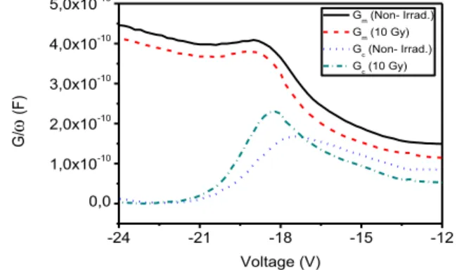
seen in Fig. 3 (a) and (b) before and after irradiation, respectively. These figures show the
corrected conductance and capacitance
characteristics have significant change compared to the measured values. Capacitance increases while conductance decreases after corrections. These behaviors demonstrate that the series resistances
were masking the real C-V and G/ω-V
characteristics and the peaks in the corresponding depletion edge give an evidence on the interaction between interface states and majority carriers of semiconductors [15, 16]. -24 -21 -18 -15 -12 4,0x10⁻¹⁰ 6,0x10⁻¹⁰ 8,0x10⁻¹⁰ 1,0x10⁻⁹ 1,2x10⁻⁹ 1,4x10⁻⁹ Capac itanc e (F ) Voltage (V) Cm (Non- Irrad.) Cm (10 Gy) Cc (Non- Irrad.) Cc (10 Gy)
Fig.3.(a) The correction effects on the C-V
characteristics of Si3N4 MIS capacitors.
-24 -21 -18 -15 -12 0,0 1,0x10⁻¹⁰ 2,0x10⁻¹⁰ 3,0x10⁻¹⁰ 4,0x10⁻¹⁰ 5,0x10⁻¹⁰ G/ (F ) Voltage (V) Gm (Non- Irrad.) Gm (10 Gy) Gc (Non- Irrad.) Gc (10 Gy)
Fig.3.(b) The correction effects on the G/ω-V
characteristics of Si3N4 MIS capacitors.
It is well-known that the distributions of interface states are important parameter to examine effects of radiation on MIS structures. Several suggested methods [7, 9, 11] can be used to determine Dit.
Among these, Hill-Coleman method [17] is fast and reliable one in order to determine the density of interface states. Thus, Dit can be calculated by Eq.
4: 2 ox c 2 ox max , c max , c it ) C / C 1 ( ) C / G ( / G Aq 2 D (4)
where, q is the electrical charge, A is the front
contact area MIS capacitor, Cox is the capacitance of
oxide layer in accumulation region of Cc–V curve
for non-irradiated devices, Gc,max/ω is peak values
of corrected G/ω–V curve, Cc is corrected
capacitance of the MIS capacitor corresponding to
Gc,max/ω. The densities of interface states calculated
by using Eq. 4 prior to and after irradiation were given in Table 1. It is seen that Dit values increase
with increasing in irradiation dose. This is due to the increasing in defects concentrations on MIS devices by irradiation. However, the calculated Dit
values of MIS devices are about order of 1012 eV-1
cm-1. This order of Dit values is not high enough to
pin Fermi level of Si substrate corrupting device operation.
Table 1. Some electrical characteristics of Si3N4 MIS devices under irradiation.
Dose (Gy) Rs (Ohm) Gc max x 10-10 (F) Cc x 10-10 (F) Dit x 1012 (eV-1cm-2) VD (eV) φB (eV) 0 414 1.68 8.04 1.44 19.1 19.0 5 421 1.91 8.15 1.65 19.8 19.6 10 435 2.31 7.91 1.77 21.3 21.1
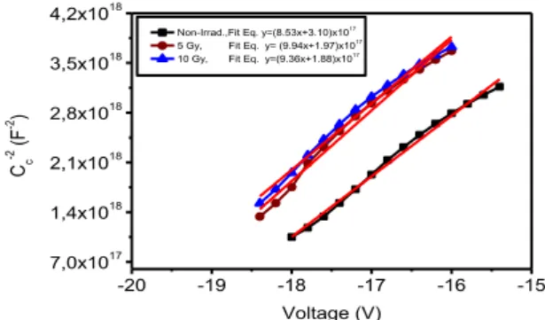
Kaya et.al/Journal of Nuclear Sciences Vol 2(2) (2015) 48-52 51 -20 -19 -18 -17 -16 -15 7,0x10¹⁷ 1,4x10¹⁸ 2,1x10¹⁸ 2,8x10¹⁸ 3,5x10¹⁸ 4,2x10¹⁸ Cc -2 (F -2 ) Voltage (V) Non-Irrad.,Fit Eq. y=(8.53x+3.10)x1017
5 Gy, Fit Eq. y= (9.94x+1.97)x1017
10 Gy, Fit Eq. y=(9.36x+1.88)x1017
Fig. 4. The Cc
-2–V characteristics for the Si
3N4MIS
capacitor before and after gamma irradiation. The irradiation dependent barrier height (
B
) ofdevices can be calculated from reverse voltage Cc-2
–V characteristics seen in Fig. 4 by following the relation [1, 12, 18]: B a V D B F 0 B N N ln q kT V E q kT V (5)
where EF is the energy difference between the bulk
Fermi level and valance band edge, NV is the
effective density of states in valance band. V0 (=
VD- kT/q) is the intercept of the Cc -2
vs. V plot with
the voltage axis prior to and after irradiation, VD is
the diffusion potential and
B
is the image forcebarrier lowering and can be calculated from the following Eq.6 [1]: 0 s m B 4 qE (6)
where Em 2qVDNa/0s is the maximum
electric field detailed in literature [19]. The intercept of Cc-2 vs. V plot calculated from linear fit
equation of Cc
-2
vs. V in Fig. 4, is negative voltage value for non-irradiated sample which indicates that a fairly large number of positive charges are trapped in devices structure due to fabrication process. In addition, the calculated barrier heights respect to radiation doses are tabulated in Table 1. The increases in barrier height have been observed.
This is due to an increase in diffusion potential, Vd.
Devices had wide-barrier height decrease charge injection from the substrate into the dielectric and thus the tunneling effects into the structure may decrease resulting from higher value of barrier height.
4. Conclusion
The variations in the measured C-V and G/ω-V characteristics have been observed after irradiation, owing to generated defect densities and trapped charges in the device structure. In addition, the real
conductance values increase with increasing the radiation dose, while the experimental conductance value decrease with increasing radiation dose and the corrected capacitance is also different from experimental measurements. These obtained results demonstrate that the series resistance is a crucial
factor which can mask the real device
characteristics for device behavior. Additionally, the barrier heights of devices increase with increasing the irradiation and this behavior may be attributed the changes in diffusion potential.
Acknowledgement
This work is supported by Ministry of Development of Turkey under Contract Number: 2012K120360
and was partially presented in 8th International
Conference on Luminescence and ESR Dosimetry (LUMIDOZ 8).
5. References
[1] S. Zeyrek, A. Turan, M.M. Bulbul, "The C-V and G/omega-V Electrical Characteristics of Co-60
gamma-Ray Irradiated Al/Si3N4/p-Si (MIS)
Structures", Chinese Phys Lett, 30 (2013).
[2] H. Uslu, M. Yildirim, S. Altindal, P. Durmus, "The effect of gamma irradiation on electrical and dielectric properties of organic-based Schottky barrier diodes (SBDs) at room temperature", Radiat Phys Chem, 81 362-369 (2012).
[3] H.L. Hughes, J.M. Benedetto, "Radiation effects and hardening of MOS technology: Devices and circuits", IEEE T Nucl Sci, 50 500-521 (2003). [4] K. Watanabe, M. Kato, T. Okabe, M. Nagata, "Radiation Effects of Double-Layer Dielectric Films", IEEE T Nucl Sci, 33 1216-1222 (1986). [5] M.M. Bulbul, S. Zeyrek, S. Altindal, H. Yuzer, "On the profile of temperature dependent series resistance in Al/Si3N4/p-Si (MIS) Schottky diodes",
Microelectron Eng, 83 577-581 (2006).
[6] X.J. Liu, J.J. Zhang, X.W. Sun, Y.B. Pan, L.P. Huang, C.Y. Jin, "Growth and properties of silicon nitride films prepared by low pressure chemical
vapor deposition using trichlorosilane and
ammonia", Thin Solid Films, 460 72-77 (2004). [7] T.P. Ma, P.V. Dressendorfer, "Ionizing Radiation Effects in MOS Devices and Circuits", Wiley & Sons, (1989).
[8] F.B. Ergin, R. Turan, S.T. Shishiyanu, E.
Yilmaz, "Effect of gamma-radiation on HfO2 based
MOS capacitor", Nucl Instrum Meth B, 268 1482-1485 (2010).
52 [9] E. Tugay, E. Yilmaz, R. Turan, "Influence of gamma irradiation on the C-V characteristics of the Al/SiNx/Si MIS capacitors", J Vac Sci Technol A,
30 (2012).
[10] V. Singh, N. Shashank, S.K. Sharma, R.S. Shekhawat, D. Kumar, R.K. Nahar, "Frequency dependence studies on the interface trap density and series resistance of HfO2 gate dielectric deposited
on Si substrate: Before and after 50 MeV Li3+ ions
irradiation", Nucl Instrum Meth B, 269 2765-2770 (2011).
[11] N. Tugluoglu, "Co-60 gamma-ray irradiation effects on the interface traps density of tin oxide films of different thicknesses on n-type Si (111) substrates", Nucl Instrum Meth B, 254 118-124 (2007).
[12] E.H. Nicollian, J.R. Brews, "MOS (Metal Oxide Semiconductor) Physics and Technology", Wiley & Sons, (2003).
[13] P. Chattopadhyay, A.N. Daw, "On the Current
Transport Mechanism in a Metal-Insulator
Semiconductor (MIS) Diode", Solid State Electron, 29 555-560 (1986).
[14] A. Tataroglu, S. Altindal, "Gamma-ray irradiation effects on the interface states of MIS
structures", Sensor Actuat a-Phys, 151 168-172 (2009).
[15] S. Kaya, A. Aktag, E. Yilmaz, "Effects of gamma-ray irradiation on interface states and
series-resistance characteristics of BiFeO3 MOS
capacitors", Nucl Instrum Meth B, 319 44-47 (2014).
[16] S. Kaya, R. Lok, A. Aktag, J. Seidel, E.
Yilmaz, "Frequency dependent electrical
characteristics of BiFeO3 MOS capacitors", J Alloy
Compd, 583 476-480 (2014).
[17] W.A. Hill, C.C. Coleman, "A
Single-Frequency Approximation for Interface-State
Density Determination", Solid State Electron, 23 987-993 (1980).
[18] A. Tataroglu, S. Altindal, "Characterization of interface states at Au/SnO2/n-Si (MOS) structures",
Vacuum, 82 1203-1207 (2008).
[19] A. Kinoshita, M. Iwami, K. Kobayashi, I. Nakano, R. Tanaka, T. Kamiya, A. Ohi, T. Ohshima, Y. Fukushima, "Radiation effect on pn-SiC diode as a detector", Nucl Instrum Meth A, 541 213-220 (2005).