Broadband Optical Modulators Based on Graphene Supercapacitors
Emre O. Polat and Coskun Kocabas*
Department of Physics, Bilkent University, 06800, Ankara, Turkey
*
S Supporting InformationABSTRACT: Optical modulators are commonly used in communication and information technology to control intensity, phase, or polarization of light. Electro-optic, electroabsorption, and acousto-optic modulators based on semiconductors and compound semiconductors have been used to control the intensity of light. Because of gate tunable optical properties, graphene introduces new potentials for optical modulators. The operation wavelength of graphene-based modulators, however, is limited to infrared wavelengths due to inefficient gating schemes. Here, we report a broadband optical modulator based on
graphene supercapacitors formed by graphene electrodes and electrolyte medium. The transparent supercapacitor structure allows us to modulate optical transmission over a broad range of wavelengths from 450 nm to 2μm under ambient conditions. We also provide various device geometries including multilayer graphene electrodes and reflection type device geometries that provide modulation of 35%. The graphene supercapacitor structure together with the high-modulation efficiency can enable various active devices ranging from plasmonics to optoelectronics.
KEYWORDS: Graphene, optical modulator, supercapacitor, optoelectronics
M
onoatomic thickness, optical transparency, andbroad-band absorption of graphene together with gate-tunable carrier density provide unique platform for electro-optical devices.1−5 Graphene interacts with light through interband and intraband electronic transitions.4 Optical response of graphene at visible and near-infrared frequencies is defined by interband transition where the momentum of light is not
sufficient to create electron−hole pair in the same band.
Because of the linear band structure of the graphene, the interband transitions yield broadband optical response with constant optical conductivity6 (σ = πe2/2h). At long wave-lengths (far-infrared and terahertz frequencies), the interband transitions are blocked due to unintentional doping, therefore the optical response is dominated by the low energy intraband transition. These transitions yield gate-tunable Drude-like optical conductivities7 (σ(ω) = σDC/(1−iωτ), where σDC is the low frequency conductivity, ω is the angular frequency of light, and τ is the electron scattering time). Active optical devices such as detectors,8 modulators,5,9 tunable antennas,10 and meta-materials11 working at far-infrared and terahertz wavelengths have been demonstrated based on gate-tunable intraband transition.
Controlling interband transitions of graphene in the visible and near-infrared wavelength, however, requires much higher carrier concentrations.12 By electrical tuning of the Fermi energy (EF), the interband transition with energies less than | 2EF| can be blocked due to Pauli blocking resulting transparent
graphene. Liu et. al13 demonstrated an electroabsorption
modulator using graphene integrated on an optical waveguide working at near-infrared (NIR) wavelengths. In their work, the Fermi energy of graphene is tuned up to 0.5 eV through a
dielectric capacitor. Similar device structures, usually back-gated transistors, have been implemented to tune photonic and plasmonic cavities operating at NIR. The electrical breakdown of the dielectric layer of the capacitor limits the operation in the visible and NIR spectra. The working wavelength can be reduced down to 700 nm by electrolyte gating of graphene layer.12,14,15In the electrolyte gating schemes, application of a gate voltage polarizes the electrolyte and forms an electrical double layer (EDL) near the graphene surface. Since the thickness of EDL is around a few nanometer, EDL generates very large electric fields and associated Fermi energies. The electrochemical potential window of the electrolyte limits the maximum bias voltage and the carrier concentration.
As an alternative gating scheme, we propose to use supercapacitors instead of dielectric capacitors. Supercapacitors, also called ultracapacitor or electric double-layer capacitors, store charges at the electric double-layers formed at the electrolyte−electrode interface. Carbon-based electrodes pro-vides very large surface area that enhances energy storage capacity.16−18Recent studies indicate that graphene electrodes provide scalable approach for ultrahigh energy densities.16−18 Here, we report uses of graphene supercapacitors as broadband optical modulators. The proposed device consists of two parallel graphene electrodes and electrolyte between them. The modulator has simple parallel plate geometry, yet, with a very
efficient device operation. The graphene supercapacitors
operate as electroabsorption modulators over a broad range
Received: July 16, 2013 Revised: October 20, 2013 Published: November 11, 2013
Letter
of wavelengths from 450 nm to 2 μm under ambient conditions. We also studied various device geometries to increase the modulation amplitude. We were able to obtain modulation of 35% using a few layer graphene with an ionic liquid electrolyte.
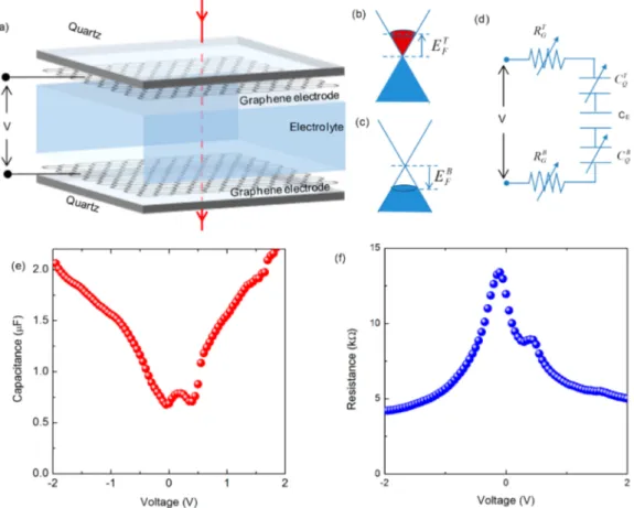
Figure 1a shows the schematic drawing of the graphene capacitor used as an optical modulator. We transferred large area graphene layers on double-side-polished quartz wafers (1 × 2 cm graphene layers are grown by chemical vapor deposition on copper foils, Supporting Information Figure S1). Graphene-coated quartz wafers were put together by a 100 μm thick spacer. The gap between the graphene electrodes werefilled with an electrolyte solution. We used 5 mM solution
of tetrabutylammonium tetrafluoroborate (TBA BF4) in DI
water as the electrolyte because of its large electrochemical potential window. Application of a voltage bias between the top and bottom graphene electrodes polarizes the electrolyte and generates double layer formation at the interface of graphene electrodes with different polarities. The double layers with different polarities electrostatically dope the graphene electro-des and shift the Fermi energy of graphene electroelectro-des in the opposite directions. The schematic band structure of the top and bottom graphene electrodes are shown in Figure 1b,c. Unlike dielectric capacitors where the voltage drops linearly between the electrodes, in supercapacitors the voltage drops sharply at the double layers (in a few nanometers), which generates very large electricfields.
The equivalent circuit of the graphene-supercapacitor is shown in Figure 1d. Superscript“T” and “B” represent the top and bottom electrodes, respectively. In the circuit, the arrows represent the voltage dependent circuit elements. The charge density of graphene layers defines the resistance (RGT,RGB) and the quantum capacitance (CQT,CQB) of electrodes. At room
temperature, the quantum capacitance19 of graphene is
expressed as20,21 CQ = e2D = (2e2/ℏνF)(n/π)1/2 where D is the density of states,n is the charge concentration and vFis the Fermi velocity. CE represents the electrostatic capacitance of the double layers. We measured the value ofCEas 30−40 μF/ cm2(Supporting Information, Figure S2) which is much larger than the quantum capacitance of the graphene electrodes at low
doping concentrations (2 μF/cm2). Therefore, the total
capacitance of the optical modulator is limited by the quantum capacitance of the electrodes (for capacitors connected in series; the equivalent of the circuit is defined by the smallest capacitance). At high carrier concentrations, the quantum capacitance of the graphene electrodes increases up to 20μF/ cm2and becomes comparable with the capacitance of the ionic double (Supporting Information, Figure S3). This causes flattening of the total capacitance at high carrier concentrations. To extract the voltage dependence of the circuit elements (quantum capacitance and resistance of graphene electrodes), we measured the impedance of the graphene supercapacitor as a function of bias voltage. We used an excitation signal of 100 mV at 20 Hz and measured the phase and amplitude of the generated alternating current through the capacitor. Figure 1e,f Figure 1.(a) Schematic exploded view of the optically transparent double layer capacitor formed by two parallel graphene electrodes transfer-printed on quartz substrates and the electrolyte medium (5 mM TBA BF salt in DI water) between them. (b,c) Schematic representation of the electronic band structure of the top and bottom graphene layers under a voltage bias. (d) Equivalent circuit of the supercapacitor. Superscript“T” and “B” represent the top and bottom electrodes, respectively. The arrows indicate the voltage-variable elements. (e,f) The variation of the capacitance and resistance of the device as a function of bias voltage, respectively.
show the measured capacitance and the serial resistance of device. Both the capacitance and the resistance show profound voltage dependence. The capacitance−voltage curve in Figure 1e shows two distinct minima at−0.1 and 0.4 V, corresponding the charge neutrality points of graphene electrodes where the quantum capacitance is minimum. Similarly, the voltage dependence of the resistance (Figure 1f) shows two distinct peaks at the charge neutrality points of graphene electrodes. The total resistance including top and bottom graphene electrodes, varies from 14 to 4 kΩ as the bias voltage changes from 0 to 2 V. The value of minimum carrier concentration also
defines the maximum resistance and the minimum quantum
capacitance. The minimum value of the capacitance depends on the residual charge density, however, the maximum value of the resistance depends on both residual charge and carrier mobility. The mobility difference between the graphene electrodes is likely the cause of different resistance values at Dirac points.
After the electrical characterizations, we measured electro-optical response of the graphene supercapacitor (Figure 2a). The optical transmission through the graphene supercapacitor can be modulated by blocking the interband optical transition. Each graphene electrodes has broad band optical absorption around 1.5 to 2% (Supporting Information, Figure S4). By shifting the Fermi energy (EF) of the graphene, one can block the optical absorption for wavelength with energies less than twice the Fermi energy (hυ < |2EF|). We measured the optical transmission of the capacitor in the visible and near-infrared wavelength (between 500 nm to 1200 nm) using a FTIR spectrometer. Figure 2b shows the change of the transmission
against the wavelength and bias voltage between−2.4 to 2.4 V. The change of the transmission is normalized by the transmission recorded at 0 V. We observed a symmetric change in the transmission around 2% in the positive and negative voltages indicating that absorption of only one electrode is modulated. The spectral distribution of the change of the transmission, a steplike behavior with transition center at |2EF|, for positive voltages is shown in Figure 2c. The variation of|2EF| with the bias voltage is shown by the scattered plot in Figure 2d. With the aqueous electrolyte, we were able to achieve|2EF| values as large as 1.8 eV. The maximum value of the bias voltage is limited by the electrochemical window of the electrolyte. Application of a bias voltage outside of the voltage range (between −2.5 to 2.5 V) induces irreversible structural deformation on the graphene and reduces the modulation strength. With the electrostatic doping, both Fermi energy and capacitance scales as∼(n)1/2wheren is the total charge density on graphene. To show the agreement, we plot the measured capacitance (red solid curve) and|2EF| on the same graph. The
minimum value of capacitance (0.6 μF) and Fermi energy
(∼250 meV, Supporting Information, Figure S5) is determined by the unintentional doping on graphene due to charged impurities on the substrate and electrolyte.
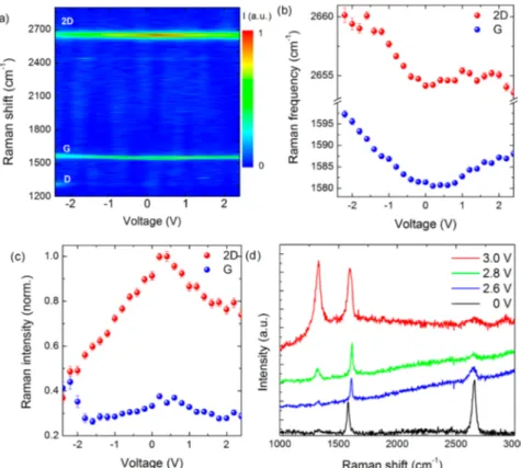
The parallel plate geometry allows us to measure the Raman spectra of graphene electrodes to monitor the electrostatic doping as function of bias voltage. The two-dimensional (2D) map of Raman intensity is plotted in Figure 3a against the Raman shift and the bias voltage. We observed strong voltage dependent Raman spectra indicating strong electrostatic Figure 2.(a) Picture of the fabricated graphene supercapacitor. The black regions are carbon electrodes that are used to make electrical contact to graphene. (b) The normalized change of the transmission of the capacitor plotted against wavelength and bias voltage. (c) The variation of the normalized change of the transmission versus the wavelength for various bias voltages. (d) Fermi energy (scattered plot) extracted from the electro-optical response of the capacitor and measured capacitance (solid red curve). Both Fermi energy and the capacitance show∼(n)1/2dependence.
doping. Figure 2b,c show the voltage dependence in Raman frequency and Raman intensity of G and 2D bands, respectively, obtained from the fitting of the Raman peaks. The G-band shows a profound change in the Raman frequency; on the other hand, 2D band shows strong change in the Raman intensity. The physical mechanisms behind these behaviors are
different. The frequency change of the G-band can be
understood by tunable electron−phonon coupling.22,23 How-ever, the mechanism of the intensity change of 2D band is due to change of possible inelastic light scattering pathways at large Fermi energies.12 Furthermore, we observed a distinguished asymmetry between electron and hole doping. Electron doping (at negative bias voltages) is significantly larger than hole doping (at positive bias voltage) likely because of different g a t i n g - s t r e n g t h o f a n i o n s ( B F4− 1) a n d c a t i o n s ((CH3CH2CH2CH2)4N1+) of the electrolyte.24 The results
obtained from the Raman spectra suggest that under a bias voltage, the Fermi energy of the top and the bottom graphene electrodes are different owing to the asymmetric doping levels, therefore, we could only modulate absorption of one graphene electrode that results around 2% modulation. Raman spectra of graphene electrodes under large bias voltages (Figure 3d) shows strong defect mode (band). The appearance of D-band is irreversible indicating structural damages of graphene due to a redox reaction.
With the aqueous electrolyte, we were able to reach |2EF|
values up to 1.8 eV. This upper limit is defined by the
electrochemical window of the electrolyte. To overcome this limitation, we used a special ionic liquid (diethymethyl (2-methoxyethyl) ammonium bis (trifluoromethylsulfony) imide) with large electrochemical window (from−3.5 to +3 V). Ionic liquids have superior performance as an electrolyte owing to Figure 3.(a) Intensity map of Raman scattering of the graphene electrode as a function of Raman shift and applied voltage. The labels indicate the D, G, and 2D Raman peaks of graphene. (b,c), Variation of Raman frequency and intensity of 2D and G bands as a function of bias voltage. (d) Raman spectra of defected graphene electrodes after application of bias voltages larger than the electrochemical window of the electrolyte.
Figure 4.(a) Normalized change of the transmission of a graphene supercapacitor that uses ionic liquid as an electrolyte for bias voltage in the range of−5 to 0 V. (b) The cutoff energy (2Ef) as a function of bias voltage. (c) Illustration of gate-induced change of Fermi energy for top and bottom
their large electrochemical window, higher ion concentrations, and low vapor pressures. Furthermore, the double layer capacitance of ionic liquids are larger than aqueous electrolyte due to very thin (<1 nm) Helmholtz layer.24We measured the electro-optical response of the ionic liquid-based graphene supercapacitor. The modulation of the optical transmission is plotted in Figure 4a. We were able to apply bias voltages in the range of−5 to +3.5 V which yields |2EF| values up to 2.3 eV (Figure 4b) without detrimental effects on the graphene electrodes. Interestingly, for high negative bias voltages (Vb < −3.5 V), we observed an additional shoulder of modulation at long wavelength likely due to blocking the interband transition of the second graphene electrode. For aqueous electrolyte, we usually observed modulation strength around 2% owing to the doping of only one graphene electrode. In the case of ionic liquid, we observed the same asymmetry; however, at high voltages we observed the modulation of the second electrode. The illustration of the optical modulation mechanism of the capacitor is shown in Figure 4c. The bias voltage drops unevenly at the quantum capacitance of the top and bottom graphene layers owing to the asymmetric charge doping. Maximum charge density achieved with ionic liquid electrolyte
is around 7× 10¹³ 1/cm2, which yields Fermi energy of 1.15 eV. At a certain wavelength, wefirst observe optical modulation due to the one electrode; at large bias voltages, the interband transition of the second graphene is blocked resulting in additional modulation. The measured capacitance and extracted 2|Ef| do not match exactly for the ionic liquid electrolyte. There are two reasons that could cause this deviation. Thefirst one is the high level of unintentional doping. From the transport measurement of the supercapacitor structure with ionic liquid electrolyte, we observed that the Dirac point is shifted to +1 and−1 V (Supporting Information, Figures S6 and S7). This shift is larger than the aqueous electrolyte likely due to the unintentional doping of ionic liquid that induces more residue charges on graphene. The second one is the low interfacial capacitance of the double layer of ionic liquid. Even the ionic density is very high for the ionic liquid, the mobility of ions are much slower than the aqueous electrolyte. Therefore, the measured capacitance (at 20 Hz) underestimates the actual capacitance of the device.
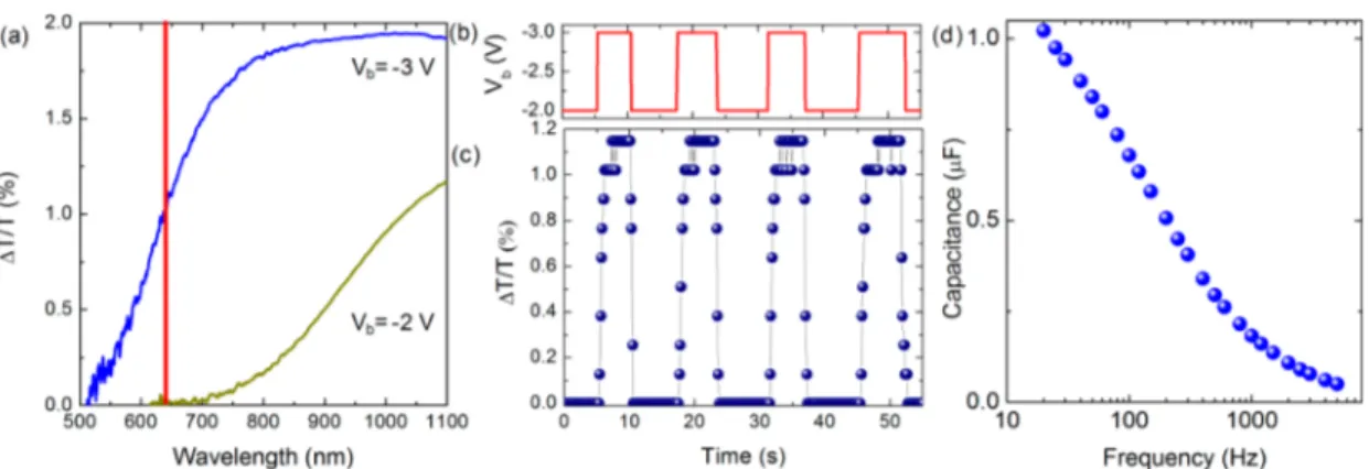
Ionic liquid electrolyte allows us to shift the optical modulation down to visible spectra. We studied the switching performance of the modulator at the wavelength of 635 nm Figure 5.(a) Normalized transmission of the capacitor at bias voltages of−2 and −3 V. The vertical red line indicated the working wavelength (635 nm). (b) Time trace of the bias voltage applied between graphene electrodes. (c) Time trace of the normalized transmission. (d) The variation of the total capacitance as a function of frequency at a bias voltage of 0 V.
Figure 6.Graphene supercapacitors using (a) single layer and (b) multilayer graphene electrodes. (c) Reflection type graphene optical modulator. (d) Normalized transmission of the graphene supercapacitor with multilayer graphene electrodes. (e) Normalized reflection of the graphene supercapacitor with a reflecting surface.
total capacitance (Figure 5d). The differential capacitance at high frequencies decays significantly due to the low ionic conductivity of the ionic liquid.
Optical absorption of a single layer graphene limits the modulation efficiency around 2% (Figure 6a). We proposed device strategies to increase the modulation efficiencies by increasing the interaction of light with graphene electrodes. Figure 6 provides the illustration of the supercapacitor
structures to increased modulation strength. In the first
approach (Figure 6b), we increase the number of graphene layers. We grew multilayer graphene (∼7−10 layers, Support-ing Information, Figure S8−S10) on copper foils and transferred them on glass substrates. Figure 6d shows the measured normalized transmittance of the capacitor with multilayer graphene electrodes. We obtained a modulation around 10%. Unlike single layer graphene electrode, multilayer graphene yield more abrupt changes at large bias voltages. Furthermore, we tested the multilayer graphene electrodes formed by layer-by-layer transfer-printing process. However, we do not obtain significant increase in the modulation strength (around 2−4%) mainly because of air gap or organic residues that remain between the graphene layers that prevent efficient gating of underneath graphene layers. For CVD grown multilayer graphene, however, layers stack by van der Walls forces, therefore, the underneath graphene layers can be gated by thefield of the ionic liquid electrolyte. Note that due to the low density of states of graphene top graphene layer cannot
completely screen the penetration of electric field of the
electrolyte.25 We observed that ionic liquid electrolyte can block the optical transition of graphene up to 5−7 layers. In the second design, we used a reflecting surface (the external side of the substrates is coated with 100 nm Ag) to double the interaction of light with graphene electrode. With this reflection type device geometry, light passes through the graphene layers two times. We measured the reflectance from the sample for various bias voltages (Figure 6e). We obtained a modulation strength of around 35% in the near-infrared and around 20% modulation in the visible. The modulation strength can be further increase by multiple reflections or by placing the super capacitor in an optical cavity.
As a conclusion, we report optical modulators operating over
a broad range of wavelengths from 450 nm to 2μm based on
graphene supercapacitors. The demonstrated device has simple parallel-plate geometry, and shows a very efficient device operation. We also studied various device geometries to increase the modulation amplitude. We were able to obtain 35% modulation using a few layer graphene with an ionic liquid electrolyte. Another advantage of the supercapacitor structure is the symmetry of the device with respect to the polarization of light. Since the supercapacitor structure has parallel plate geometry, it can provide polarization independent modulation,
optical devices ranging from plasmonics to optoelectronics. Furthermore, graphene supercapacitor can be fabricated on flexible substrates (Supporting Information, Figure S13) that can be used as electrically reconfigurable flexible coatings or smart windows. The supercapacitor structure with ionic liquid electrolyte (they have very low vapor pressures) is also compatible with ultrahigh vacuum systems that could enable optical measurements at cryogenic temperatures to reveal the fundamental properties of graphene.
■
ASSOCIATED CONTENT*
S Supporting InformationAdditional information and figures. This material is available free of charge via the Internet at http://pubs.acs.org.
■
AUTHOR INFORMATIONCorresponding Author
*E-mail: [email protected]. Phone: +90 3122908078.
Notes
The authors declare no competingfinancial interests.
■
ACKNOWLEDGMENTSThis work was supported by the Scientific and Technological Research Council of Turkey (TUBITAK) Grants 110T304, 109T209, and 112T686 and Marie Curie International Reintegration Grant (IRG) Grant 256458, Turkish Academy of Science (TUBA-Gebip).
■
REFERENCES(1) Li, Z. Q.; Henriksen, E. A.; Jiang, Z.; Hao, Z.; Martin, M. C.; Kim, P.; Stormer, H. L.; Basov, D. N.Nat. Phys. 2008, 4 (7), 532−535.
(2) Wang, F.; Zhang, Y. B.; Tian, C. S.; Girit, C.; Zettl, A.; Crommie, M.; Shen, Y. R.Science 2008, 320 (5873), 206−209.
(3) Xia, F. N.; Avouris, P.IEEE Photonics J. 2011, 3, 293−295. (4) Mak, K. F.; Ju, L.; Wang, F.; Heinz, T. F.Solid State Commun. 2012,152 (15), 1341−1349.
(5) Sensale-Rodriguez, B.; Yan, R. S.; Kelly, M. M.; Fang, T.; Tahy, K.; Hwang, W. S.; Jena, D.; Liu, L.; Xing, H. G.Nat. Commun. 2012, 3, 780.
(6) Min, H.; MacDonald, A. H.Phys. Rev. Lett. 2009, 103, 067402. (7) Horng, J.; Chen, C. F.; Geng, B. S.; Girit, C.; Zhang, Y. B.; Hao, Z.; Bechtel, H. A.; Martin, M.; Zettl, A.; Crommie, M. F.; Shen, Y. R.; Wang, F.Phys. Rev. B 2011, 83 (16), 165113.
(8) Vicarelli, L.; Vitiello, M. S.; Coquillat, D.; Lombardo, A.; Ferrari, A. C.; Knap, W.; Polini, M.; Pellegrini, V.; Tredicucci, A.Nat. Mater. 2012,11 (10), 865−871.
(9) Lee, S. H.; Choi, M.; Kim, T. T.; Lee, S.; Liu, M.; Yin, X.; Choi, H. K.; Lee, S. S.; Choi, C. G.; Choi, S. Y.; Zhang, X.; Min, B.Nat. Mater. 2012, 11 (11), 936−941.
(10) Kim, J.; Son, H.; Cho, D. J.; Geng, B. S.; Regan, W.; Shi, S. F.; Kim, K.; Zettl, A.; Shen, Y. R.; Wang, F.Nano Lett. 2012, 12 (11), 5598−5602.
(11) Ju, L.; Geng, B. S.; Horng, J.; Girit, C.; Martin, M.; Hao, Z.; Bechtel, H. A.; Liang, X. G.; Zettl, A.; Shen, Y. R.; Wang, F.Nat. Nanotechnol. 2011, 6 (10), 630−634.
(12) Wang, F.; Chen, C. F.; Park, C. H.; Boudouris, B. W.; Horng, J.; Geng, B. S.; Girit, C.; Zettl, A.; Crommie, M. F.; Segalman, R. A.; Louie, S. G.Nature 2011, 471 (7340), 617−620.
(13) Zhang, X.; Liu, M.; Yin, X. B.; Ulin-Avila, E.; Geng, B. S.; Zentgraf, T.; Ju, L.; Wang, F.Nature 2011, 474 (7349), 64−67.
(14) Gan, X. T.; Shiue, R. J.; Gao, Y. D.; Mak, K. F.; Yao, X. W.; Li, L. Z.; Szep, A.; Walker, D.; Hone, J.; Heinz, T. F.; Englund, D.Nano Lett. 2013,13 (2), 691−696.
(15) Majumdar, A.; Kim, J.; Vuckovic, J.; Wang, F.Nano Lett. 2013, 13 (2), 515−518.
(16) Yoo, J. J.; Balakrishnan, K.; Huang, J. S.; Meunier, V.; Sumpter, B. G.; Srivastava, A.; Conway, M.; Reddy, A. L. M.; Yu, J.; Vajtai, R.; Ajayan, P. M.Nano Lett. 2011, 11 (4), 1423−1427.
(17) Miller, J. R.; Outlaw, R. A.; Holloway, B. C.Science 2010, 329 (5999), 1637−1639.
(18) Zhu, Y. W.; Murali, S.; Stoller, M. D.; Ganesh, K. J.; Cai, W. W.; Ferreira, P. J.; Pirkle, A.; Wallace, R. M.; Cychosz, K. A.; Thommes, M.; Su, D.; Stach, E. A.; Ruoff, R. S.Science 2011, 332 (6037), 1537− 1541.
(19) Luryi, S.Appl. Phys. Lett. 1988, 52 (6), 501−503.
(20) Xia, J. L.; Chen, F.; Li, J. H.; Tao, N. J.Nat. Nanotechnol. 2009, 4 (8), 505−509.
(21) Ponomarenko, L. A.; Yang, R.; Gorbachev, R. V.; Blake, P.; Mayorov, A. S.; Novoselov, K. S.; Katsnelson, M. I.; Geim, A. K.Phys. Rev. Lett. 2010, 105, 13.
(22) Efetov, D. K.; Kim, P.Phys. Rev. Lett. 2010, 105, 256805. (23) Yan, J.; Zhang, Y. B.; Kim, P.; Pinczuk, A.Phys. Rev. Lett. 2007, 98, 166802.
(24) Fedorov, M. V.; Kornyshev, A. A.J. Phys. Chem. B 2008, 112 (38), 11868−11872.
(25) Uesugi, E.; Goto, H.; Eguchi, R.; Fujiwara, A.; Kubozono, Y.Sci. Rep. 2013, 3, 1595.