DESIGN OF A C-BAND DUAL-POLARIZED
STRIP-FED APERTURE COUPLED
STACKED PATCH PLANAR ANTENNA
ARRAY FOR POINT-TO-POINT
COMMUNICATION
a thesis submitted to
the graduate school of engineering and science
of bilkent university
in partial fulfillment of the requirements for
the degree of
master of science
in
electrical and electronics engineering
By
Caner ASBAS
¸
August 2017
DESIGN OF A C-BAND DUAL-POLARIZED STRIP-FED APER-TURE COUPLED STACKED PATCH PLANAR ANTENNA ARRAY FOR POINT-TO-POINT COMMUNICATION
By Caner ASBAS¸ August 2017
We certify that we have read this thesis and that in our opinion it is fully adequate, in scope and in quality, as a thesis for the degree of Master of Science.
Vakur B. ERT ¨URK (Advisor)
Ergin ATALAR
Hatice ¨Ozlem AYDIN C¸ ˙IV˙I
Approved for the Graduate School of Engineering and Science:
Ezhan KARAS¸AN
ABSTRACT
DESIGN OF A C-BAND DUAL-POLARIZED
STRIP-FED APERTURE COUPLED STACKED PATCH
PLANAR ANTENNA ARRAY FOR POINT-TO-POINT
COMMUNICATION
Caner ASBAS¸
M.S. in Electrical and Electronics Engineering Advisor: Vakur B. ERT ¨URK
August 2017
Point-to-point (P2P) communication is utilized where each communication node knows the physical or electrical positions of the other. In this type of communica-tion, only two nodes transmit/receive message between each other and no other node is included in this process. P2P communication offers some advantages such as lower power consumption, better information safety, lower vulnerablity to jam-ming and better channel capacity usage. With these properties, it is preferred frequently in military.
Directional antennas with high gain and low side lobe level (SLL) are desired for P2P communication in order to achieve higher effective communication dis-tance, lower power consumption and to decrease the interference between chan-nels, respectively. Another requirement is caused by Multiple-Input-Multiple-Output capability, which is a technique to use dual or circularly polarized tran-sreceiver antennas instead of using separate transmitter and receiver antennas in the system. For dual-polarized MIMO antennas, high cross polarization isolation values are desired to separate the transmitting and receiving channels in order to prevent them effecting each other.
In this study, a C-band dual-polarized strip-fed aperture coupled stacked patch antenna array for P2P communication is designed. To satsify the requirements of P2P communication, the reflection coefficient of the designed antenna is -10dB. The gain is 20dB and SLL is better than -15dB in the cardinal and intercardinal planes of the antenna for both polarizations. Additionally, 40dB cross polariza-tion isolapolariza-tion can be achieved. The idea is based on planar array of strip-fed dual-polarized aperture coupled patch antennas with stripline feed networks. By
iv
adjusting the amplitude distribution on the feed network, -15dB SLL in both cardinal and intercardinal planes is achieved for both polarizations. In order to block the coupling between feed networks for different polarizations and prevent distortion on amplitude and phase distributions, stripline feed networks are cho-sen. In this way, cross polarization isolation can be increased as well. Hence, a novel antenna element, dual-polarized strip-fed aperture coupled stacked patch antenna is proposed. The parameters that affect the impedance behaviour of this type of antenna are investigated and examined in detail. Required feed net-works to achieve -15dB SLL in cardinal and intercardinal planes are designed. The proposed antenna elements are placed in array sturucture, connected to feed networks and the resulted antenna array is optimized and analyzed.
Keywords: Point-to-point (P2P) communication, side lobe level (SLL) reduction, aperture coupled patch antenna, strip-fed antenna.
¨
OZET
NOKTADAN NOKTAYA TELEKOM ¨
UN˙IKASYON ˙IC
¸ ˙IN
C BANT DUAL POLAR˙IZE S
¸ER˙IT BESLEME
AC
¸ IKLIK BA ˘
GLAS
¸IMLI D ¨
UZLEMSEL B˙IR
YI ˘
GINLANMIS
¸ YAMA ANTEN D˙IZ˙IS˙I TASARIMI
Caner ASBAS¸
Elektrik ve Elektronik M¨uhendisli˘gi, Y¨uksek Lisans Tez Danı¸smanı: Vakur B. ERT ¨URK
A˘gustos 2017
Noktadan noktaya telekom¨unikasyondan, her bir ileti¸sim d¨u˘g¨um¨u di˘gerinin fizik-sel ya da elektrikfizik-sel konumunu bildi˘ginde faydalanılır. Bu tip ileti¸simde, sadece iki d¨u˘g¨um birbiri arasında mesaj alır ya da g¨onderir ve ba¸ska bir d¨u˘g¨um bu s¨urece dahil edilmez. Noktadan noktaya telekom¨unikasyon; d¨u¸s¨uk g¨u¸c sarfı, geli¸smi¸s bilgi g¨uvenli˘gi, d¨u¸s¨uk karı¸stımaya a¸cıklık ve geli¸smi¸s kanal kapasite kullanımı gibi birtakım avantajlar sunar. Bu ¨ozellikleriyle noktadan noktaya telekom¨unikasyon askeri uygulamalarda sıklıkla tercih edilmektedir.
Noktadan noktaya telekom¨unikasyon i¸cin g¨orece y¨uksek etkin ileti¸sim mesafesi ile d¨u¸s¨uk g¨u¸c sarfını sa˘glamak ve kanallar arası giri¸simi d¨u¸s¨urmek amacıyla y¨uksek kazan¸clı ve d¨u¸s¨uk yan kulak seviyeli y¨onl¨u antenler tercih edilmektedir. Di˘ger bir gereksinim, sistemde ayrı ayrı g¨onderme ve alma antenleri yerine dual yada dairesel polarize alma/g¨onderme antenleri kullananmaya dayanan bir teknik olan C¸ oklu Girdi C¸ oklu C¸ ıktı (MIMO) metodundan kaynaklanmaktadır. Dual pola-rize MIMO antenleri i¸cin alma ve g¨onderme kanallarının birbirini etkilemesinin ¨
onlenmesi ve birbirinden ayrılması amacıyla y¨uksek ¸capraz polarizasyon izolas-yonu tercih edilmektedir.
Bu ¸calı¸smada, noktadan noktaya telekom¨unikasyon i¸cin C bant dual polar-ize ¸serit besleme a¸cıklık ba˘gla¸sımlı d¨uzlemsel bir yı˘gınlanmı¸s yama anten dizisi tasarlanmı¸stır. Noktadan noktaya telekom¨unikasyon gereksinimlerini kar¸sılamak amacıyla tasarlanan antenin yansıma katsayısı -10dB’dir. Anten kazancı 20dB’dir ve yan kulak seviyesi anay¨on ve aray¨on d¨uzlemlerinde her iki polarizasyon i¸cin -15dB’dir. Ayrıca 40dB ¸capraz polarizasyon izolasyona ula¸sılmı¸stır. Bu
vi
¸calı¸smadaki fikir, ¸serit besleme hat a˘gına sahip bir ¸serit beslemeli dual polar-ize a¸cıklık ba˘gla¸sımlı yama anten d¨uzlemsel dizisidir. Besleme hattı a˘gındaki genlik ve faz da˘gılımı ayarlanarak her iki polarizasyon i¸cin anay¨on ve aray¨on d¨uzlemlerinde -15dB yan kulak seviyesi sa˘glanmı¸stır. Farklı polarizasyonlar arasındaki ba˘gla¸sımı ve genlik ile faz da˘gılımındaki bozulmaları engellemek i¸cin ¸serit hat besleme a˘gı se¸cilmi¸stir. B¨oylece ¸capraz polarizayon izolasy-onu da arttırılmı¸stır. Bu sebeple, yeni bir anten elemanı, dual polarize ¸serit besleme a¸cıklık ba˘gla¸sımlı yı˘gınlanmı¸s yama anten ¨onerilmi¸stir. Bu tip antenin empedans davranı¸sını etkileyen parametreler tespit edilmi¸s ve detaylıca ince-lenmi¸stir. Anay¨on ve aray¨on d¨uzlemlerinde -15dB yan kulak seviyesini sa˘glamak i¸cin gerekli besleme a˘gı tasarlanmı¸stır. ¨Onerilen anten elemanları dizi ortamına yerle¸stirilmi¸s, besleme a˘gına ba˘glanmı¸s ve elde edilen anten dizisi optimize ve analiz edilmi¸stir.
Anahtar s¨ozc¨ukler : Noktadan noktaya telekom¨unikasyon, yan kulak seviyesi azaltımı, a¸cıklık ba˘gla¸sımlı yama anten, ¸serit beslemeli anten.
vii
Acknowledgement
I would like express my gratitude to my supervisor Prof. Vakur B. ERT ¨URK for his supervision and support throughout my studies. I would also thank Prof. Dr. Ergin ATALAR and Prof. Dr. ¨Ozlem AYDIN C¸ ˙IV˙I, the members of my jury, for accepting to read and review my thesis.
I would like to express my gratidute to Aselsan Inc. for letting me conduct my research, and giving me permission to use the facilities. I am grateful to Mehmet Erim ˙INAL, ¨Ozkan SA ˘GLAM and Kadir ˙IS¸ER˙I for their valuable comments and support. I would also like to thank Turkish Scientific and Technological Research Council - Science Fellowships and Grant Programmes Department, T ¨ UB˙ITAK-B˙IDEB, for their financial assistance in my graduate study.
I would also like to extend my graditudes to my elder sister Nilay, my mother Nuray and my father Ahmet for their encouragement and endless support.
Contents
1 Introduction 1
2 Single Element Design 8
2.1 Proposed Single Element Structure . . . 9
2.2 Final Form of the Single Antenna Element . . . 13
2.3 Parametric Tests . . . 18
2.3.1 Lower Patch Length (lP atchLower) . . . 19
2.3.2 Upper Patch Length (lP atchU pper) . . . 21
2.3.3 Lower Spacer Thickness (dSpacerLower) . . . 23
2.3.4 Upper Spacer Thickness (dSpacerU pper) . . . 25
2.3.5 Slot Length (lSlot) . . . 27
2.3.6 Minimum of Slot Width (dSlot) . . . 29
2.3.7 Maximum of Slot Width (dSlot+ wSlot) . . . 31
CONTENTS x
2.3.9 Stub Length for Upper Feed (lStubU pper) . . . 35
2.3.10 Distance between Branches of Lower Feed (wLower) . . . . 37
2.3.11 Distance between Branches of Upper Feed (wU pper) . . . . 39
2.3.12 Distance between Reflector and Lower Ground (hRef lector) . 41
3 Feed Network Design 44
3.1 Feed Network Design Steps . . . 53
3.1.1 Step 1: Dividing Power 3P to Power 2P and P . . . 55
3.1.2 Step 2: Dividing Power 6P to Power 3P, 2P and P . . . . 57
3.1.3 Step 3: Dividing Power 12P to Power P, 2P, 3P, 3P, 2P and P . . . 59
3.1.4 Step 4: Entire Feed Network . . . 61
4 Antenna Array Design 74
List of Figures
2.1 Exploded view of the proposed single antenna element . . . 9
2.2 Side view of the proposed single antenna element . . . 10
2.3 Lower (a) and upper (b) patch and their parameters . . . 10
2.4 Top view of slots with their parameters . . . 11
2.5 Upper (a) and lower (b) feed networks with their parameters with respect to slots . . . 11
2.6 Simulated S-parameters of the finalized antenna element versus frequency . . . 14
2.7 The gain behavior of a typical strip-fed aperture coupled stacked patch antenna versus θ at φ =0◦ plane when upper feed is excited 14 2.8 The gain behavior of a typical strip-fed aperture coupled stacked
patch antenna versus θ at φ =45◦ plane when upper feed is excited 15 2.9 The gain behavior of a typical strip-fed aperture coupled stacked
patch antenna versus θ at φ =90◦ plane when upper feed is excited 15 2.10 The gain behavior of a typical strip-fed aperture coupled stacked
LIST OF FIGURES xii
2.11 The gain behavior of a typical strip-fed aperture coupled stacked patch antenna versus θ at φ =0◦ plane when lower feed is excited 16 2.12 The gain behavior of a typical strip-fed aperture coupled stacked
patch antenna versus θ at φ =45◦ plane when lower feed is excited 17 2.13 The gain behavior of a typical strip-fed aperture coupled stacked
patch antenna versus θ at φ =90◦ plane when lower feed is excited 17 2.14 The gain behavior of a typical strip-fed aperture coupled stacked
patch antenna versus θ at φ =135◦ plane when lower feed is excited 18 2.15 Reflection coefficient for upper feed network versus frequency for
various lower patch lengths . . . 19
2.16 Reflection coefficient for lower feed network versus frequency for various lower patch lengths . . . 20
2.17 Coupling between upper and lower feed networks versus frequency for various lower patch lengths . . . 20
2.18 Reflection coefficient for upper feed network versus frequency for various upper patch lengths . . . 21
2.19 Reflection coefficient for lower feed network versus frequencies for various upper patch lengths . . . 22
2.20 Coupling between upper and lower feed networks versus frequencies for various upper patch lengths . . . 22
2.21 Reflection coefficient for upper feed network versus frequency for various lower spacer heights . . . 23
2.22 Reflection coefficient for lower feed network versus frequency for various lower spacer heights . . . 24
LIST OF FIGURES xiii
2.23 Coupling between upper and lower feed networks versus frequency for various lower spacer heights . . . 24
2.24 Reflection coefficient for upper feed network versus frequency for various upper spacer heights . . . 26
2.25 Reflection coefficient for lower feed network versus frequency for various upper spacer heights . . . 26
2.26 Coupling between upper and lower feed networks versus frequency for various upper spacer heights . . . 27
2.27 Reflection coefficient for upper feed network versus frequency for various slot lengths . . . 28
2.28 Reflection coefficient for lower feed network versus frequency for various slot lengths . . . 28
2.29 Coupling between upper and lower feed networks versus frequency for various slot lengths . . . 29
2.30 Reflection coefficient for upper feed network versus frequency for various values of minimum of slot widths . . . 30
2.31 Reflection coefficient for lower feed network versus frequency for various values of minimum of slot widths . . . 30
2.32 Coupling between upper and lower feed networks versus frequency for various values of minimum of slot widths . . . 31
2.33 Reflection coefficient for upper feed network versus frequency for various values of maximum of slot widths . . . 32
2.34 Reflection coefficient for lower feed network versus frequency for various values of maximum of slot widths . . . 32
LIST OF FIGURES xiv
2.35 Coupling between upper and lower feed networks versus frequency for various values of maximum of slot widths . . . 33
2.36 Reflection coefficient for upper feed network versus frequency for various lengths of stubs of lower feed . . . 34
2.37 Reflection coefficient for lower feed network versus frequency for various lengths of stubs of lower feed . . . 34
2.38 Coupling between upper and lower feed networks versus frequency for various lengths of stubs of lower feed . . . 35
2.39 Reflection coefficient for upper feed network versus frequency for various lengths of stubs of upper feed . . . 36
2.40 Reflection coefficient for lower feed network versus frequency for various lengths of stubs of upper feed . . . 36
2.41 Coupling between upper and lower feed networks versus frequency for various lengths of stubs of upper feed . . . 37
2.42 Reflection coefficient for upper feed network versus frequency for various distances between branches of lower feed . . . 38
2.43 Reflection coefficient for lower feed network versus frequency for various distances between branches of lower feed . . . 38
2.44 Coupling between upper and lower feed networks versus frequency for various distances between branches of lower feed . . . 39
2.45 Reflection coefficient for upper feed network versus frequency for various distances between branches of upper feed . . . 40
2.46 Reflection coefficient for lower feed network versus frequency for various distances between branches of upper feed . . . 40
LIST OF FIGURES xv
2.47 Coupling between upper and lower feed network versus frequency for various distances between branches of upper feed . . . 41
2.48 Reflection coefficient for upper feed network verus frequency for various distances between reflector and the lowest ground plane . 42
2.49 Reflection coefficient for lower feed network verus frequency for various distances between reflector and the lowest ground plane . 42
2.50 Coupling between upper and lower feed networks verus frequency for various distances between reflector and the lowest ground plane 43
3.1 Desired array factor at φ =0◦ (a cardinal plane) for various fre-quencies . . . 46
3.2 Desired array factor at φ =45◦ (an intercardinal plane) for various frequencies . . . 47
3.3 Desired array factor at φ =90◦ (a cardinal plane) for various fre-quencies . . . 47
3.4 Desired array factor at φ =135◦(an intercardinal plane) for various frequencies . . . 48
3.5 Expected antenna array gain pattern at φ =0◦ (a cardinal plane) for various frequencies for the upper feed network . . . 49
3.6 Expected antenna array gain pattern at φ =45◦ (an intercardinal plane) for various frequencies for the upper feed network . . . 49
3.7 Expected antenna array gain pattern at φ =90◦ (a cardinal plane) for various frequencies for the upper feed network . . . 50
3.8 Expected antenna array gain pattern at φ =135◦ (an intercardinal plane) for various frequencies for the upper feed network . . . 50
LIST OF FIGURES xvi
3.9 Expected antenna array gain pattern at φ =0◦ (a cardinal plane) for various frequencies for the lower feed network . . . 51
3.10 Expected antenna array gain pattern at φ =45◦ (an intercardinal plane) for various frequencies for the lower feed network . . . 51
3.11 Expected antenna array gain pattern at φ =90◦ (a cardinal plane) for various frequencies for the lower feed network . . . 52
3.12 Expected antenna array gain pattern at φ =135◦ (an intercardinal plane) for various frequencies for the lower feed network . . . 52
3.13 Entire feed network (both for upper and lower feed network) . . . 54
3.14 Geometry of the feed network Section#1 . . . 55
3.15 Power distribution for the feed network Section#1 through the desired frequency band . . . 56
3.16 Phase differences for the feed network Section#1 through the de-sired frequency band . . . 56
3.17 Geometry of the feed network Section#2 . . . 57
3.18 Power distribution for the feed network Section#2 through the desired frequency band . . . 58
3.19 Phase differences for the feed network Section#2 through the de-sired frequency band . . . 58
3.20 Geometry of the feed network Section#3 . . . 59
3.21 Power distribution for the feed network Section#3 through the desired frequency band . . . 60
LIST OF FIGURES xvii
3.22 Phase differences for the feed network Section#3 through the de-sired frequency band . . . 60
3.23 The final configuration of the entire feed network . . . 61
3.24 Amplitude distribution of the entire feed network through the de-sired frequency band . . . 62
3.25 Phase distribution of the entire feed network through the desired frequency band . . . 63
3.26 Numerically obtained array factors at φ =0◦ for various frequencies 66 3.27 Numerically obtained array factors at φ =45◦ for various frequencies 67 3.28 Numerically obtained array factors at φ =90◦ for various frequencies 67 3.29 Numerically obtained array factors at φ =135◦ for various frequencies 68 3.30 Expected antenna array pattern at φ =0◦ for the upper feed
net-work for various frequencies . . . 69
3.31 Expected antenna array pattern at φ =45◦ for the upper feed net-work for various frequencies . . . 69
3.32 Expected antenna array pattern at φ =90◦ for the upper feed net-work for various frequencies . . . 70
3.33 Expected antenna array pattern at φ =135◦ for the upper feed network for various frequencies . . . 70
3.34 Expected antenna array pattern at φ =0◦for the lower feed network for various frequencies . . . 71
3.35 Expected antenna array pattern at φ =45◦ for the lower feed net-work for various frequencies . . . 71
LIST OF FIGURES xviii
3.36 Expected antenna array pattern at φ =90◦ for the lower feed net-work for various frequencies . . . 72
3.37 Expected antenna array pattern at φ =135◦ for the lower feed network for various frequencies . . . 72
4.1 Exploded view of the proposed antenna array configuration . . . . 75
4.2 S-parameters of the entire antenna array versus frequency over the desired band . . . 76
4.3 The entire array gain pattern at φ =0◦ for upper feed network for various frequencies . . . 77
4.4 The entire array gain pattern at φ =45◦ for upper feed network for various frequencies . . . 77
4.5 The entire array gain pattern at φ =90◦ for upper feed network for various frequencies . . . 78
4.6 The entire array gain pattern at φ =135◦ for upper feed network for various frequencies . . . 78
4.7 The entire array gain pattern at φ =0◦ for lower feed network for various frequencies . . . 79
4.8 The entire array gain pattern at φ =45◦ for lower feed network for various frequencies . . . 79
4.9 The entire array gain pattern at φ =90◦ for lower feed network for various frequencies . . . 80
4.10 The entire array gain pattern at φ =135◦ for lower feed network for various frequencies . . . 80
LIST OF FIGURES xix
4.11 Reflection coefficients of each single element versus frequency in the antenna array for the upper feed network . . . 82
4.12 Reflection coefficients of each single element versus frequency in the antenna array for the lower feed network . . . 82
4.13 Cross polarization isolation of each single element versus frequency in the antenna array . . . 83
4.14 Array patterns without the feed network at φ =0◦ for the upper feed network for various frequencies . . . 83
4.15 Array patterns without the feed network at φ =45◦ for the upper feed network for various frequencies . . . 84
4.16 Array patterns without the feed network at φ =90◦ for the upper feed network for various frequencies . . . 84
4.17 Array patterns without the feed network at φ =135◦ for the upper feed network for various frequencies . . . 85
4.18 Array patterns without the feed network at φ =0◦ for the lower feed network for various frequencies . . . 85
4.19 Array patterns without the feed network at φ =45◦ for the lower feed network for various frequencies . . . 86
4.20 Array patterns without the feed network at φ =90◦ for the lower feed network for various frequencies . . . 86
4.21 Array patterns without the feed network at φ =135◦ for the lower feed network for various frequencies . . . 87
4.22 Reflection coefficients of each single element versus frequency in the antenna array for the upper feed network in the presence of the grid . . . 90
LIST OF FIGURES xx
4.23 Reflection coefficients of each single element versus frequency in the antenna array for the lower feed network in the presence of the grid . . . 91
4.24 Cross polarization isolation of each single element versus frequency in the antenna array in the presence of the grid . . . 91
4.25 Array pattern in the presence of the grid without the feed network at φ =0◦ for the upper feed network for various frequencies . . . 92 4.26 Array pattern in the presence of the grid without the feed network
at φ =45◦ for the upper feed network for various frequencies . . . 92 4.27 Array pattern in the presence of the grid without the feed network
at φ =90◦ for the upper feed network for various frequencies . . . 93 4.28 Array pattern in the presence of the grid without the feed network
at φ =135◦ for the upper feed network for various frequencies . . 93 4.29 Array pattern in the presence of the grid without the feed network
at φ =0◦ for the lower feed network for various frequencies . . . . 94 4.30 Array pattern in the presence of the grid without the feed network
at φ =45◦ for the lower feed network for various frequencies . . . 94 4.31 Array pattern in the presence of the grid without the feed network
at φ =90◦ for the lower feed network for various frequencies . . . 95 4.32 Array pattern in the presence of the grid without the feed network
at φ =135◦ for the lower feed network for various frequencies . . 95 4.33 Exploded view of the proposed antenna array configuration in the
presence of the grid structure . . . 98
4.34 S-parameters of the entire antenna array in the presence of the grid versus frequency over the desired band . . . 99
LIST OF FIGURES xxi
4.35 The entire array gain pattern at φ =0◦ for the upper feed network in the presence of the grid for various frequencies . . . 100
4.36 The entire array gain pattern at φ =45◦ for the upper feed network in the presence of the grid for various frequencies . . . 100
4.37 The entire array gain pattern at φ =90◦ for the upper feed network in the presence of the grid for various frequencies . . . 101
4.38 The entire array gain pattern at φ =135◦for the upper feed network in the presence of the grid for various frequencies . . . 101
4.39 The entire array gain pattern at φ =0◦ for the lower feed network in the presence of the grid for various frequencies . . . 102
4.40 The entire array gain pattern at φ =45◦ for the upper feed network in the presence of the grid for various frequencies . . . 102
4.41 The entire array gain pattern at φ =90◦ for the upper feed network in the presence of the grid for various frequencies . . . 103
4.42 The entire array gain pattern at φ =135◦for the upper feed network in the presence of the grid for various frequencies . . . 103
List of Tables
2.1 Antenna design parameters with nominal values . . . 13
3.1 Amplitude distribution for antenna array . . . 45
3.2 Desired and numerically obtained (via HFSS) power distributions for the feed network . . . 64
3.3 Desired and numerically obtained (via HFSS) phase distributions for the feed network . . . 65
4.1 Minimum inter-element isolation of antenna elements for the upper feed network . . . 88
4.2 Minimum inter-element isolation of antenna elements for the lower feed network . . . 89
4.3 Minimum inter-element isolation of antenna elements for the upper feed network in the presence of the grid . . . 96
4.4 Minimum inter-element isolation of antenna elements for the lower feed network in the presence of the grid . . . 97
Chapter 1
Introduction
Point-to-point (P2P) communication is utilized where each communication node knows the physical or electrical positions of the other. A telephone call or a telegraph message can be regarded as simple examples for P2P communication. In P2P communication, only two communicated nodes transmit/receive message between each other and no other node is included in this process. In this aspect, P2P communication is in contrast to point-to-multipoint (P2MP) communication or broadcasting where one node transmits messages to many nodes at the same time [1].
Although digital communication by electromagnetic waves seems a recent de-velopment in terms of communication, it dates back to ancient times. The first recorded P2P communication was performed during Trojan War by King Agamemnon using torches and signal fires to send messages to his wife [2]. How-ever, modern P2P communication was started in 1816 in France. This system was based on transmitting electric sparks via wires and constituted an initial point for modern telegraphs. Over the years, wired systems have been substituted with wireless systems. In 1896, the first point-to-point wireless communication link was established [3]. Nowadays, wireless link communication has a significant role in P2P communication.
P2P communication has various advantages over P2MP communication. First of all, since the position of the node to be communicated is known, all the avail-able power can be tried to be delivered to this node. In this way, the power consumption can be decreased with respect to P2MP communication or broad-casting that transmits the available power to all communication nodes [4]. This situation also results in higher effective communication distance. Interference is another point that should be considered. With P2P communication, links are allocated to determined communications and lower interference in these links can be reached compared to P2MP communication [5]. Also, limitation with only two communication nodes provides the system with information safety since it is not preferred to deliver signals through the directions where the communicated node is not located. Lower vulnerability to jamming can be regarded as another advantage of P2P communication [6]. With wireless P2P, it is desired to get signals from the direction of the node to be communicated, and received signals from other directions are kept under a limit value. In this way, jamming vulnera-bility is decreased. Because of the aforementioned features, P2P communication is preferred frequently in military.
On the other hand, P2P communication has some disadvantages. The only available propagation mode for P2P communication is line-of-sight (LoS) propa-gation. Other mechanisms such as skywave or ground wave propagations cannot be benefitted in this type of communication. This fact limits us with two different conditions. The first one is about available frequencies for P2P communication. Low frequencies such as middle frequency (MF) and high frequency (HF), where ground wave and skywave propagations are dominant, cannot be used for P2P communication. On the other hand, due to higher frequencies such as Ka- or Ku-band, signals become more vulnerable to free path loss and this limits the ef-fective distance for P2P communication. Therefore, middle frequency bands such as C-band and E-band are frequently prefered in order to provide higher effective communication depending on the application. Secondly, due to LoS propagation, it is required to ensure that line of sight should not include obstacles and sources of fade.
for the antennas used for P2P communication. Firstly, since the position of the node to be communicated is known, antennas should be directional. Otherwise, all the available power cannot be transmitted only to the node, but it is trans-mitted through some other directions as well. In addition to that, bidirectional antennas cannot be used as the information safety cannot be ensured because undesired nodes can receive signals from other directions. Another requirement is caused by the interference effect. In order to decrease the interference between communications performed in separate links, the side lobe level (SLL) should be kept under an acceptable level. Moreover, SLL is also important in terms of jamming. When the SLL is high, the node becomes vulnerable to be jammed in the directions where the node to be communicated is not located. As it is mentioned, low frequency bands such as HF are not proper for P2P communi-cation. On the other hand, higher frequency bands suffer more from path loss. That means middle frequencies such as E-band or C-band are more appropriate for P2P communication.
Another desired requirement in P2P communication is Multiple-Input Multiple-Output (MIMO) capability. MIMO is a technique used to multiply the channel link capacity by using transmitting and receiving antennas at both the source (transmitter) and the destination (receiver) at the same time [7]. In order to achieve such MIMO capability, one can use dual or circularly polarized tran-sreceiver antennas instead of using separate transmitter and receiver antennas in a system. Hence, the physical space is reduced, which is another desired feature. However, note that dual-polarized antennas require high cross polarization iso-lation to separate the transmitting and receiving channels. Otherwise, channels obtain signals from each other and the quality of communication decreases. On the other hand, when circularly polarized antennas are used, axial ratio (a param-eter that indicates the difference between orthogonal components of the antenna gain) becomes important. A higher axial ratio value (which is undesired) means antenna gain cannot be divided equally or closely into the components and we receive/transmit less signal power via one polarization. This fact yields again a low communication quality. The choice whether circular or dual linear polariza-tion must be used is usually determined by the requirements of the radio of the
communication system.
In the literature, there are various types of antennas used for P2P commu-nication. Reflector antennas are one of the types of antennas for this purpose. They have high gain, low SLL and high cross polarization isolation. With these properties, they are useful for P2P communication. On the other hand, they are bulky structures, not low profile and not easy to install due to their paraboloid reflector components. A variety of reflector antennas is proposed for P2P commu-nication in [8]-[16]. In [8], the proposed antenna is a C-band Gregorian reflector antenna of diameter 2.4m with a reflection coefficient of -17dB and a cross po-larization isolation of 25dB. In [9], a C-band, dual-gridded reflector antenna is proposed. The anntenna in this work has 26dBi gain and 33dB cross polarization isolation. [10] presents conceptual information about C-, Ka- and Ku-band dual-gridded reflector antennas. In [11], the design of a reflector antenna in L-band with a -25dB SLL and a 29dBi gain is presented. However, the dimensions of this antenna is 8m x 2m and it is a bulky structure. [12] presents a solution for Brasilsat B3 case which provides the cities in the Amazon region with satellite communication. The antenna in this study is a dual C- and Ku-band reflector with a diameter of 2.4m. In [13], the design of a reflector antenna in S-band is presented. This antenna has -14dB reflection coefficient and 38dBi gain. The diamater for this antenna is 2.6m. In [14], a feed antenna for a reflector antenna in S-band is proposed. [15] proposes a C-band multifeed reflector antenna. More-over, [16] is another solution for Brasilsat case. The proposed antenna in [16] is a C-band reflector antenna with a 29dBi gain and a 33dB cross polariation isolation. On the other hand, horn antenna is another type of antenna preferred in P2P communication. It has similar properties with a reflector antenna. How-ever, horn antennas are not low profile and easy to install. [17]-[20] can be given as examples of studies for horn antennas that are used in P2P communication. In [17], the proposed antenna is a C/X dual-band horn antenna with a reflection coefficient lower than -16.5dB, though it additionally includes a reflector antenna that has a 2.7m diameter. In [18], a C-band horn antenna is proposed. The horn is hexagonal shaped with a reflection coefficient lower than -17dB and a cross polarization level lower than -28dBi. The proposed antenna in [19] is an L/C
band corrugated dual-slot horn. It has a reflection coefficient lower than -20dB and its cross polarization level is lower than -20dB. [20] proposes a horn antenna with a mode converter in C-band. The dimension of the antenna is 24cm x 30cm. Gain of it is higher than 19dBi and its VSWR is better than 1.5. -9dB SLL in E-plane and -20dB SLL in H-plane are achieved in [20] as well.
Antenna arrays are another option and may even be prefered in P2P commu-nication. They allow us to synthesis desired patterns by adjusting amplitude and phase distribution on the array elements. Different types of antenna elements such as Vivaldi antenna, dipole antenna or patch antenna can be used as the single element in an antenna array depending on the physical and electrical re-quirements. Among the available elements for antenna arrays, microstrip patch antennas offer some advantages. It is possible to design low profile and easy to install antenna arrays, called panel antennas, with patch antennas. [21]-[28] give examples for such panel antennas. [21] proposes an antenna whose operating frequency band is 2.5GHz - 2.7GHz. Its reflection coefficient is -10dB, it has a cross polarization level of -10dB and its gain is 8dB. Furthermore, this antenna is dual-polarized, that means it is capable of MIMO. In [22], the design of another dual-polarized antenna for P2P communication is presented. It works at 5.5GHz. It is a 4x4 planar array and 40dB cross polariation isolation is achieved in this work. In [23], a planar dual-polarized antenna similar to previous studies is pre-sented. However, the operating frequency is 2.6GHz. The proposed array in [24] is a 6x6 planar antenna array with a Wilkinson power divider as its feed network. It is composed of circularly polarized antennas that are dual-fed square stacked patch antennas and the axial ratio is better than 1.5dB. The operating frequency is reported as 1.9GHz - 2.6GHz band. 7dB gain, -21 dB reflection coefficient (better than 1.2 VSWR) and 23dB cross polarization isolation are achived in this band. In [25], 40dB gain is achieved with a -15dB reflection coefficient (better than 1.5 VSWR) by using 16x32 elements. The dimensions of the antenna array is 80cm x 42cm. [26] proposes an antenna array which consists of patches fed by dogbone slots. The feeding is nonuniform to perform beam shaping. The array is single polarized and a -30dB reflection coefficient (better than 1.1 VSWR) can be reached. [27] proposes a dual-polarized and dual-band (X- and S-band) antenna
array which consists of patch and ring-resonant antennas. The S-band antenna is a 2x1 ring-resonant antenna array with a 9.5dB gain, -22dB reflection coefficient (better than 1.2 VSWR), 25dB cross polarization isolation and -10dB SLL. The X-band antenna is a 4x8 circular patch series fed antenna array with a 18dB gain, -19dB reflection coefficient, 30dB cross polarization isolation. In [28], the proposed antenna is a dual-polarized aperture coupled patch 2x2 antenna array with a -13dB reflection coefficient. Moreover, its cross polarization isolation is 22dB and SLL is -13dB. In the literature, other antenna arrays which constist of other types of antenna elements than patch antennas can be found for P2P communication. In [29], an array of grid elements with -10dB reflection coeffi-cient, 17dB gain and -12dB SLL between 77GHz and 85GHz is proposed. Horn antennas are also used as array elements. For instance in [30], the design of 6x24 horn antenna array at Ku-band is presented. Rectangular waveguides in [31] and monopulse antennas in [32] are other antenna elements used for arrays in P2P communication. On the other hand, proper antenna elements for array struc-ture in P2P communication are still being studied in the literastruc-ture. In [33], a microstrip fed microstrip triband antenna is proposed. This antenna operates at 1.8GHz, 2.4GHz and 3.5GHz for wireless communication applications. Its gain is 2dB. In [34], the antenna is a dual-polarized slot coupled stacked patch antenna. It is fed by H-shaped slots and its cross polariation isolation is 36dB.
The aim of this thesis is to propose a C-band strip-fed dual-polarized aperture coupled stacked patch antenna array for P2P communication. The operation band is chosen as 4.4GHz to 5GHz. In order to satisfy the requirements for P2P communication, the minimum gain is aimed to be 20dB and the desired cross po-larization isolation is 40dB. Additionally, SLL is desired to be at least is -15dB for both cardinal and intercardinal planes unlike similar works where SLL is limited to 15dB only in cardinal planes. Note that cardinal planes can be defined as the cuts for φ=0◦ and φ=90◦ when antenna is placed on the xy-plane as the direction of antenna placement is x- and y-directions [35]. The intercardinal planes are the cuts except cardinal planes, i.e, planes for φ=45◦ and φ=135◦. Moreover 10◦ 3dB beamwidth is aimed. The proposed antenna is a planar array of strip-fed dual-polarized aperture-coupled patch antenna that has stripline feed networks
with required amplitude and phase distribution. By adjusting the amplitude dis-tributions, -15dB SLL in both cardinal and intercardinal planes can be reached for both polarizations. By considering the beamwidth and gain requirements, the approximate size of the antenna array should be 5.8λ, and hence we can satisfy these requirements via 6 by 6 antennas with an interelement spacing of 0.96λ. This structure provides us with conformal and easy to install geometry. How-ever, a dual-polarized aperture coupled stacked patch antenna with stripline feed does not exist in literature although there are some works on single polarized ones as in [36]. The main contribution of this thesis is the design of a strip-fed dual-polarized aperture coupled stacked patch antenna. In this way, the feed net-works for different polarizations can be separated with ground planes and proper amplitude and phase distribution to constitute the desired array factor can be achieved. If microstrip feed network and microstrip fed aperture coupled patch antenna were chosen for the array, the amplitude and phase distributions of feed networks for different polarizations would be distorted due to coupling between them when they are stacked, and the resulted array factor would not satisfy the requirements of P2P communication. Briefly, this work includes three steps that are to design the feed network with the desired amplitude and phase distributions, to design the single antenna element that is compatible with the structure of the feed network, and to make antenna elements and feed network operate together properly in array environment.
In Chapter 2, structure of the proposed single antenna element is presented. Also, the parameters that affect the behavior of the single antenna element are in-vestigated. The final design of the single element is also provided in this chapter. In Chapter 3, firstly the required amplitude and phase distributions are deter-mined. Then, the feed network that realizes the desired distribution is designed systematically. In Chapter 4, the single elements are placed in the array configu-ration and the feed network is connected, thereby finalizing the design process of the antenna array. Finally, conclusions and future work are presented in Chapter 5.
Chapter 2
Single Element Design
Aperture coupled patch antennas were first proposed by Pozar in [37]. These antennas consist of two substrates; one of them contains radiating element, and the other one includes the feed network. Over the years, dual-polarized aperture coupled patch antennas have been presented as discussed in [38] and [39]. These antennas are based on microstrip technology. Due to the feed network used, dual-polarized aperture coupled patch antennas with stripline technology are required for this work. However, available antennas in the literature are single polarized. Therefore, in this thesis, we propose a novel antenna type which is dual-polarized strip-fed aperture coupled stacked patch antenna.
The simulations in this chapter are performed via HFSS R in a computer having
32GB RAM and 2.8GHz Intel R i7 microprocessor. In the simulation model, all
metallic surfaces (patches, ground planes etc.) are modelled as copper. The antenna element is fed by waveports. A vacuum box in the shape of rectangular parallelpiped is defined around the antenna element. The minimum distance from the single antenna element to the vacuum box is λ/4 for the minimum frequency in the solution band. The solution frequency is chosen as the maximum frequency in the solution band. For the adaptive solution, maximum number of passes is determined as 15 and maximum of Delta S is determined as 0.02.
2.1
Proposed Single Element Structure
The details of the proposed antenna structure are depicted from Fig. 2.1 to Fig. 2.5.
Figure 2.2: Side view of the proposed single antenna element
Figure 2.4: Top view of slots with their parameters
Figure 2.5: Upper (a) and lower (b) feed networks with their parameters with respect to slots
This structure can be regarded as a modified dual-polarized aperture coupled patch antenna. The first modification is about the ground planes. Since stripline based feed network is used, the single element is also changed to a stripline structure. However, in order to operate the slots properly, it is observed that all the ground planes should have identical slots as a result of simulations due to the symmetry requirement. These slots are designed in the form of dog-bone shaped. In this way, dilatation of the slot width becomes an extra parameter to tune the antenna to meet the desired specifications. The other modification is the reflector plane at the bottom of the configuration as shown in Fig. 2.2. This plane reflects the radiation at the back to the front. Also note that, stacked patches are used to obtain two different resonance frequencies. On the other hand, it is not easy to operate both patches and slots at the same time. At the frequency where patches start to operate and operating of slots is ceasing, a sharp change in the impedance behavior of the antenna element is observed. In order to eliminate the change in impedance and provide smoother impedance variation, all ground planes are shorted to each other by using vias. In this way, parallel plate waveguide modes can be supressed. The cross polarization isolation is another issue that should be handled in the design of the single element. Since stripline feed is used, high cross polarization isolation can be achieved. However, to keep it higher than 40dB it is required to reshape the feeds. Instead of using a single part stripline, the 50Ω stripline feed is divided into two 100Ω stripline branches. In this way, higher cross polarization isolation (40dB) can be achieved.
For each element, foam Rohacell R51 HF material is used as the spacer and the
supporting foam. This material is a foam with low weight, low relative permit-tivity (which is 1.065) and has low tangent loss (lower than 0.0008) [40]. Since the feeding striplines are long in the feed network in order to divide the input power to 36 antenna elements, use of a substrate with high loss would result in lower antenna efficiency and lower gain. Therefore, the substrates are chosen as ROGERS 5880 Duroid Rdielectric card. It is chosen because it is a low loss card
2.2
Final Form of the Single Antenna Element
Every parameter in the proposed antenna structure causes a trade-off between reflection coefficients of upper and lower feed and cross polarization isolation. Therefore, they should be optimized with respect to the desired parameters (40dB cross polarization isolation and -10dB reflection coefficient) in the operation band (4.4GHz to 5GHz). As a result of systematic simulations, the values tabulated in Table 2.1 are chosen.
Parameter Name Value(mm) Value(λ0)
lP atchLower 20 0.313 dSpacerLower 3.5 0.055 lSlot 15.5 0.243 dSlot 3 0.047 lStubU pper 1.6 0.025 wU pper 8 0.125 hRef lector 16 0.251 wSlot 2.5 0.039 wLower 6 0.094 lStubLower 1.5 0.025 lP atchU pper 15 0.392 dSpacerU pper 2 0.031 wF eedU pper 1.4 0.022 wF eedLower 1.4 0.022
Table 2.1: Antenna design parameters with nominal values
Note that the characteristic impedance of the upper feed is tuned to 60Ω whereas it is tuned to 40Ω for the lower feed. Consequently, S-parameters and gain pat-terns for the cardinal and intercardinal planes as a result of the simulations are obtained as shown in Fig. 2.6 to Fig. 2.14. The simulations are performed from 4GHz to 5.5GHz with an increment of of 25MHz altohugh the operation band is 4.4GHz to 5GHz in order to observe the impedance characteristics of the antenna element widely.
Figure 2.6: Simulated S-parameters of the finalized antenna element versus fre-quency
Figure 2.7: The gain behavior of a typical strip-fed aperture coupled stacked patch antenna versus θ at φ =0◦ plane when upper feed is excited
Figure 2.8: The gain behavior of a typical strip-fed aperture coupled stacked patch antenna versus θ at φ =45◦ plane when upper feed is excited
Figure 2.9: The gain behavior of a typical strip-fed aperture coupled stacked patch antenna versus θ at φ =90◦ plane when upper feed is excited
Figure 2.10: The gain behavior of a typical strip-fed aperture coupled stacked patch antenna versus θ at φ =135◦ plane when upper feed is excited
Figure 2.11: The gain behavior of a typical strip-fed aperture coupled stacked patch antenna versus θ at φ =0◦ plane when lower feed is excited
Figure 2.12: The gain behavior of a typical strip-fed aperture coupled stacked patch antenna versus θ at φ =45◦ plane when lower feed is excited
Figure 2.13: The gain behavior of a typical strip-fed aperture coupled stacked patch antenna versus θ at φ =90◦ plane when lower feed is excited
Figure 2.14: The gain behavior of a typical strip-fed aperture coupled stacked patch antenna versus θ at φ =135◦ plane when lower feed is excited
It can be seen from Fig. 2.6 that the reflection coefficients are lower than -10dB for both feed networks and the cross polarization isolation (i.e., S21) is higher
than 40dB. Moreover, desired patterns for both polarizations on the cardinal and intercardinal planes are obtained as seen in Fig. 2.7 to Fig. 2.14. Therefore, the initial design of a single antenna element (i.e., strip-fed aperture coupled stacked patch antenna) is completed. In the following subsections, parametric tests on critical parameters are performed to observe their full effects on the design.
2.3
Parametric Tests
In this section, the results of parametric tests for important variables are pre-sented. In all these tests, all the parameters other than the parameter of interest are kept constant and equated to values in Table 2.1.
2.3.1
Lower Patch Length (l
P atchLower)
Since similar patterns and impedance characteristics for both polarizations are desired, the lower patch shown in Fig. 2.3(b) is designed as square. In Fig. 2.15, Fig. 2.16 and Fig. 2.17, the effect of lower patch length on the impedance characteristics is presented.
Figure 2.15: Reflection coefficient for upper feed network versus frequency for various lower patch lengths
Figure 2.16: Reflection coefficient for lower feed network versus frequency for various lower patch lengths
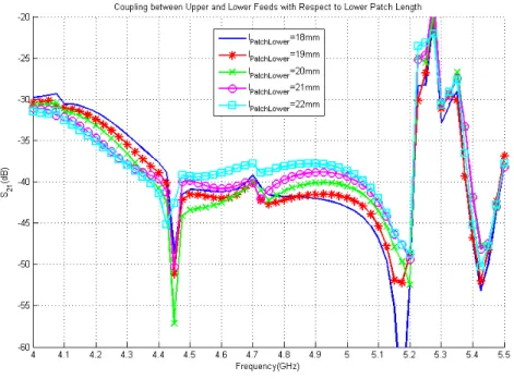
Figure 2.17: Coupling between upper and lower feed networks versus frequency for various lower patch lengths
For both lower and upper feed networks, it can be observed that an increase in the lower patch length shifts the resonance to lower frequencies. Also note that for higher values of lower patch length, the coupling between the ports increases and lower length is required for higher cross polarization isolation. It can be seen that when lP atchLower = 20mm, reflections coefficient of both upper and
lower feed networks are better than -12.5dB and the cross polarization isolation is better than 40dB. Therefore, this value is chosen.
2.3.2
Upper Patch Length (l
P atchU pper)
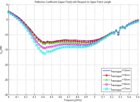
Since similar patterns and impedance characteristics for both polarizations are designed, the upper patch shown in Fig. 2.3(a) is designed as square. In Fig. 2.18, Fig. 2.19 and Fig. 2.20, the effect of upper patch length on the impedance characteristics is presented.
Figure 2.18: Reflection coefficient for upper feed network versus frequency for various upper patch lengths
Figure 2.19: Reflection coefficient for lower feed network versus frequencies for various upper patch lengths
Figure 2.20: Coupling between upper and lower feed networks versus frequencies for various upper patch lengths
It can be seen from the figures that for the upper feed network, an increase in the upper patch length decreases the magnitude of the reflection coefficient. On the other hand, for the lower feed network, an increase in this parameter shifts the resonance to lower frequencies. That means, while choosing this parameter, we are limited by the lower feed. Also note that, lower length for upper patch values cause worse cross polarization isolation. It can be seen that when lP atchU pper =
15mm, reflection coefficients of both upper and lower feed networks are better than -12.5dB and the cross polarization isolation is better than 40dB. Therefore, this value is chosen.
2.3.3
Lower Spacer Thickness (d
SpacerLower)
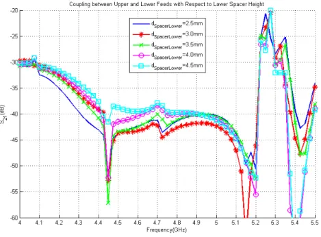
Lower spacer is placed between the upper ground plane and substrate of the lower patch as shown in Fig. 2.2. In Fig. 2.21, Fig. 2.22 and Fig. 2.23, the effect of the lower spacer thickness on the impedance characteristics is presented.
Figure 2.21: Reflection coefficient for upper feed network versus frequency for various lower spacer heights
Figure 2.22: Reflection coefficient for lower feed network versus frequency for various lower spacer heights
Figure 2.23: Coupling between upper and lower feed networks versus frequency for various lower spacer heights
It can be seen from the figures that for the upper feed network, an increase in lower spacer thickness decreases the magnitude of the reflection coefficient. On the other hand, for the lower feed network, an increase in this parameter shifts the resonance to lower frequencies. That means, while choosing this parameter, we are limited by the lower feed network. Also note that, higher lower spacer thickness values cause worse cross polarizations isolation. So, there is a trade-off between reflection coefficients and cross polarization isolation. It can be seen that when dSpacerLower = 3.5mm, reflection coefficients of both upper and lower
feed network are better than -12.5dB and the cross polarization isolation is better than 40dB. Therefore, this value is chosen.
2.3.4
Upper Spacer Thickness (d
SpacerU pper)
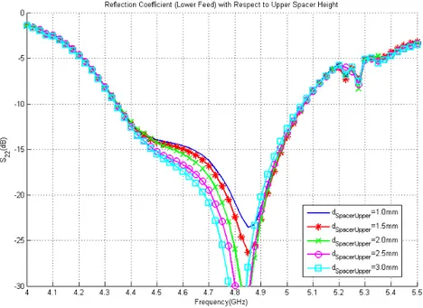
Upper spacer is placed between the lower substrate of the patch and upper sub-strate of patch as spacer as shown in Fig. 2.2. In Fig. 2.24, Fig. 2.25 and Fig. 2.26, the effect of the upper spacer thickness on the impedance characteristics is presented.
Figure 2.24: Reflection coefficient for upper feed network versus frequency for various upper spacer heights
Figure 2.25: Reflection coefficient for lower feed network versus frequency for various upper spacer heights
Figure 2.26: Coupling between upper and lower feed networks versus frequency for various upper spacer heights
It can be seen from the figures that for the upper feed network, an increase in the upper spacer thickness decreases the magnitude of the reflection coefficient. On the other hand, for the lower feed network, an increase in this parameter shifts the resonance to lower frequencies. That means, while choosing this parameter, we are limited by the lower feed network. Also note that, lower spacer thickness values cause worse cross polarization isolation. Hence, there is a trade-off between reflection coefficients and the cross polarization isolation. It can be seen that when dSpacerU pper = 2.0mm, reflection coefficients of both upper and lower feed network
are better than -12.5dB and the cross polarization isolation is better than 40dB. Therefore, this value is chosen.
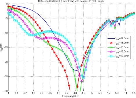
2.3.5
Slot Length (l
Slot)
In Fig. 2.27, Fig. 2.28 and Fig. 2.29, the effect of slot length, illustrated in Fig. 2.4 on the impedance characteristics is presented.
Figure 2.27: Reflection coefficient for upper feed network versus frequency for various slot lengths
Figure 2.28: Reflection coefficient for lower feed network versus frequency for various slot lengths
Figure 2.29: Coupling between upper and lower feed networks versus frequency for various slot lengths
As it can be seen from the figures, slot length does not change the reflection coef-ficient of the upper feed network significantly for the values we sweep. However, reflection coefficient of the lower feed network does change significantly, and an increase in the slot length shifts the resonance of it to higher frequencies. Also, one can observe that cross polarization isolation does not have a linear relation with the slot length and it should be optimized. Hence, there is a trade-off be-tween reflection coefficients and the cross polarization isolation. It can be seen that when lSlot = 15.5mm, the reflection coefficients of both upper and lower feed
network are better than -12.5dB and the cross polarization isolation is better than 40dB. Therefore, this value is chosen.
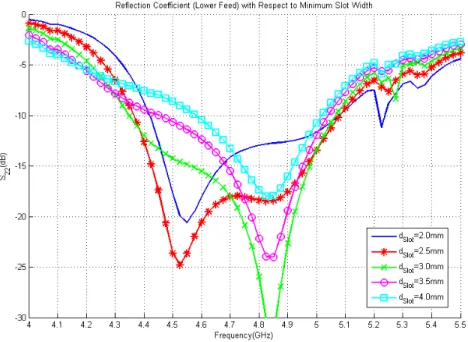
2.3.6
Minimum of Slot Width (d
Slot)
In the antenna element design, dog-bone shaped slot is chosen as shown in Fig. 2.4 due to its large bandwidth characteristics. In Fig. 2.30, Fig. 2.31 and Fig. 2.32, the effect of minimum of slot thickness, shown in Fig. 2.4, on the impedance characteristics is presented.
Figure 2.30: Reflection coefficient for upper feed network versus frequency for various values of minimum of slot widths
Figure 2.31: Reflection coefficient for lower feed network versus frequency for various values of minimum of slot widths
Figure 2.32: Coupling between upper and lower feed networks versus frequency for various values of minimum of slot widths
The results indicate that an increase in the minimum of slot width leads to shift in resonance to higher frequencies for both upper and lower feed networks. However, level of resonance changes significantly with this increase. An increase in minimum of slot width causes a dramatic decrease in the cross polarization isolation. So, there is a trade-off between resonance frequencies of the upper and lower feed networks and the cross polarization isolation. It can be seen that when dSlot = 3.0mm, reflection coefficients of both upper and lower feed networks
are better than -12.5dB and the cross polarization isolation is better than 40dB. Therefore, this value is chosen.
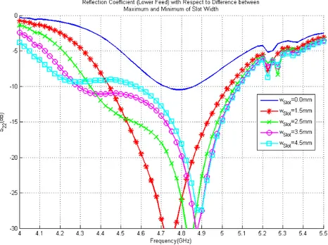
2.3.7
Maximum of Slot Width (d
Slot+ w
Slot)
In Fig. 2.33, Fig. 2.34 and Fig. 2.35, the effect of maximum of slot thickness, shown in Fig. 2.4, on the impedance characteristics is presented.
Figure 2.33: Reflection coefficient for upper feed network versus frequency for various values of maximum of slot widths
Figure 2.34: Reflection coefficient for lower feed network versus frequency for various values of maximum of slot widths
Figure 2.35: Coupling between upper and lower feed networks versus frequency for various values of maximum of slot widths
Based on Figs. 2.33 - 2.35, it can be said that an increase in maximum of slot width, the impedance bandwidth increases. On the other hand, the level of reflection coefficient can increase respectively. Additionally, note that increase in maximum of slot width causes a decrease in cross polarization isolation. So, there is a trade-off between resonance frequuencies of upper and lower feed networks and the cross polarization isolation. It can be seen that when wSlot = 2.5mm,
the reflection coefficient of both upper and lower feed network is better than -12.5dB and cross polarization isolation is better than 40dB. Therefore, this value is chosen.
2.3.8
Stub Length for Lower Feed (l
StubLower)
Open stubs are used in both polarizations for impedance matching as shown in Fig. 2.5 . In Fig. 2.36, Fig. 2.37 and Fig. 2.38, the effect of stub length for lower feed (see Fig. 2.5(b)) on the impedance characteristics are presented.
Figure 2.36: Reflection coefficient for upper feed network versus frequency for various lengths of stubs of lower feed
Figure 2.37: Reflection coefficient for lower feed network versus frequency for various lengths of stubs of lower feed
Figure 2.38: Coupling between upper and lower feed networks versus frequency for various lengths of stubs of lower feed
From these figures, one can see that an increase in the length of the open stub of the lower feed changes both the resonance frequency and the reflection level for the lower feed network. However, it has almost no effect on the upper feed network as it is expected. Another point is that, length of the open stub of the lower feed is inversely proportional to the coupling between upper and lower feed networks. Hence, there is a trade-off between the resonance frequencies of the lower feed and the cross polarization isolation. It can be seen that when lStubLower= 1.5mm,
the reflection coefficients of both upper and lower feed network are better than -12.5dB and the cross polarization isolation is better than 40dB. Therefore, this value is chosen.
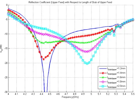
2.3.9
Stub Length for Upper Feed (l
StubU pper)
In Fig. 2.39, Fig. 2.40 and Fig. 2.41, the effect of stub length for upper feed (see Fig. 2.5(a)) on the impedance characteristics is presented.
Figure 2.39: Reflection coefficient for upper feed network versus frequency for various lengths of stubs of upper feed
Figure 2.40: Reflection coefficient for lower feed network versus frequency for various lengths of stubs of upper feed
Figure 2.41: Coupling between upper and lower feed networks versus frequency for various lengths of stubs of upper feed
Based on Figs. 2.39 - 2.41, it can be said that an increase in the length of the open stub of the upper feed changes both the resonance frequency and the reflection level for the upper feed. However, it has almost no effect on the lower feed network as it is expected. Another point is that, length of the open stub of the upper feed is inversely proportional to the coupling between the upper and lower feed networks. Hence, there is a trade-off between resonance frequencies of the upper feed and the cross polarization isolation. It can be seen that when lStubU pper = 1.6mm, reflection coefficients of both upper and lower feed network
are better than -12.5dB and the cross polarization isolation is better than 40dB. Therefore, this value is chosen.
2.3.10
Distance between Branches of Lower Feed (w
Lower)
In Fig. 2.42, Fig. 2.43 and Fig. 2.44, the effect of the distance between branches of the lower feed network, illustrated in Fig. 2.5(b), on the impedance characteristics are presented.
Figure 2.42: Reflection coefficient for upper feed network versus frequency for various distances between branches of lower feed
Figure 2.43: Reflection coefficient for lower feed network versus frequency for various distances between branches of lower feed
Figure 2.44: Coupling between upper and lower feed networks versus frequency for various distances between branches of lower feed
It can be observed from Figs. 2.42 - 2.44 that the distance between branches of the lower feed network has almost no effect on the reflection coefficient of the upper feed network. On the other hand, the resonance of the lower feed network is shifted to lower frequencies with an increase in this parameter. Additionally, a decrease in this parameter leads to a dramatic decrease in the cross polarization isolation. Hence, there is a trade-off between resonance frequencies of the lower feed and the cross polarization isolation. It can be seen that when wLower =
6.0mm, reflection coefficients of both upper and lower feed network are better than -12.5dB and the cross polarization isolation is better than 40dB. Therefore, this value is chosen.
2.3.11
Distance between Branches of Upper Feed (w
U pper)
In Fig. 2.45, Fig. 2.46 and Fig. 2.47, the effect of the distance between branches of the upper feed network, illustrated in Figs. 2.5(a), on the impedance charac-teristics are presented.
Figure 2.45: Reflection coefficient for upper feed network versus frequency for various distances between branches of upper feed
Figure 2.46: Reflection coefficient for lower feed network versus frequency for various distances between branches of upper feed
Figure 2.47: Coupling between upper and lower feed network versus frequency for various distances between branches of upper feed
It can be seen from the figures that the distance between the branches of the upper feed network has almost no effect on the reflection coefficient of the lower feed network. On the other hand, the resonance of the upper feed is shifted to lower frequencies with an increase in this parameter. Additionally, a decrease in this parameter leads to a dramatic decrease in the cross polarization isolation. Hence, there is a trade-off between resonance frequencies of the upper feed and the cross polarization isolation. It can be seen that when wU pper = 8.0mm, reflection
coefficients of both upper and lower feed networks are better than -12.5dB and the cross polarization isolation is better than 40dB. Therefore, this value is chosen.
2.3.12
Distance between Reflector and Lower Ground
(h
Ref lector)
In Fig. 2.48, Fig. 2.49 and Fig. 2.50, the effect of the distance between the reflector and the lower ground plane as illustrated in Fig. 2.1 and Fig. 2.2, on the impedance characteristics is presented.
Figure 2.48: Reflection coefficient for upper feed network verus frequency for various distances between reflector and the lowest ground plane
Figure 2.49: Reflection coefficient for lower feed network verus frequency for various distances between reflector and the lowest ground plane
Figure 2.50: Coupling between upper and lower feed networks verus frequency for various distances between reflector and the lowest ground plane
From these figures (2.48 - 2.50), the distance between the lowest ground plane and the reflector is not very effective on the impedance behavior of the upper feed network. On the other hand, it can be observed that the level of reflection coefficient of the lower feed network changes with this parameter slightly. More-over, the relation between cross polariztion isolation and this parameter is not linear. Therefore, it should be optimized. It can be seen that when hRef lector
= 16mm, reflection coefficients of both upper and lower feed network are better than -12.5dB and the cross polarization isolation is better than 40dB. Therefore, this value is chosen.
Chapter 3
Feed Network Design
In this thesis, it is aimed to design an antenna array with a -15dB SLL in both cardinal and intercardinal planes. Recall that cardinal planes are the cuts for φ=0◦ and φ=90◦ when antenna elements are placed in the x- and y-directions and intercardinal planes are the cuts for other φ’s [35]. Low SLL is desired in these planes because it results a lower interference between communication link channels and better communication quality. Additionally, vulnerability to jamming through these planes can be prevented. It is well known that the antenna pattern is the Fourier Transform of the current distribution on the antenna array. Therefore, by exciting the array elements with required amplitude and phase values, the desired array patterns can be obtained. The general practice is to feed array elements with equal amplitudes. However, this technique results in a sinc−shaped pattern and approximately -13dB SLL. Another possible amplitude distribution is the triangular amplitude distribution. That results a sinc2−shaped
pattern and -15dB SLL. Since we have a two-dimensional array, the proposed amplitude distribution should be a triangular-shaped one in both cardinal and intercardinal planes to decrease the SLL in those planes. This distribution can be called as pyramidial shape. Additionally, we require minimum 20dB gain and maximum 10◦ 3dB beamwidth. As a result, a 6 by 6 array with 0.96λ element spacing at 4.7GHz is chosen as the array configuration. Note that at 5GHz, this element spacing corresponds to 1.02λ and for high frequencies of the
band of the design, it causes grating lobes. However, in order to satisfy the gain and beamwidth requirements, this configuration is used and grating lobes are treated separetely. The angular positions for grating lobes are adjusted to angular positions of the single element pattern where directivity is 15dB lower than the maximum of the directivity at that point. In this way, the grating lobes can be supressed. The desired distribution is tabulated in Table 3.1, where P stands for unit power.
Antenna#1 Antenna#2 Antenna#3 Antenna#4 Antenna#5 Antenna#6
P 2P 3P 3P 2P P
Antenna#7 Antenna#8 Antenna#9 Antenna#10 Antenna#11 Antenna#12
2P 4P 6P 6P 4P 2P
Antenna#13 Antenna#14 Antenna#15 Antenna#16 Antenna#17 Antenna#18
3P 6P 9P 9P 6P 3P
Antenna#19 Antenna#20 Antenna#21 Antenna#22 Antenna#23 Antenna#24
3P 6P 9P 9P 6P 3P
Antenna#25 Antenna#26 Antenna#27 Antenna#28 Antenna#29 Antenna#30
2P 4P 6P 6P 4P 2P
Antenna#31 Antenna#32 Antenna#33 Antenna#34 Antenna#35 Antenna#36
P 2P 3P 3P 2P P
Table 3.1: Amplitude distribution for antenna array
Note that the desired amplitude distribution for the feed network is the matrix product of P*[1 2 3 3 2 1]T and [1 2 3 3 2 1]. Hence, the division [1 2 3 3 2 1]
should be implemented to input power at first. In this way, rows of the matrix can be obtained. Then, division [1 2 3 3 2 1] should be implemented to outputs of the first power divider separately. As a result, the matrix product can be realized. This means only one power divider [1 2 3 3 2 1] should be designed at first. Then, by combining seven of them, where one is directly connected to input power and six of them are connected between the outputs of the first divider and antenna ports, the entire feed network can be constructed. .
In the thesis, no electrical scanning is aimed and the maximum radiation is desired at boresight. Therefore, all antenna elements should be equiphase. Moreover, desired patterns are the same for both polarizations. Thus, only one 1-to-36 power divider is designed and two of them are stacked to constitute the dual-polarized feed network.
The desired amplitude and phase distributions are simulated via MATLAB Rand
ideal (i.e., desired) array factors are computed. The resulted array factors are pre-sented from 4.4GHz to 5GHz with an increment of 0.1GHz in Fig. 3.1, Fig. 3.2, Fig. 3.3 and Fig. 3.4 for cardinal and intercardinal planes. Note that the up-per and lower feed networks are the same to generate similar patterns for both polarizations. Therefore, expected (ideal) array factors are the same for them.
Figure 3.2: Desired array factor at φ =45◦ (an intercardinal plane) for various frequencies
Figure 3.3: Desired array factor at φ =90◦ (a cardinal plane) for various frequen-cies