Figure 1. TEM image of the synthesized 2-nm Si-NPs.
Abstract— In this work, the effect of embedding Silicon Nanoparticles (Si-NPs) in ZnO based charge trapping memory devices is studied. Si-NPs are fabricated by laser ablation of a silicon wafer in deionized water followed by sonication and filtration. The active layer of the memory was deposited by Atomic Layer Deposition (ALD) and spin coating technique was used to deliver the Si-NPs across the sample. The nanoparticles provided a good retention of charges (>10 years) in the memory cells and allowed for a large threshold voltage (Vt) shift (3.4 V)
at reduced programming voltages (1 V). The addition of ZnO to the charge trapping media enhanced the electric field across the tunnel oxide and allowed for larger memory window at lower operating voltages.
I. INTRODUCTION
Recently, Silicon Nanoparticles (Si-NPs) have been considered as promising candidates for charge storage elements in future high density and low power charge trapping memory devices. However, the majority of recent experimental works studied Silicon-Oxide-Nitride-Oxide-Silicon (SONOS) memory devices with ≥ 5-nm Si-NPs which exhibit bulk-like trapping characteristics [1-2]. Technologically feasible and competitive future devices require nanoparticles of sub 3-nm dimensions; a zero-dimensional regime where important modifications to the silicon electronic structure occur. Additionally, ZnO based memories have recently attracted attention due to the excellent ZnO properties which allows for promising memory devices [3-8]. In this work, laser ablated Si target was used to fabricate non-agglomerate Si-NPs which were applied in the charge storage media of ZnO-based memory devices.
II. FABRICATION
A. 2-nm Si-Nanoparticles Fabrication
Silicon nanoparticles (Si-NPs) are synthesized in a two-stage process. Initially, 100-500 nm Si-NPs are produced by
*This work is supported by the Advanced Technology Investments Company (ATIC), United Arab Emirates.
N. El-Atab, and A. Nayfeh are with the Institute Center for Microsystems – iMicro, Department of Electrical Engineering and Computer Science (EECS), Masdar Institute of Science and Technology Abu Dhabi, United Arab Emirates. (phone: +971-56-2122779; fax: +971-2-810-9101; e-mail: [email protected]).
A. Ozcan, S. Alkis and A. K. Okyay are with UNAM-Institute of Materials Science and Nanotechnology, and the Institute of Materials Science and Nanotechnology, Bilkent University, Ankara 06800, Turkey.
A. K. Okyay is with the Department of Electrical and Electronics Engineering, Bilkent University, Ankara 06800, Turkey
focusing on a Si wafer immersed in deionized water a femtosecond pulsed laser of wavelength λ = 800 nm. pulse duration of 200 fs, and an average output power of 1.6 W at a pulse repetition rate of 1 kHz. Next, Si-NPs of size ranging from 1-5.5 nm (with a dominant size of 2-nm) are synthesized by performing sonication for 200 min at 40 KHz followed by filtration of the NPs colloidal using filters with a 100-nm pore size [9]. A TEM image of the produced ultra-small Si-NPs is shown in Figure 1.
B. Memory Fabrication
The channel-last memory cells are fabricated on a highly doped (10-18 milliohm-cm) p-type (111) Si wafer. Firstly, a 360-nm-thick SiO2 layer is Plasma Enhanced Chemical Vapor Deposited (PECVD) then patterned by and etched using the Buffered Oxide Etch (BOE) for device isolation. Next, the active layers of the memory device are deposited using a Savannah 100 system Atomic Layer Deposition (ALD): first a 15-nm-thick Al2O3 blocking oxide is deposited at 250°C. Then, Si-NPs are deposited across the sample by spin coating method at a speed of 700 rpm and an acceleration of 250 rpm/sec for 10 sec. A 4-nm-thick Al2O3 tunneling oxide followed by an 11-nm-thick ZnO channel are then ALD deposited at 250°C. The ZnO channel is patterned by optical lithography and etched in a solution of 98:2 H2O:H2SO4. The source and drain contacts are created by depositing 100 nm Al using thermal evaporation followed by lift off. Finally, Rapid Thermal Annealing (RTA) at 400ºC for 10 min in forming gas (H2:N2 5:95) is performed on the devices. Similar memory devices with only Si-NPs charge storage layer (ZnO is excluded) and with 4-nm tunnel oxide are fabricated in order to study the effect of ZnO on the memory device. The fabricated memory cell structure with 2-nm Si-NPs embedded in ZnO is shown in Figure 2.
2-nm Laser-Synthesized Si Nanoparticles for Low-Power Charge
Trapping Memory Devices
Nazek El-Atab, Student Member, IEEE, Ayse Ozcan, Sabri Alkis, Ali K. Okyay, Senior Member,
IEEE, and Ammar Nayfeh, Member, IEEE
Figure 3. I-V characteristic of the memory device with Si-NPs embedded in ZnO programmed/erased at -10 V/10 V. Figure 2. Cross-section illustration of the fabricated memory device
with 2-nm Si-NPs embedded in ZnO.
Figure 5. Measured retention characteristic of the memory devices at room temperature.
Figure 4. Measured Vt shift at different programming voltages.
III. EXPERIMENTAL CHARACTERIZATION
Using the Agilent-Signatone B1505A semiconductor device analyzer, the memory devices are programmed/erased by applying -10/10 V gate voltage with the source and drain being grounded. Then, the memory state is read by sweeping the gate voltage from 0 V up 20 V with a drain voltage of 10 V and the source being grounded. The memory device is found to be programmed by applying a negative gate voltage which indicates that holes are being stored in the Si-NPs. Figure 3 shows the Idrain-Vgate of the memory with Si-NPs embedded in ZnO where a 6.3 V threshold voltage (Vt) shift is achieved. Without NPs, the measured memory window is 2.6 V while 2.9 V with Si-NPs and without ZnO. Thus the ZnO adds additional trapping states in the memory with Si-NPs embedded in ZnO. The charge trap states density of the Si-NPs can be calculated by adopting (1) in the case of the memory with only Si-NPs [10]:
Q = (Ct ×ΔVt)/(2×q) (1) where Ct is the capacitance of the charge trapping layer per unit area, ΔVt is the Vt shift, and q is the Coulomb elementary charge. The charge trap states density with a 2.9 V Vt shift is roughly 7×1012 cm-2.
The memory devices are programmed/erased at different gate voltages and the measured Vt shifts are plotted in Figure
4. The plot shows that the memory device with Si-NPs embedded in ZnO provides the largest memory windows at reduced operating voltages where a 3.4 V Vt shift is obtained at 1 V programming voltage. At this operating voltage, the electric field across the tunnel oxide is calculated using Synopsis Sentaurus Physics Based TCAD [11] and is found to be 0.36 MV/cm which is too low for tunneling mechanism to be applicable. This suggests that another emission mechanism is dominant at such low electric field.
The retention characteristic of the memory devices are also studied by first programming them at –10 V and then reading the state of the memory in time at room temperature as shown in Figure 5. The extrapolated retention of the different memory devices at 10 years shows that 41%, 57%, 100% of the initial stored charge in the memory devices with Si-NPs embedded in ZnO, Si-NPs only without ZnO, and ZnO-only is lost in 10 years, respectively. The results indicate that the retention of the memory devices can be improved and that the tunnel oxide thickness can be further reduced by adding ZnO to the charge storage media. In fact, the ZnO layer acts as an extra-layer that holes must overcome in order to leak out into the channel.
IV. ANALYSIS
Using the materials properties of ZnO, Al2O3, [12-13] and 2-nm Si-NPs, [14-17] the energy band diagram of the
Figure 7. Vt shift vs. square root of the electric field across the
tunnel oxide of the memory with Si-NPs embedded in ZnO. Figure 6. Energy band diagram of the memory with Si-NPs embedded
in ZnO charge trapping layer.
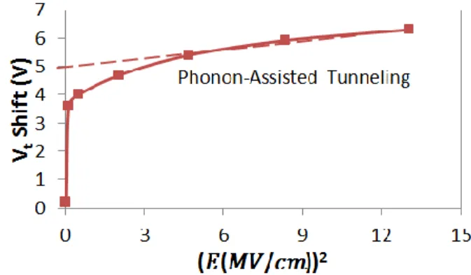
Figure 8. Vt shift vs. square of the electric field across the tunnel
oxide of the memory with Si-NPs embedded in ZnO. memory with Si-NPs embedded in ZnO is plotted in Figure
6. Component heads identify the different components of
The changes in the electronic structure of the 2 nm Si nanoparticles due to quantization and coulomb charging energy are included. In fact, it is proven that when the Si-NPs size reduces; their their dielectric constant decreases [15], bandgap increases due to quantum confinement in 0-D [17], their electron affinity decreases, and their work-function increases [16]. Additionally, the coulomb charging energy - which is defined as the energy needed to add a single electron or hole to the nanoparticle - is increased to 1.1 eV for a 2-nm Si-NP [16] where the charging energy is calculated according to (2):
Ecoul= q2/C (2) where q is the Coulomb charge and C is the capacitance of the nanoparticle given by 4πϵR, where ϵ is the dielectric constant of the nanoparticle.
Furthermore, it is shown in the plot of the energy band diagram in Figure 6 that the conduction band offset between the ZnO channel and Al2O3 tunnel oxide is larger than the valence band offset (ΔEc=1.92 eV< ΔEv=1.36 eV) which makes the holes tunneling probability exponentially greater. In addition, the conduction and valence bands of the Si-NPs are above those of the surrounding ZnO which might prevent electrons storage but allows holes storage in the Si-NPs. This analysis supports the observed holes storage in the memory device. Moreover, the large valence band offset between the Si-NPs and the tunnel oxide (ΔEv=3.09 eV) reduces the holes back-tunneling probability which exponentially enhances the retention characteristic of the memory.
However, the trapped holes in the Si-NPs in the memory without the charge trapping ZnO layer will leak out at a higher rate since the tunneling layer thickness (ZnO+Al2O3) will be reduced. The results of the retention characteristic shown in Figure 6 support this analysis.
In order to specify the hole emission mechanism in the memory devices with Si-NPs, the electric field across the tunnel oxide is calculated using Synopsys Sentaurus Physics Based TCAD` [11]. For the memory device with Si-NPs embedded in ZnO charge trapping layer, a memory window of 3.4 V is achieved at a gate voltage of 1 V which corresponds to an electric field of 0.36 MV/cm. At such low electric field, the tunneling probability is negligible. The linear trend in Figure 7 showing the measured Vt shift vs. the square root of the electric field indicates that Poole-Frenkel Effect (PFE) is the dominant emission mechanism at low electric fields E=0.36 MV/cm [18]. In fact, due to PFE, the barrier for the holes in the ZnO channel is reduced by an amount Δ which makes the holes more prone to overcoming the barrier into the tunnel oxide and then; due to the electric field, charges will be swept towards the charge storage media.
Moreover, the linear trend in Figure 8 showing the measured Vt shift vs. the square of the electric field shows that Phonon-Assisted Tunneling (PAT) is the dominant emission mechanism at higher electric fields of E > 2.7 MV/cm. In PAT, holes tunneling probability is exponentially increased due to their thermal excitation. The emission rate in PAT increases exponentially with the square of the electric field according to (3) [19-20]:
= (3) where e(E) and e(0) are the thermal ionization probabilities with and without an electric field E, respectively, and Ec is the characteristic field intensity.
In the case of the memory with only Si-NPs (without ZnO), a high programming voltage is needed in order to achieve a noticeable Vt shift as shown in Figure 4. At such high programming voltages, the electric filed across the tunnel oxide is high which suggests that tunneling mechanism is the dominant emission mechanism. In order to specify the type of the tunneling mechanism, the natural
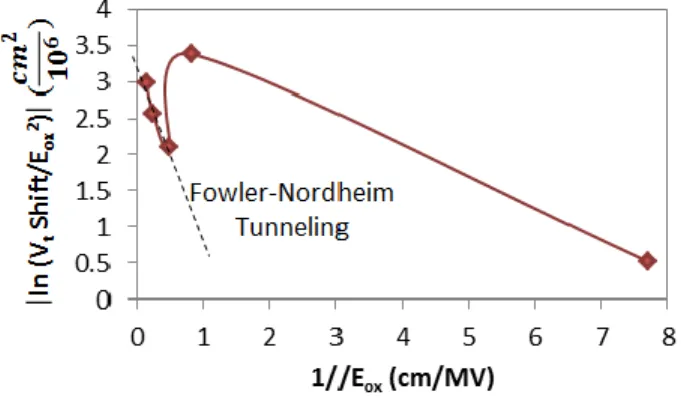
Figure 9. The natural logarithm of the Vt shift over the square of the
electric field is plotted vs. the reciprocal of the electric field. The linear trend indicates that Fowler-Nordheim is the dominant emission mechanism at an oxide electric field of 2.1 MV/cm.
across the tunnel oxide vs. the inverse of the field is plotted in Figure 9 and the linear trend at electric fields larger than 2.1 MV/cm indicate that Fowler-Nordheim (F-N) tunneling is valid. In F-N tunneling, holes tunnel through a triangular energy barrier into the tunnel oxide, and due to the high
electric field in the tunnel oxide, the holes are swept towards the Si-NPs where they get trapped. The emission rate of charges in F-N tunneling follows (4) [21]:
(4)
where J is the F-N tunneling current, C1 and C2 are constants in terms of the effective mass and barrier height and Eox is the electric field across the tunnel oxide.
Since the F-N tunneling is considered as the tunneling mechanism which requires the largest programming voltage to be applicable, therefore; the addition of the ZnO – which is n-type by nature [3] - enhances the electric field across the tunnel oxide during the program operation and allows for other emission mechanisms which operate at lower electric fields such as PFE and PAT to be applicable leading to larger memory windows at reduced operating voltages.
V. CONCLUSION
In conclusion, the effect of embedding Si-NPs in ZnO-based memory devices is demonstrated. The results show that large memory windows at reduced operating voltages with enhanced retention characteristic can be achieved by embedding the Si-NPs in a ZnO charge trapping layer. The ZnO layer adds additional trapping states, adds an additional thickness that trapped holes must overcome to leak out, and enhances the electric field across the tunnel oxide causing lower electric-field emission mechanisms to be applicable such as PFE and PAT. The results indicate that 2-nm Si-NPs embedded in ZnO are a good candidate for charge storage media in future low-cost low power nonvolatile charge trapping memory devices.
ACKNOWLEDGMENT
We gratefully acknowledge financial support for this work provided by the Advanced Technology Investment Company
(ATIC) Grant 12RAZB7. This work was supported in part by TUBITAK Grants 109E044, 112M004, 112E052 and 113M815.
REFERENCES
[1] N Nedev, D Nesheva, E Manolov, R Brüggemann, S Meier, Z Levi, and R Zlatev, “MOS structures containing silicon nanoparticles for memory device applications,” Journal of Physics: Conference Series, vol. 113, p. 012034, 2008.
[2] Lei Wang, Mei Ji, Shiwei Zhu, Hailin Tu, and Jun Du, “Synthesis and Electrical Characterization of a MOS Memory Containing Si Nanoparticles Embedded in High-k HfO2 Thin Film,” Journal of
Physics: Conference Series, vol. 152, p. 012028, 2009.
[3] N. El-Atab, S. Alqatari, F. B. Oruc, T. Souier, M. Chiesa, A. K. Okyay, and A. Nayfeh, “Diode behavior in ultra-thin low temperature ALD grown zinc-oxide on silicon, ” AIP Advances, vol. 3, p. 102119, 2013.
[4] F. B. Oruc, F. Cimen, A. Rizk, M. Ghaffari, A. Nayfeh, and A. K. Okyay, “Thin film ZnO charge-trapping memory cell grown in a single ALD step,” IEEE Elec. Dev. Lett. vol. 33, p. 1714, 2012. [5] N. El-Atab, A. Rizk, A. K. Okyay, and A. Nayfeh, “Zinc-oxide charge
trapping memory cell with ultra-thin chromium-oxide trapping layer,”
AIP Advances, vol, 3, p. 102119, 2013.
[6] Nazek El-Atab, Ayse Ozcan, Sabri Alkis, Ali K. Okyay, and Ammar Nayfeh "Low power zinc-oxide based charge trapping memory with embedded silicon nanoparticles via poole-frenkel hole emission," Appl. Phys. Lett. vol. 104, p. 013112, 2014.
[7] Nazek El-Atab, Ayse Ozcan, Sabri Alkis, Ali K. Okyay, and Ammar Nayfeh, “Silicon Nanoparticle Charge Trapping Memory Cell,” Phys. Status Solidi RRL, vol. 8, p. 629, 2014. DOI: 10.1002/pssr.201409157.
[8] Nazek El-Atab, Furkan Cimen, Sabri Alkis, Bülend Ortaç, Mustafa Alevli, Nikolaus Dietz,Ali K. Okyay, and Ammar Nayfeh, “Enhanced memory effect via quantum confinement in 16 nm InN nanoparticles embedded in ZnO charge trapping layer,” Appl. Phys. Lett. vol. 104, p. 253106, 2014.
[9] S. Alkis, A. K. Okyay, and B. Ortac, “Post-treatment of silicon nanocrystals produced by ultra-short pulsed laser ablation in liquid: toward blue luminescent nanocrystal generation,” Journal of Physical
Chemistry, vol. 116, p. 3432, 2012.
[10] C. W. Liu, C. L. Cheng, S. W. Huang, J. T. Jeng, S. H. Shiau, and B. T. Dai, “Bimetallic oxide nanoparticles CoxMoyO as charge trapping layer for nonvolatile memory device applications,” Appl. Phys. Lett., vol. 91, p. 042107, 2007.
[11] J. Bu, M. H. White, “Design considerations in scaled SONOS nonvolatile memory devices,” Solid-State Electronics, vol. 45, pp. 113-120, 2001.
[12] M. L. Huang, Y. C. Chang, C. H. Chang, T. D. Lin, J. Kwo, T. B. Wu, and M. Hong, “Energy-band parameters of atomic-layer-deposition Al2O3/InGaAs heterostructure,” Appl. Phys. Lett., 89,
012903 (2006).
[13] G. D. Wilk, R. M. Wallace, and J. M. Anthony, “High-κ gate dielectrics: Current status and materials properties considerations,” J.
Appl. Phys., vol. 89, p. 5243, 2001.
[14] J. P. Proot, C. Delerue, and G. Allan, “Electronic structure and optical properties of silicon crystallites: Application to porous silicon,” Appl.
Phys. Lett. vol. 61, p. 1948, 1992.
[15] C. Delerue and G. Allan, “Effective dielectric constant of nanostructured Si layers,” Appl. Phys. Lett.,vol. 88, p. 173117 2006. [16] D. V. Melnikov and J. R. Chelikowsky, “Electron affinities and
ionization energies in Si and Ge nanocrystals,” Physical Review B, vol. 69, p. 113305, 2004.
[17] O. M. Nayfeh, “Nonvolatile memory devices with colloidal 1.0 nm silicon nanoparticles: principle of operation, fabrication, measurements, and analysis,” Ph.D dissertation, EECS, MIT,
Cambridge, MA, 2009.
[18] W. R. Harrell, J. Frey, “Observation of Poole–Frenkel effect
saturation in SiO2 and other insulating films,” Thin Solid Films, vol.
[19] S. D. Ganichev, W. Prettl, and P. G. Huggard, “Phonon assisted tunnel ionization of deep impurities in the electric field of far-infrared radiation,” Physical Review, vol. 71, pp. 3882-3885, 1993.
[20] S. D. Ganichev, I. N. Yassievich, W. Prettl, J. Diener, B. K. Meyer, and K. W. Benz, “Tunneling ionization of autolocalized DX-centers in terahertz fields,” Phys. Rev. Lett., vol. 75, pp. 1590-1594, 1995. [21] S. M. SZE, “Nonvolatile Memory Devices,” in Physics of
Semiconductor Devices, 3rd ed. New Jersey: Wiley, 2007, ch.6, ss.7,