Physical Model for Subsurface Silicon Writing
O. Tokel1,2, A. Turnalı2, I. Pavlov1, and F. ¨O. Ilday1,2
1Department of Physics, Bilkent University, 06800 Ankara, Turkey
2Department of Electrical and Electronics Engineering, Bilkent University, Ankara, 06800, Turkey
Abstract
We have recently reported a direct laser writing method enabling buried structures deep inside sili-con. Here we study the formation of these subsur-face structures. We take advantage of Nonlinearity Engineering to understand this new phenomenon.
Summary
Micromachining of silicon (Si) with lasers is being investigated since the 1970s [1]. So far, generation of controlled subsurface modification in the bulk of Si with high precision has not been achieved. This is highly de-sirable since successful integration of Si photonics and data transfer elements with conventional Si integrated circuits is proposed to lead to new generations of micro-processors [2,3]. Available techniques fabricate these optical and electronic elements on the top layer of the silicon-on-insulator platform. Despite the remarkable successes of conventional techniques, none of the avail-able methods make use of the bulk of Si for position-ing functional elements. We have recently reported a method for photo-inducing deeply buried structures in Si wafers with pulsed infrared lasers [4].
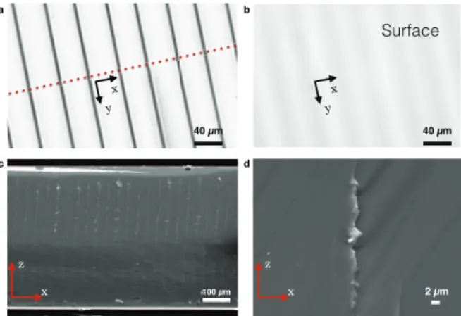
c d a x z x z Surface b 40 μm x y x y 40 μm 2 μm 100 μm
Fig. 1 Microscope images of the silicon sample after laser process-ing. The laser propagates along the z-axis in all images and processes undoped (15 kΩ.cm) Si. (a-b) Infrared transmission mode images of the wafer (a) Image acquired by focusing the objective to the centre of the silicon wafer. The plane passing through the red-dotted line and the z-axis is used in the cross-sectional SEM studies. (b) Image show-ing the surface of the wafer, indicatshow-ing that the surface is not dam-aged after subsurface processing. (c-d) Scanning electron microscope (SEM) images of the cross-section of the sample. (c) A representative view of the structures formed in the x-z plane, along the dotted line in Figure 1a. (d) A zoomed image of a single line.
A laser propagating in the z-axis is tightly focused to create subsurface structures inside silicon. Subsur-face structures manifest themselves when the micro-scope image plane is located inside the wafer surface (Fig 1a). Fig 1b shows the undamaged laser entrance
surface (xy plane) of the same sample after writing. The direct-write nature of the 3D silicon scribing allows one to create a multitude of geometries. This rich space can be used to encode information inside silicon. For in-stance we have recently demonstrated that it is possible to store information buried deep inside a silicon wafer [5]. Further we demonstrated the first functional optical element in the bulk of a silicon wafer [6].
The direct laser-writing technique allows us to rou-tinely create sub-surface nanostructures with aspect ra-tios > 300 (Fig 1c). The structures extend hundreds of micrometers along the laser propagation direction, while their widths remain on the order of a microm-eter (Fig 1d). This is particularly striking because in conventional nonlinear laser processing of transparent materials, the laser is focused to a spot and the modi-fications are quasi- one-dimensional. The observed be-haviour here is analogous to filamentation effect seen in femtosecond laser material processing in transparent media.
Filamentation is based on the Kerr nonlinearity. However our experimental power levels are an order of magnitude lower than the critical power required for the onset of this effect. Moreover, assuming the slowly varying envelope approximation with paraxial propa-gation conditions, the solution of the scalar nonlinear Schrodinger equation (NLSE) indicates that there is no self focusing effect in our experiments. It should be noted that the Rayleigh length in the experiment is 30
μm, whereas the length of the structures are at least an
order of magnitude longer than this. How can one ex-plain this effect?
To this end, we simulated the behaviour of a Gaus-sian laser beam focused inside a 500μm thick silicon wafer. The simulations were performed with the wave optics module of the Comsol package program. Comsol uses finite element methods to solve Maxwell equations. Here, we do not include any losses. We simply assume that when the intensity is above a certain threshold the material is be modified. We assume that the crystal sil-icon is modified to amorphous silsil-icon with the effect of the laser. Notably, to create these structures, the laser is not directly focused inside the sample, but behind the sample. This allows a low enough intensity not to dam-age the surface. The laser is partially reflected from the exit surface, and a nonlinear interaction ensues as de-scribed below.
The refractive index of crystal silicon is 3.47, whereas the refractive index of amorphous silicon is 3.7. This high index difference is pointing to a possible wave guiding effect during the formation of the structures. To
Fig. 2 Comsol wave optics simulations (a) Intensity profile of the beam when a 50μm amorphous silicon is induced in the focal position. (b) Intensity profile of the beam when a 100μm amorphous silicon is included in the focal position. (c) Intensity profile of the beam when a 300
μm amorphous silicon is included along the optical axis. The close-up of the wave guiding effect in shown on the right image. The consecutive
simulations are self-consistent pointing to a wave guiding effect during the formation of the structures.
test this hypothesis, we placed different length amor-phous silicon (SiA) strips along the laser propagation axis. First we use 50 μm SiA (Fig 2a), then 100 μm SiA (Fig 2b) and finally a 300μm SiA (Fig 2c). The consecutive images are self-consistent in that the newly formed structures are guiding the light and extending the length of the structures along the laser propagation axis. This shows that the formation is due to nonlinear evolu-tion with a wave guiding effect arising from the strong refractive index contrast between the two materials. By exploiting this effect, one can engineer different aspect ratio structures.
In conclusion, we report the first numerical simula-tions towards understanding sub-surface laser modifica-tion in Si. This new phenomenon is separated from the previous work in Si, in that the surface of the sample is not modified. It is shown that this effect is due to a waveguiding effect, in contrast to other transparent ma-terial processing experiments, enabling the creation of high aspect-ratio structures. We have created structure lengths ranging from 80μm to 500 μm.
The advantage of the silicon industry has always been being able to cram more complexity in the wafer. We believe this laser-writing technology will contribute to the existing silicon fabrication capabilities and will find applications in diverse fields, such as silicon
pho-tonics, optofluidics and potentially in on-chip quantum photonics experiments. Detailed understanding of sili-con laser writing is rich with nonlinear effects, and one can envisage the use of these effects in future laser-writing experiments and expand the building blocks for creating a fabrication toolbox of deep silicon engineer-ing. We also note that in this context Nonlinearity Engi-neering will take a center stage.
Acknowledgments
We acknowledge funding from The Scientific and Tech-nological Research Council of Turkey (TUBITAK) . References
[1] M. Birnbaum, “Semiconductor surface damage produced by ruby lasers,” J. Appl. Phys. 36, 3688 (1965).
[2] J. Bonse, J. Kr¨uger, S. H¨ohm and A. Rosenfeld, “Femtosecond laser-induced periodic surface structures,” J. Laser Appl. 24, 042006 (2012).
[3] B. ¨Oktem, I. Pavlov, S. llday, H. Kalaycıo˘glu, A. Rybak, S. Yavas¸, M. Erdo˘gan, and F. ¨O. llday, “Nonlinear laser lithography for indef-initely large-area nanostructuring with femtosecond pulses,” Nature Photon. 7, 897 (2013).
[4] O. Tokel, A. Turnalı, I. Pavlov, and F. ¨O. Ilday, Laser-Writing in Silicon for 3D Information Processing, arXiv:1409.2827v1 (2014) [5] O. Tokel, A. Turnalı, I. Pavlov, and F. ¨O. Ilday, Laser Writing Deep inside Silicon for 3D Information Processing, CLEO Europe, (2015). [6] A. Turnalı, O. Tokel, I. Pavlov, and F. ¨O. Ilday, Direct Laser Writ-ing of Volume Fresnel Zone Plates in Silicon, CLEO Europe, (2015).