/ W ¿і'іЛі—. .*i ■*>-> i. "* ХЛ€'іГ2!;С?Мі€Й EMG¿MEE:p¡I¿I S r^jy rp-r-f rr-:
5
:.y> ::>'г.гп^ П гргт' ^ 0^ ^'ïïI-5
’ ‘ í? г '^··.'”^' **v' ,Й|·; * ; . , ! , ' ¡ Ύ Κ 7 Í 7 / - 2 .İ3BU
A THESIS
SUBMITTED TO THE DEPARTMENT OF ELECTRICAL AND ELECTRONICS ENGINEERING
AND THE INSTITUTE OF ENGINEERING AND SCIENCES OF BILKENT UNIVERSITY
IN PARTIAL FULFILLMENT OF THE REQUIREMENTS FOR THE DEGREE OF
MASTER OF SCIENCE
By
Sanli Ergun
26 January 1994
A THESIS
SUBMITTED TO THE DEPARTMENT OF ELECTRICAL AND ELECTRONICS ENGINEERING
AND THE INSTITUTE OF ENGINEERING AND SCIENCES OF BILKENT UNIVERSITY
IN PARTIAL FULFILLMENT OF THE REQUIREMENTS FOR THE DEGREE OF
M ASTER OF SCIENCE
By
Sanli Ergun
26 January 1994
I certify that I have read this thesis and that in my opinion it is fully adequate, in scope and in quality, as a thesis for the degree of Master of Science.
Prof. Dr. Abdullah Atalar(PrincipaJ Advisor)
I certify that I have read this thesis and that in my opinion it is fully adequate, in scope and in quality, as a thesis for the degree of Master of Science.
Prof. Dr. Canan Toker
I certify that I have read this thesis and that in my opinion it is fully adequate, in scope and in quality, as a thesis for the degree of Master of Science.
UÂL
Assist. Prof. İrşadi Aksun
Approved for the Institute of Engineering and Sciences:
Prof. Dr. Mehmet Bat
Sanli Ergun
M .S. in Electrical and Electronics Engineering
Supervisor: Prof, Dr. AbduUah Atalar
26 January 1994
Using GaAs Monolithic Microwave Integrated Circuit (MMIC) technology three distributed amplifiers are realized. Two of these amplifiers employ single gate FETs and operate in the 2-18 GHz frequency range. They have 4.5 and 6.5 dB gain, respectively. The third amplifier utilizes cascode connected FETs. This amplifier operates in the 2-20 GHz range and has a gain of ~10 dB. All the three amplifiers have input and output return losses better than 10 dB. The isolation of the amplifiers with single gate FETs is better than 20 dB, whereas the cascode connection improves the isolation over 30 dB. The amplifiers are designed for a 50O-svstem. The simulations are made linearly, and the results match the theoretical work.
In the design of these amplifiers a more detailed method is used in which the artificial transmission lines are investigated and optimized in their frequency behaviour. Besides, to realize these amplifiers, a new parametrized cell library for GEC-Marconi’s F
20
foundry process is created and utilized.Keywords: MMIC, distributed amplifier, artificial transmission line, parametrized cell library
D A Ğ IT IL M IŞ Y Ü K SE LTİC İ D E V R E L E R İ
Sanlı Ergun
Elektrik ve Elektronik Mühendisliği Bölüm ü Yüksek Lisans
Tez Y öneticisi: Prof. Dr. Abdullah Atalar
26 Ocak 1994
Aynı tabana oturtulmuş (monolitik) mikrodalga tümleşik devreler uygu layımından yararlanılarak üç tane dağıtılmış yükseltici tasarlanıp üretilmiştir. Bu yükselticilerden iki tanesi tek kapılı alan etkili transistörler kullanmakta olup, 2-18 GHz düzeyinde çalışmaktadırlar. Bu yükselticilerin kazancı, sırasıyla, 5 ve 6.5 dB seviyesindedir. Üçüncü yükseltici için ardarda bağımlı alan etkili transistörlerden yararlanılmıştır. Bu yükseltici 2-20 GHz seviyesinde çalışmakta olup, yaklaşık 10 dB kazancı vardır. Bütün üç tasarımın da giriş ve çıkış yansıma yitimleri 10 d B ’den daha iyidir. Tek kapılı alan etkili transistörlerle yapılan tasarımlar 20 dB ’den daha iyi bir yalıtım sağlarken, ardarda bağımlı alan etkili transistörlerin kullanıldığı tasarımda 30 dB ’nin üstünde yalıtım elde edilmiştir. Yükselticiler 50 i î ’luk bir ortama göre tasarlanmıştır. Çözümlemeler doğrusal olarak yapılmıştır ve sonuçlar teorik çalışmalarla uyum içindedir.
Yükselticilerin tasarımında, yapay Hetişim hatlarının incelendiği ve frekansa göre davranışlarının eniyileştirildiği, daha ayrıntılı bir yöntem kullanılmıştır. Bunun yanında, yükselticileri gerçekleştirmek (yonga çizimlerinin yapılması) için, GEC-Marconi şirketinin F20 döküm işlemine dayanarak, yeni bir parametrik göze yordamlığı oluşturulmuş ve kullanılmıştır.
Anahtar kelimeler: aym tabana oturtulmuş mikrodalga tümleşik devreleri, dağıtılmış yükseltici, yapay iletişim hattı, parametrik göze yordamlığı
Rather than a list of Thanks, I will just say : Thank You,
to those special people who hold this thesis in their hands and read these lines, and feel love to me. Most special of all. Thanks to you, Alev.
1 INTRODUCTION
1
2 GaAs M ESFET and T H E IR LINEAR M O D ELIN G 3
2.1
GaAs MMIC ... 32.2
MESFET o p e ra tio n ... 52.3 Biasing and Linear modeling of M E S F E T s ... 8
2.4 Linear Design P r o c e d u r e ...
11
3 TH EOR Y OF D ISTR IB U TE D AM PLIFICATIO N 13 3.1 Constant-k Artificial Transmission L i n e s ... 13
3.2 Resistive Artificial L i n e s ... 17
3.3 Design of the Gate and Drain L in e s ... 21
3.3.1 G a t e -L in e ...
21
3.3.2 D rain-Line... 30
3.4 Gain Considerations ... 35
3.5 Design, Analysis and O p tim iz a tio n ... 52
3.6 Design A ltern atives... 63
4 TOOLS FOR TH E REALIZATION OF A M M IC D ESIG N 69 4.1 GEC-Marconi’s F20 P r o c e s s ... 69
4.2 c a d e n c e’s Layout Tool and Marconi’s element library for F
20
P rocess... 76
4.3 C O M PA C T’S simulation tool, and E X P L O R E R ... 80
5 ANALYSIS OF TH E FINAL L A Y O U T 85 5.1 L a y o u t s ... 85
5.2
Various analysis of the layout and expected measurement results 93 5.3 M easurem ents... 995.3.1 DC measurements...
100
5.3.2 RF measurements... 100
6 CON CLUSIO N 105 APPENDICES 106 A Linear Model Equations for F20 Foundry MESFETs 106 A .l F20 FET model for devices with
2
gate fin g e rs... 106A
.2
F20 FET model for devices with 4 gate fin g e rs... 110A.3 F20 FET model for devices with
6
gate fin g e rs...112
A .
4
D.C. Characterization ...114B A Pascal Program for Distributed Amplifier Design 115 B . l P r o g r a m ... 115
B.
2
Sample O u t p u t ... 123C Equivalent Models for F20 Foundry Passive Elements 126 C . l IN D U C T O R S ...126
C
.2
C A P A C I T O R S ... 131C .
2.1
Polymide C a p a c it o r s ... 131C.
2.2
Silicon Nitride C a p a c ito r ... 132C.3 RESISTORS ... 134
C.4 TRANSMISSION L IN E S ... 135
C.4.1 M3 Microstrip Transmission L in es... 135
C.4
.2
M2
Microstrip Transmission L in es... 136C.5 INTERFACE COM PONENTS ... 137
C.5.1 Bond P a d s ... 137
C.
5.2
Via H o l e s ... 138D SKILL ROUTINES FOR F20 PROCESS 139
1.1 Basic structure of a distributed a m p lifie r...
2
2.1
Typical cross-sectional structure of a MESFET ...6
2.2
Typical cross-sectional structure of a MESFET after pinch-off . 7 2.3 Typical current-voltage characteristic of a M E S F E T ...8
2.4 Linear Model of a M E S F E T ...
10
3.1 Characteristic impedance of a transmission l i n e ... 13
3.2
Infinite section artificial transmission lin e ... 143.3 Characteristic impedance of an artificial transmission line . . . . 15
3.4 Single section constant-k n e t w o r k ... 16
3.5 Short length of transmission lin e ... 18
3.6 Resistive artificial transmission line (in p u t )... 19
3.7 Resistive artificial transmission line ( o u t p u t ) ... 19
3.8 Equivalent input capacitances for
2
-fingered F E T s ... 263.9 Equivalent input capacitances for
4
-fingered F E T s ... 263.10 Equivalent input capacitances for
6
-fingered F E T s ... 273.11 Equivalent output capacitances for 2-fingered F E T s ... 31
3.12 Equivalent output capacitances for
4
-fingered F E T s ... 313.14 Simplified amplifier m o d e l ... 36
3.15 Gain with = 0Jcl<^d as parameter and Xg = 0 .4 5 ...39
3.16 Gain with Xg = udojg as parameter and x j =
2 2
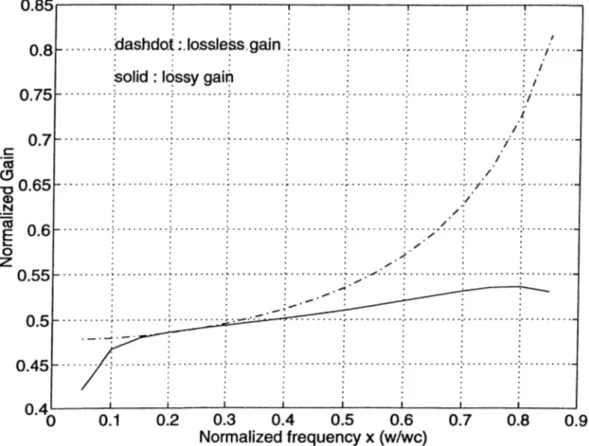
... 403.17 A comparison of the lossless gain and lossy gain; x j =
22
, Xg = 0.45, Qm = 0.0297 and = 40 . . . . ... 443.18 Gate-line attenuation, with Xg parameter... 46
3.19 Drain-line attenuation, A j, with Xd p a ra m e te r... 47
3.20 Approximation to A^, with Xg p a ram eter... 49
3.21 Approximation to A j, with Xd p a ra m eter... 49
3.22 Noj>t for Xd=22 and x ^ = 0 .4 5 ... 50
3.23 Gain for Xd=22, Xj=0.45, = 40 D and pOT=0.0297mS... 50
3.24 Return losses and isolation ... 57
3.25 No additional c a p a c ita n c e ... 58
3.26 Ca=0.2318 p F ... 58
3.27 Ca=0.13 p F ... 59
3.28 Schematic of the first d e s ig n ... 60
3.29 Optimized gain of the first d e s ig n ... 61
3.30 Schematic of the second design ... 64
3.31 Optimized gain of the second d esign ... 65
3.32 Cascode con n ection ...
66
3.33 Third d esig n ... 67
3.34 Return losses and isolation of the third d e s ig n ... 67
4.1 Geometry of a standard 4-fingered F E T ... 71
4.2 Geometry of planar and stacked spiral in d u cto rs... 72
4.3 Geometry of overlay and interdigital capacitors ... 73
4.4 Geometry of an etched resistor...
74
4.5 Geometry of a Bond Pad and a V i a ... 75
4.6 Structure of a library in C AD EN C E ... 78
4.7 S
21
of a 10 micron bend with S.Compact and EXPLORER. EX. 1:144, EX.2:484 and EX.3:1936 grid points... 824.8 A coupled line s t r u c t u r e ... 83
4.9 S
21
of a coupled line from S.Compact and E X P L O R E R ...845.1 S
21
of the first la y o u t... 875.2
S ll , s22
s l2
of the first la y o u t ...88
5.3 Minimum and the actual noise figures of the first la y o u t...
88
5.4 Gain o f the second layout ... 90
5.5
S ll , S22
and S12
of the second layout... 905.6 Minimum and the actual noise figures of the second layout . . . 91
5.7 Gain of the third layout ... 92
5.8
S ll, S22
and S12
of the third layout ... 925.9 minimum and the actual noise figures of the third layout . . . . 93
5.10 Gain of the first layout when coupled line models are used . . . 94
5.11 Gain of the second layout when coupled line models are used . . 95
5.12 Bias dependent gain variation. Id varies from 1.0 to 0.3 in 0.1 steps... 96
5.15 Gain variation with Ls p aram eter... 98
5.16 Gain variation with Rs param eter... 98
5.17 General structure of a coplanar RF p r o b e ...
100
5.18 Pad structure for RF p o r t s ... 101
5.19 Measured DC characteristics of a 2 x 98 μτη F E T ...
101
5.20 Measured S ll of the first a m p lifie r ...
102
5.21 Measured S21 of the first a m p lifie r ... 103
5.22 Measured S12 of the first a m p lifie r ... 103
5.23 Measured S22 of the first a m p lifie r ... 104
A .l Linear Model of a F20 Foundry MESFET ... 107
C .l Equivalent Model of a Planar Spiral Inductor ... 127
C.2 Resonance Frequency of Spiral Inductors w.r.t number o f turns . 127 C.3 Equivalent Model o f a Stacked Spiral In d u c to r...129
C
.4
Resonance Frequency of Spiral Inductors w.r.t prime inductance 130 C.5 Equivalent Model of an Overlay C a p a c it o r ... 132IN T R O D U C T IO N
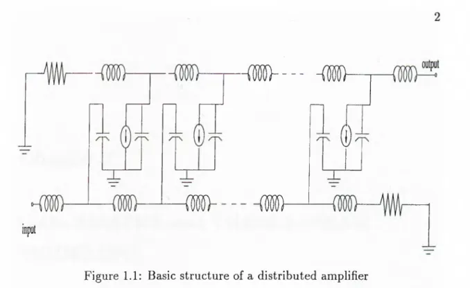
Amplifiers, in general have a gain-bandwidth constraint. Distributed am plification was first proposed by PercivaJ in 1936 as an attempt to produce an amplifier without this usual constraint [
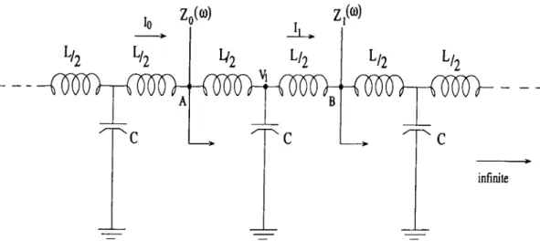
1
]. In those days electron-tubes were used as the active devices of these amplifiers. Recently, with the availability o f good-quality microwave GaAs FETs, the distributed amplifier has again become popular.When FETs are used as active devices, distributed amplification has the ca pability of adding each F E T ’s transconductance without adding their parasitic capacitances. This is accomplished by linking the parasitic input and output capacitances of the FETs by inductors to form artificial constant-k transmis sion lines. By terminating these lines b}'^ resistive loads, the unwanted signals are dissipated while the desired signals are added in-phase at the output of the amplifier. In order to have these signals added in-phase, the phase shifts of each section of the gate and drain lines must be carefully equalized. The general structure o f a distributed amplifier is shown in Fig.
1
.1
.When a signal is excited at the input terminal, a wave begins to propagate along the artificial gate line. The voltages appearing on the gate capacitance of each FET excites another wave on the artificial drain line due to the transcon ductance of each FET. This explains how the transconductances are added without adding F E T ’s parasitic capacitances. This kind of amplification is a very promising technique for very high performance amplifiers. The gate and drain lines can be designed to give 50ÎI for a very wide frequency range which means high input and output return losses. Besides, the relative insensitivity
- f i r o iW )~
(!)
iopot
Figure 1.1: Basic structure of a distributed amplifier
o f the amplifier performance to the variations of the circuit parameter, and the stable operation of these amplifiers make them very attractive. The gain and isolation properties of these amplifiers depend mostly on the device you use and are usually very good. Already 2-20 GHz decade band amplification with 30-DB gain [2], 2-18 GHz band amplification with 6.3 DB 0.5 DB gain [5], 2-18 GHz band amplification with
6
DB ^1
DB gain [6
], 2-20 GHz amplifica tion with ~24 DB gain [7], 5-60 GHz amplification with12
DB ^1
DB gain [8
] have been obtained. The amplifier topology is almost the same for all. The performance variations come from the variations in the types of devices used and the number of stages engaged.In this work, the general design method of a distributed amplifier is inves tigated, and a given class of MESFETs are analysed to see their amplification performances.
G aAs M ESFET and TH EIR L IN E A R
M O D E L IN G
2.1
G aA s M M IC
In the last
20
years Microwave Integrated Circuits(MIC) have gained exten sive popularity in many applications and have been upgraded from laboratory researches to qualified military and commercial hardware in production, due to the advancement in the development of microwave solid state devices. Fur ther, in the last decade, the concept of building a microwave “system on a chip” (pioneered in low-frequency silicon IC technology), where the effect of bond-wire parasitics can be minimized and the use of discrete elements can be avoided, is becoming real in monolithic MICs(MMIC).Microwave Integrated Circuits can be divided into two categories, namely hybrid MICs and monolithic MICs. In the h}’^brid technology, the distributed elements are fabricated, using thin or thick-film technology, on the substrate. These distributed elements are generally fabricated using single-level metalliza tion. The lumped elements are fabricated, by using multilevel deposition and plating techniques, onto the substrate or attached to it in chip form. The solid state devices are added to the substrate discretely. In the MMIC technology, all active and passive circuit elements and interconnections are formed into bulk, or onto the surface o f a semi-insulating substrate by some deposition scheme such as epitaxy, ion implantation, sputtering, evaporation, diffusion, or a combination of these processes. So, in fact, MMIC technology is a multi layer deposition process, which makes it very expensive, compared to hybrid technology. But, monolithic MICs have the capability to be fabricated in large quantities which decreases the cost per unit chip. Hybrid MICs are mostly
MICs have an obvious advantage and are preferred. This advantage is due to the fact that, circuit elements in MMICs are well-defined and in compact form. They can be made as small as the technology allows. On the other hand, this property hinders circuit tweaking and repairing, which is the most important disadvantage of MMICs against hybrid MICs. Lastly, the design flexibility and the broadband performance -due to the absence of bond wires and discrete elements- are the flashing advantages of MMICs, which give them this large popularity against hybrid MICs, especially for the last decade.
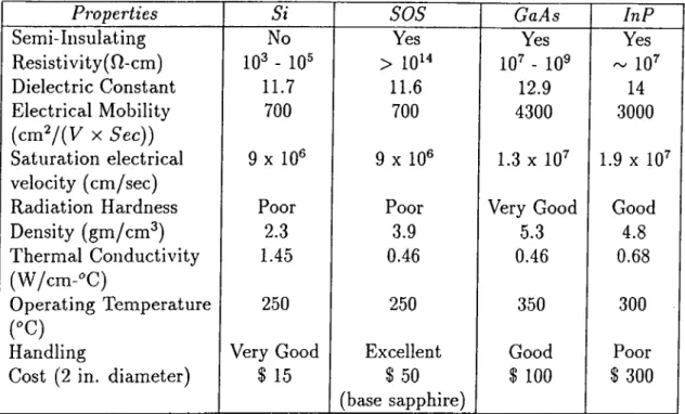
The first MMIC result was reported in 1964 [9]. It was based on silicon technology. But the results were not promising, due to the low resistivity of silicon substrate. In 1968 Mehal and Wacker [10] attempted to fabricate a 94 GHz receiver front-end using semi-insulating GaAs substrate. The results were again dissapointing due to the lack o f high-temperature technology re quired for GaAs. Since mid 1970s MMIC technology did not improve, mainly because o f the absence of an optimum processing. In 1976, Pengelly and Turner reported an X band amplifier based on GaAs MESFET [
11
]. The results were very encouraging. After that, due to the rapid development of GaAs technology and MESFETs, excellent performance of the GaAs substrate, and the fabri cated chips, many results were reported and MMIC researches have become very popular. [19]Good performance of MMICs is mostly because of the excellent performance o f GaAs as a substrate. In fact, there are several substrate materials used for MMICs. Some of them are silicon, silicon-on-sapphire(SOS), GaAs, and InP. The reason why GaAs is preferred as a substrate, can be seen when their electrical and physical characteristics are compared. [19] Table
2
.1
.Bulk Si MMIC technology is based on the bipolar transistor and is usable to S band. For SOS MMIC technology the basic active device is a silicon MESFET. The maximum operating frequency for a l//m gate-length MESFET is about
6
GHz. If GaAs is used, the maximum operating frequency of the same M ESFET is about 15 GHz. With shorter gate-length, MESFETs operating up to 100 GHz can be produced. FETs up to 60 GHz have already been reported. From these, the popularity of GaAs FETs can be explained by their higher frequency of operation and versatility. InP has the capability of operation at higher frequencies, but they had not been able to reach the performance ofElectrical Mobility (c m ^ /(y X Sec)) 700 700 4300 3000 Saturation electrical velocity (cm /sec) 9 X 10® 9 X 10® 1.3 X 10^ 1.9 X 10^
Radiation Hardness Poor Poor Very Good Good
Density (gm /cm ^) 2.3 3.9 5.3 4.8 Thermal Conductivity (W /cm -°C ) 1.45 0.46 0.46
0.68
Operating Temperature (°C) _ 250 250 350 300Handling Very Good Excellent Good Poor
Cost
(2
in. diameter) $ 15 $ 50 (base sapphire)$
100
$ 300Table
2
.1
: Comparison of some common processes with GaAsGaAs due to the low Schottky-barrier height of metals on n-type InP, and the high cost o f the InP process.
2.2
M E S F E T operation
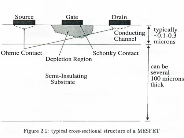
A metal-semiconductor field-effect transistor (MESFET) is a kind of JFET {junction field-effect transistor) in which the p-n junction is replaced by a Schottky junction. So a MESFET operates essentially in the same manner as a JFET. A typical cross-sectional structure of a MESFET is shown in Fig.
2
.1
.Most M ESFET devices are depletion-mode devices, which means that for zero voltage between the gate and the channel, a conductive channel exists between source and drain. Reverse biasing the Schottky diode increases the depletion region width associated with the diode, resulting in a decrease in the volume o f the channel between the drain and source. In effect, the volume of the channel, and thus the current flowing between drain and source can be modulated with the voltage applied to the gate. If the reverse bias voltage on the Schottky junction is increased, there will be a point where the depletion region covers the whole conducting channel. This voltage, where the whole channel disappears is called the pinch-off voltage, Vj>. Note that, the source
Ohmic Contact
/
Schottky Contact
Depletion Region
Semi-Insulating
Substrate
microns
can be
several
100 microns
thick
Figure
2
.1
: typical cross-sectional structure of a MESFETterminal is always at zero potential, and is a positive voltage. In other words the channel pinches off when Vga < —Vp. This potential, that causes the whole channel to be depleted, is also called the saturation field.
When the reverse-bias voltage at the gate is kept fixed and below pinch-off, and Vds is increased to a positive value, gate to channel voltage will increase on the drain side, resulting in an increase in the depletion width and a decrease in the channel width, on the drain side. This is clearly seen in Fig. 2.1.
When Vds is increased further, the channel will get narrower, and there will be a point where the depletion region on the drain side covers the whole channel, in other words, the channel on the drain side reaches the saturation field first. But, there is still a channel on the source side, as seen in Fig. 2.2. Note that, at point x, where the channel has just reached the saturation field, the channel to gate voltage must be equal to Vp. That is,
14
- Vgs = Vp, implying v ; = 14 +14-Since there is a potential difference between point x and source, and a conduct ing channel, although some portion of the channel have reached the saturation field, a current flows between drain and source terminals. Keeping Vds constant and varying Vgs, varies the depletion width and thus the volume of the existing channel. So the current still can be modulated with the signal applied to the
y . =
Vp + Vgs
S em i-In su la tin g
Substrate
D e p le t io n R e g io n
Figure
2
.2
: typical cross-sectional structure of a MESFET after pinch-off gate. Keeping Vga constant and varying Vis moves the point x between source and drain, extending or shortening the channel length. This, in effect, increases or decreases the amount of current flowing between drain and source, but this is usually a very small effect. Roughly, we can say that Vis does not effect the current flow, and the charges are injected through the depleted region of the channel. If Vgs is decreased to I^, then the all the channel will be effected by the saturation field, and as 14 will be OV in this case, there will be no current flow, whatever Vis is·Basically, the current flowing through the source and drain terminals, /¿
5
, is controlled by the gate and drain voltages. If the channel has not reached the saturation field anywhere, then the channel volume, thus its resistance, is controlled by both gate and drain voltages. That is, the channel is a voltage controlled resistor and the drain voltage is the source of current through the channel. This is called the linear operation {Vis < Vp + 14*)·*liVis ~> Vp -\· Vgsi the conducting channel is cut at the drain side, which means high impedance. There is still current flowing between the drain and source terminals which is controlled by Vgs^ as mentioned above. Vis only a slight control on this current due to the movement of point x with varying
14
,, which is usually negligible. This is called the saturation of the MESFET(I4s > Vp -f I4
j). Typical current-voltage characteristic of a MESFET can be seen in Fig. 2.3. These curves and the following approximate equations explains the'T h e linear region mentioned here has nothing to do with linearity, it is also called the non-saturation region.
h. = 20{(V„
+
V,)Vj. -
S )
Vi. <
V„
+
V,
( . )Id,=HV„+V,y{l+\Vi,)tanh(aVj,)
Vi, > VJ, + K,
(2.2)
When an enough positive voltage is applied to the gate, the Schottky diode turns on, and the junction begins to conduct. Then, a MESFET is no more a transistor.
2.3
Biasing and Linear modeling of M ESFETs
When the MESFET is biased such that it’s in non-saturation -this is accom plished by applying a Vga voltage higher than the pinch-oiF voltage and lower than the turn on voltage of the Schottky diode, and a Vj, voltage that is small enough to satisfy Vj, < Vj, + - the channel can be viewed as a nonlinear resistor. The value of this resistor is determined by the value of Vgg and Vds- If an additional AC signal is applied to the gate, with the previous discussion.
small enough.
In non-saturation, a MESFET does not make sense in amplification pur poses, as its output impedance is very low. In saturation, we have a different situation. As some part of the channel is depleted, the impedance between the drain and source terminals is very high. On the other hand, the resistance of the non-depleted channel is primarily determined by and the voltage at point X is fixed at V^-f- V^s· So, there is still a current flowing through the chan
nel, which is controlled by Vgs and is independent of Vj*. Thus, we can model the channel as a voltage controlled current source. The slight dependence of Ids on Vds can be modeled as a parallel resistance to the current source. If an additional AC signal is applied to the gate, the current Ids is modulated with the signal frequency in a non-linear fashion. This current Ids can be viewed as a DC term, IdsQ·, plus an AC term ids- If the signal level applied to the gate is small enough, then the modulation can be considered as linear, then IdsQ will be determined by the DC voltage applied to the gate, and the amplitude of ids will be determined by the amplitude of the signal applied to the gate. The linear relationship between ids and Ugs is called the small-signal transconduc tance of the MESFET, which is the re<ison for the gain. This transconductance depends on the depletion region width. If the depletion region is narrow, it is more sensitive to variations in V^j, which means a high transconductance, or vice versa. This means that the transconductance of the MESFET is also determined by
The depletion region under the gate metal is, in fact, a capacitive effect and an accumulation o f positive charges. So, the gate can be modeled as a capacitor, whose value is determined by Vgs· Also, due the finite conductance o f the gate metallisation and the contacts, there exists a small resistance in series with the capacitor. Although this resistance is small, later we will see that it is quite effective. This capacitor is labeled as Cgs and the resistance as Ri- Vgs voltage, controlling the Ids current, is, in fact, the voltage across this Cgs capacitor.
A similar capacitance, Cdg exists between drain and gate terminals, which is much smaller than Cgs due to the high reverse bias of the junction at that side. Another capacitive effect exist between drain and source terminals, mostly because of the fringing fields, Cds- Besides these, all the terminals have contact resistances and metallization inductances. All these can combined to form the
linear model of a MESFET, as shown in Fig. 2.4. This model is the most common and most straight-forward model. It can further be improved by adding the higher order effects, which are dominant at very high frequencies. But, for a very wide frequency range, up to 25 GHz, this model is valid. Note that, this model is a linear model, and not valid for large signal applications. Further knowledge about non-linear modeling can be obtained from the M.S. Thesis work of Ferit Oztiirk [13].
The element values in this model can be determined theoretically. But usu ally a different method is used. Measurements are made on the same MESFET geometry with different scales and bias conditions. Then, the element values in the model are optimized to fit the measurement results. This can be done for different scales and bias conditions. Next, another optimization is done to obtain the element values in the model as functions of bias and size. The obtained equations define the linear model of a MESFET with the specified geometry.
2,4
Linear Design Procedure
Nowadays, there are quite a number of foundries that are able to fabri cate GaAs MMIC circuits. When done in small amounts, this process is quite expensive, so a very careful design procedure must be followed. This proce dure should begin with the choice of the foundry that the designer will work with. Although the main scheme is the same, each foundry has diiferent pro cess specifications, different device geometries, models and model parameters. The model parameters depend on the device geometries and can be measured experimentally, and these parameters can be scaled with respect to the device dimensions. And scaling equations can be obtained using the model, experi mental results and an optimization procedure which are done by the foundries.
The next step, after choosing the foundry, is to obtain this mentioned data. After that, a prototype design is made using simple and ideal passive elements and active devices. A linear analysis must be performed on this first iteration. If necessary a pre-optimization is done. If the first iteration is carefully done there will be very little need to optimization.
The ideal passive elements in the prototype design must now be replaced by their equivalent models and model parameters, supplied by the foundry. The model parameters are usually functions of layout dimensions. For example, an ideal capacitor should be replaced with its model, in which there will be series inductances due to the metallization layers. The nominal values of the elements and the parasitics that appear in the models are dimension-dependent. With these equivalent models the performance of the prototype circuit will change. Then a second optimization must be done. But, in this one the optimization variables will be the layout dimensions of the active and passive devices, and the bias conditions of the active devices. This optimization can be viewed as the absorption of the parasitic elements into circuit elements. When this optimization step is over we can draw the first layout. The elements with optimum layout dimensions are placed on the layout. Then, interconnections between the devices are made, which completes the first layout.
The interconnections between the devices don’t effect the circuit response very much, if the circuit is a small one. But if large number of devices are employed, the interconnections will bring considerable length of transmission lines and discontinuities to the layout, and the pads that are used to contact outside will introduce parasitic capacitances and most important, coupling ef fects will occur. Including all these, a final netlist must be created. Then,
we can analyse the circuit again. This time the netlist contains most of the physical information that the layout has. The next step must be a final opti mization of the layout. This optimization can be viewed as the absorption of the interconnections into the circuit elements. When the optimized values are placed, the layout is ready to be printed. But there is a final step, which is the Design Rule Check (D R C ). DRC must be done to see if the layout satisfies the process specifications and limitations. If not, the layout must be corrected. Usually this requires very small changes in the layout, which does not change the circuit performance.
If enough data about the process is available, a yield optimization can also be done or some sort of a sensitivity analysis, to see the variations in the circuit performance due to variations in the process parameters.
T H E O R Y OF DISTRIBUTED
A M P L IF IC A T IO N
3 .1
C o n s t a n t -k A r t if ic ia l T r a n s m is s io n L in e s
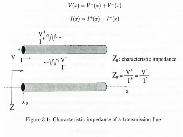
Characteristic impedance of a transmission line is defined as the ratio of the voltage and current wave phasors, that travel in the same direction. Better understanding of this definition can be obtained from Fig. 3.1.
The voltage at point x is :
K (x) = f/+ (x ) + V -(x ) I{x ) = I+ {x) - I~{x) V Z )
-: characteristic impedance
C
I
♦ XoFigure 3.1: Characteristic impedance of a transmission line
lo
< m l· .1,
IV2
L/2
Vl Z,(®)- { M )
( m . L/2< m y
<wyh-infiniteFigure
3
.2
: Infinite section artificial transmission line Then, the impedance seen from point x is,V {x) _ V+{x) + V -{x ) Z (x ) =
I(x ) I* (x ) - I - ( x )
If we prevent backward going voltage and current waves(V^~(x) = 0 and I~ {x ) =
0
), then we will have the impedance seen from point x equal to the characteristic impedance of the line.V*{x) + V-{x)
,
,
* “
I*(x) - I-(x) ~
Assume an excitation at point Xq. To find the characteristic impedance of
the line we can take the transmission line infinitely long, such that V'^ and /■'■ do not reflect, and measure the input impedance of the line. Or at least we can take the transmission line so long that reflected waves does not arrive at point xq before we measure the input impedance. In this case F “ (a;o) and I~{xo) are zero and, the input impedance seen from point xq is equal to the characteristic impedance of the line. We can now make another definition of the characteristic impedance : Characteristic impedance of a line is the input impedance o f the line, if it is infinitely long.
We can apply this definition to constant-k artificial transmission lines to find their characteristic impedance : If the artificial transmission line in Fig. 3.2 is infinitely long then the impedance seen from node A must be equal to the characteristic impedance of the artificial line. According to the same assump tion, node B is indifferent from node A, that is, the impedance seen from node B is also equal to the characteristic impedance of the line. Shortly,
Figure 3.3: Characteristic impedance of an artificial transmission line Writing KVL and KCL equations,
7
. . K4 V . . Lio
^0
^Vi = Zo{u>) j u —\X / i ,
/o — / i + jioCVi,
we can solve for Zq{uj) in terms of L, (7, and a;, which is,
(3.1)
A normalized plot of this function with respect to 2uj!uc is given in Fig. 3.3, where Uc —
2fy/ZC
is the cut-off frequency of the line. Up to this frequency, the characteristic impedance of the artificial line is purely real. At cut-off, the impedance is0
, and beyond the cut-off the impedance of the line is purely imaginary.As we are viewing this constant-k network as an artificial line, it must also have a well-defined phase factor. Determining the phase of a several section
Zin
L/2
< m y >
L
/2
Z
lFigure 3.4: Single section constant-k network
artificial line is very hard, but calculating the phase of a single section artificial line and multiplying it by the number of sections is a very easy way. Assume a single section artificial line terminated with an impedance as in Fig. 3.4.
Viewing this constant-k network as an artificial line with a characteristic impedance Zo(oj) and phase we can write the input impedance of this constant-k network using the well-known impedance transformation formula.
Zin — ZoZl + jZotan{^l)
Z o + jZLtan{^l) (3.2)
If we take Zl = 0 and calculate the input impedance o f the constant-k network, using KVL and KCL, w'e find :
Zin — j<^L
I —
u)
2LC= jojC
If the input impedance o f this constant-k network is calculated using the impedance transformation, putting Zl = 0 we get :
Zin = jZo{uj)tan^{u)
Equating the two Z,„ expression gives us the phase delay o f a single section artificial line.
$ (o;) = tan ^ \ujC
Zq{uj)
3.2
Resistive Artificial Lines
In distributed amplification, the input and output capacitances of the FETs are combined with inductors to form artificial transmission lines. The input and output impedances of the FETs are not pure capacitors, as mentioned in the previous chapter. The input capacitance contains a series resistance and the output capacitance contains a parallel resistance with it.
In M M IC technology only microstrip components are available and lumped element are not used. Because of this, building an inductor on a MMIC chip is a matter of concern. For large inductances, it is a real problem. For small inductances it is possible to build them via short lengths of high impedance microstrip transmission lines. To understand this remember the impedance transformation formula for transmission lines, Eq. 3.2. This equation gives the impedance seen from one of the ports of the line if the other port is terminated with a load Zi. Length and propagation constant of the line is / and /?, respectively. If Zl < < Zq, then
^in = Zl+ jZotan(^l)
If the length of the line is short(/ < \gf7)^ then tan(/SI) can be approximated with /31.
Zii„
=jZoffl
=jZ o -l
= X Iu c
Then, we’re left with an inductor whose inductance value is given by
C
A short length of transmission line can not be approximated with a single inductor. In fact, we have the approximation in Fig. 3.5, and corresponding equations, which are valid to a great extend for I < A^/7. [
12
](3.4)
c
Z
q
(3.5)Figure 3.5: Short length of transmission line I : length of the microstrip line
Zo : characteristic impedance of the microstrip line Cg// : effective dielectric constant of the medium c : speed of light
\g : wavelength at the highest frequency of interest
The value of the capacitance in the inductor approximation comes from the fact that, the impedance of a transmission line, Zo, is given by y T / C , where L and C are inductance and capacitance per unit length of line.
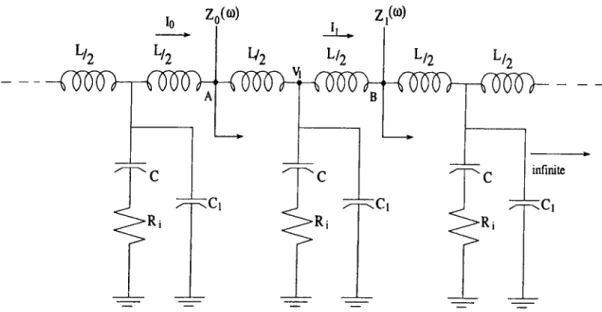
Including the input and output resistances of the FETs and the parasitic capacitances introduced by the inductors, the basic structure of an artificial transmission line, shown in Fig. 3.2, must be modified to give the artificial lines in Fig. 3.6 and Fig. 3.7. They represents the input and output artificial lines, respectively.
Using the same method, used in the previous section, we can find the impedance of these lines. In Fig. 3.6, Ci represents the capacitor of the in ductor approximation. The impedance of this line is then found to be.
Zo = where. (3.6) Ct = C C\, CCi a ' c + c v 1 -f- jcoC Hi 1 -f- juiC2Ri where C2 is the series of two capacitors, C and Ci.
L
/2
lo - a m Zn(®)c
>Ri Z,(®) L/2
L/2
- f i R R i V U W ) ;
:c,
c ‘ Ri^/2
L/2 - a m r - o m -X ,c
'Ri infinite -C ,impedance of the line. For the input line, also called gate-line^ C is the input capacitance of the FET, and Ci is the parasitic capacitance, so C is usually much larger than Ci and C
2
. Calling u>g = l/RiC and u>i = \IRiC2, we can say, u)g < u>i. Up to the frequency A{uj) can be approximated with1
, which gives us the previous result for the characteristic impedance given in Eq. 3.1. Below u>g, C is dominant to i?,· and we have a proper operation of the line. W hen frequency exceeds Ug, Ri becomes dominant to C. In this case, gate-line is very similar to the drain-line, and as will be seen later, for frequencies smaller than this artificial line will not be in proper operation. Beyond a>i, C\ will be dominant, and A{u>) can be approximated with (C -f C'i)/C'i, so at these frequencies the artificial line will have an impedance close to the impedance of the microstrip line we use. That is, safe and proper operation of this artificial line will be limited with ujg.For the output line, also called drain-line^ in Fig. 3.7, using the same method gives the following equation for the impedance of the line.
(3.7)
where Ct2 is the total capacitance, C -\-C\.
For Lo > u)d = IfRdsC, ju>L/{Gds jtaC) can be approximated as L/C, which gives us the known equation for the impedance.
Zo{^) — ¡ ± _ Ct2
Í1 - o ;2 LCt2\ (3.8)
For u! < u>d, the conductance of the capacitor is so low that Rd$ is dominant, and so the line is not an artificial transmission line. Over that frequency the capacitor becomes dominant, so the artificial line is in proper operation. In these kind of resistive constant-k networks, the artificial line approximation is good above a certain frequency,
ujd-Typically ujg is ~ 40 — 60 GHz and the gate-line operates below this fre quency. On the other hand, is ~
1
-2
GHz, and the drain-line operates above this frequency. Uc depends on the artificial line design, and the artificial lines operate below this cut-off frequency.3.3.1
Gate-Line
To obtain high input and output return-losses, gate and drain-lines should be designed to match the input and output port impedances. These impedances are usually 50 i), so the artificial lines should be 50 17 lines.
In order to have 50 17 artificial line, referring to Eq. 3.6, we must have
Cto 50 GTg = 2500 where,
CTg — Cg -f- C\ Cg ; input capacitance of the FET.
We also know, from Eq. 3.4 and 3.5, that «
62
X Ig G\~
63
X
where. Then,cZ,
og62
X
Ig Cg T 63X f0
= 2500 2500 ^ “62
- 2500 X63
’ (3.9) let61
= 250062
- 2500 X
63
,then ¡g = bi X Cgbi,
62
and&3
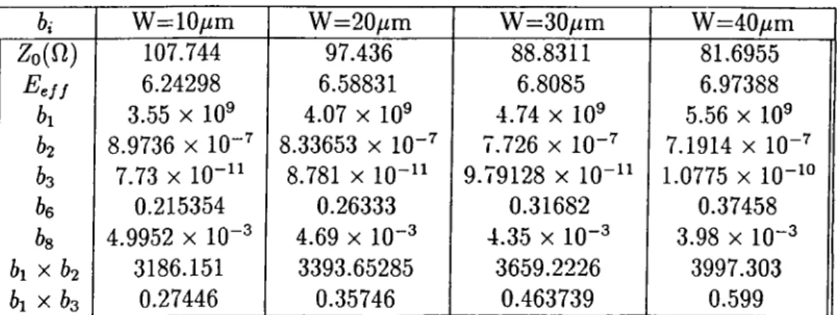
are dependent only on the microstrip line used. For the technology we use, Zq and Cg// are functions of the line width only. Cg//, in fact, has a slight dependence on frequency but it may be ignored for this moment. We shall just take the value of Cg// at the mid frequency. So, Eq. 3.9 gives the length of the microstrip line required to link the input capacitance Cg, to form a 50 12 artificial line.6
. W =10^m W =20
/im W =30/im W =40/im Zo(fi) 107.744 97.436 88.8311 81.6955 EefJ 6.24298 6.58831 6.8085 6.9738861
3.55 X 10^ 4.07 X 10^ 4.74 X 10® 5.56 X 10® h 8.9736 X 10-·^ 8.33653 X 10-^ 7.726 X 10-^ 7.1914 X lO-i' bs 7.73 X 10"^^ 8.781 X 10⁻¹^ 9.79128 X 10⁻¹¹ 1.0775 X 10⁻¹® be 0.215354 0.26333 0.31682 0.37458 bg 4.9952 X 10⁻³ 4.69 X 10⁻³ 4.35 X 10⁻³ 3.98 X 10⁻³ b\ X62
3186.151 3393.65285 3659.2226 3997.30361
X63
0.27446 1 0.35746 0.463739 0.599Table 3.1: List of
6
, values for 4 different microstrip-line widthTo see how the gate-line behaves,
Cg X Cl
¿1
X63
, ^ Cg + Ci 1 + 6x X h ^ let67
= 1 -1-(¿1
X 63) and be — bi x63/67
then,C2 = beX Cg
Cxg = bj X Cg
From the analysis of the resistive artificial lines we know that, some critical and important frequencies in the operation o f the line are given by:
where. / . = ^ =
1
2ir 2-K X R i X Cgf = ':!^ =
^
= — f
^ 2% 2 ir X R { X C2
be ^ f _ ^ ________2
^27T
2tt X y j L C j g^9
6
« — 1 7T\/6i X62
X67
All these
6
, values depend only on the microstrip-line used, and they tell us the appropriate line width to use. For four different line-widths, in other words, for four different characteristic im.pedance and effective dielectric constant pair, a list of6
, values is given in Table 3.1.For a given FET, i.e for given Cg and /2,. bi shows the length of the microstrip-line required to link Cg to give 50 i), bs gives the cut-off frequency o f the artificial line. As it it clear from the table, as line width increases, required length for the microstrip-line also increases, and the cut-off frequency o f the artificial line decreases. So it is best to chose the line width as small as possible. The disadvantage of narrow microstrip-line is the attenuation that will occur due to the finite conductance of the metallisation, and besides the line may not handle the current that is supposed to flow through. For the technology we are concerned, which is GEC-Marconi’s F
20
process,10
micron is the minimum allowable width, and this width of line is capable of carrying 50mA current. Since we are concerned with the gate-line, in which the signal level is low and no significant bias current flows, it is best to chose the line- width as small as possible.It is also clear that, required microstrip-line length is directly, and the cut off frequency, /c, is inversely proportional to the gate capacitance, Cg. On the other hand, a critical frequency, / i , is inversely proportional with both R{ and
Cg. That is, if possible, it is also best to chose a FET that has small /?,· and Cg parameters, as far as the frequency operation of the gate-line is concerned.
The artificial lines should be terminated with resistive loads so that un wanted signals dissipate at the end of the line. As the artificial lines are de signed to be 50 17 lines, these lines should be terminated with 50 17 resistors. In this case the impedance seen from the input of the gate-line will be 50 17 and the input return loss will be very large, i.e there will be negligible reflection to the source.
Remember that the characteristic impedance of an artificial line is frequency dependent and given by Eq. 3.6. It is hard to predict the behaviour of this func tion, but when bi values are investigated, it can be seen that fi{=l/2iTRiCg) is always much greater than fd^^sjC g), since R,· is always a small resistance. So, before A(o;) begins to effect the behaviour of the impedance, the artificial line reaches it’ s cutoff frequency. Depending on this reasoning, for the frequencies o f the proper operation o f the artificial line, we can safely take A(a;) equal to
1
. Then, we are left with the Eq. 3.1. Still the impedance of the line is frequency dependent and perfect match appears only at a single frequency. For the rest o f the frequency range input return loss is finite. In fact, for a real system it is not possible to obtain infinite return loss, there is always a mismatch some where, so rather than trying to obtain a perfect match it is essential to aim a limited return loss. Conventionally this limit for these class o f amplifiers is ~ 10 dB which corresponds to a VSW R of 1.925.Now, assume the artificial line to be terminated with a frequency dependent resistor whose value is equal to the characteristic impedance of the artificial line at all frequencies, up to the cut-off frequency. Then, the reflection coefficient is given by (for a 50 reference),
_ Zq{ijj) - 50 “ Zo{uj) + 50
If we limit the input return loss to be greater than 10 dB then we put a tolerance on Zo{uj)·
- 2 0 % I r I > 10 ^
/05
I r I < —0.51 r I < 0.316
Before cut-off, Zo{oj) is pure real, then we have the following tolerance for Zo(u>).
26 < Zo{u) < 96
(3.10)
When the artificial line is designed to be 50 fl, according to the plot3
.3
, Zq{uj) will be in a acceptable region up to86
percent of its cut-off frequency. Moreover, we can design the line to be a 96 ÎÎ line. In this case Zo{u>) will be in the tolerance band up to 96 percent of it’s cut-off frequency.The important problem, here, is the unrealistic termination resistor. When the termination is done with a usual resistor, the reflection coefficient may grow undesirably, and decrease the bandwidth of the artificial line. For exam ple, when the artificial line is designed to be
50
fi and terminated with a50
il resistor, at0.85/c,
input return loss may decrease to4.5
dB. Because o f the complicated phase expression of an artificial line, it is really hard to say what will happen, but, intuitively, safe regions, or in other words, large bandwidths are obtainable. For example, designing the line to be50
and terminating it with a smaller resistor around40
i) will probably give a bandwidth extending up to0.85/c.
Taking the termination resistor as50
17 and designing the line to be greater than50
17 may even extend the bandwidth over0.9/c.It
is not possible to find an optimum value for the resistor, but it is good enough to take intuitive values using the Smith-Chart and leave the rest to the optimizer. Onemore thing is that, designing the line with high impedance may seem charm ing but remember that high impedance artificial lines are hard(impossible in some cases) to build. More important, to increase the impedance requires an increase in the linking inductance, which also means a decrease in fc, so it may not help, or even make things worse. At this point, it is also clear that, decreasing the artificial line impedance(although this decreases the usable per centage o f fc, by increasing fc) may increase the bandwidth. Although an optimum termination resistance is hard to compute, it is possible to obtain an optimum line impedance to give the maximum possible bandwidth for a given input capacitance, which will be handled next.
Before going further, let’s have a look at the MESFET characteristics of GEC-M arconi’s F20 process. The linear model for these FETs are the same as given in Fig. 2.4 and the data is supplied by the same foundry. This process allows
2
, 4 and6
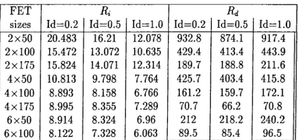
fingered FETs. In fact, any number of fingers can be used, but data is available only for those FETs. The model parameters are fully scalable in terms of the bias current and finger width. These scaling equations are given in Appendix A.These FETs do not have a simple series RC at the input. It is more com plicated than that, but when the input impedance of a FET is calculated for various frequencies, it is seen that the input port can be modeled as a series RC network whose capacitance and resistance values are frequency dependent. This calculation is done for 3 different finger number, 3 diflPerent finger width and
3
different bias current and the equivalent input capacitances are plotted. The 3 different finger widths are 50,100
and 175 microns, and 3 different bias currents are 20, 50 and 100 percent of the saturation current. The equivalent input capacitances for 2-fingered,4
-fingered and6
-fingered FETs can be seen in Fig.3
.8
, 3.9 and 3.10, respectively. The plot for the6
-fingered FET of 175 mi cron width (6x175) is omitted since the input capacitance exceeds 1 pF which is useless for our amplification purposes. The equivalent input resistances of these FETs do not vary too much with frequency, so the mid-frequency value is given, as a single value, in Table 3.2.As it is clear from Fig. 3.8, 3.9 and 3.10, equivalent input capacitance of these FETs are all frequency dependent. For 2-fingered FETs, small gate- width gives small and almost constant input capacitance. As the gate-width increases, the input capacitance and the dependence of the input capacitance on frequency increase. For
6
-fingered FETs this dependence is maximum. So, aside from the fact that the impedance of an artificial line is frequency de pendent, the capacitances employed in this artificial line are also frequencyFigure 3.8: Equivalent input capacitances for 2-fingered FETs
Figure 3.10: Equivalent input capacitances for
6
-fingered FETsFET
sizes
Id=0.2
Ri
Id=0.5 Id=1.0 Id=0.2
Rd
Id=0.5 Id=1.0
2x50
20.483
16.21
12.078
932.8
874.1
917.4
2x100
15.472
13.072
10.635
429.4
413.4
443.9
2x175
15.824
14.071
12.314
189.7
188.8
211.6
4x50
10.813
9.798
7.764
425.7
403.4
415.8
4x100
8.893
8.158
6.766
161.2
159.7
172.1
4x175
8.995
8.355
7.289
70.7
66.2
70.8
6x50
8.914
8.324
6.96
212
218.2
240.2
6x100
8.122
7.328
6.063
89.5
85.4
96.5
dependent.
As a summary, to design an artificial transmission line with a characteristic impedance of 50 ii it is enough to chose a capacitance value, then the length o f the microstrip line (value of the inductance) that will link the capacitances is automatically determined using Eq. 3.9 and Table 3.1. When a FET is employed in an artificial transmission line, that is when the input capacitance o f the FET is used as the capacitor of the line, the situation is a little bit different. Since the input capacitance of a FET is frequency dependent the question is which capacitance value to use as the reference value. That is, shall we take the low-frequency or high-frequency or mid-frequency value as a reference and apply to the Eq. 3.9? We may even take a completely arbitrary value as a reference (which is, in fact, equivalent to designing an artificial line o f impedance different from 50 il). All of these alternatives are possible and valid, but note that, in all cases the artificial line is not an 50 i) line. So, it is again emphasized that the problem is to find a reference capacitance value that maximizes the usable frequency band of the artificial line, rather than designing a 50 i) artificial line. This reference capacitance value is important in the sense that different choices lead to different bandwidths, and there is an optimum value for it.
Let Cq denote the reference capacitance value that is applied to Eq. 3.9, and C denote the frequency dependent input capacitance of the FET. Also define the bandwidth of the artificial line to be the frequency range where the input return loss stays equal or above 10 dB. Then, at the high frequency end o f the bandwidth, we can write the relation.
where.
f ^ /l OC
Ct = bi X
¿3
X Co C L = b i x b2 X CoLetting Lo —
27
t/ , we can write / in terms of C and Co- For10
-micronmicrostrip line width / is given as below :
1 , /OOOO.eCo - 676C
’ " C ' C ' i 27.5Co + 100.2C
(3.11)
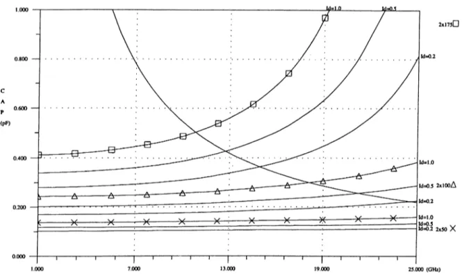
where / is in GHz and C and Co is in pFs.Remember that Eq. 3.11 is written for the high edge o f the frequency band, that is maximizing / for a fixed C maximizes the bandwidth too. This is done by taking the derivative of Eq. 3.11 and equating it to 0. From this, it is found that / reaches it’s maximum for Co = 0.43C. Substituting Co = 0.43C in Eq. 3.11 we get the maximum frequency of operation (MFO) curve.
/ = 5.446 (3.12)
This function is readily plotted on Fig. 3.S, 3.9 and 3.10. The intersection point of each FET’s input capacitance curve with this plot gives the maxi mum frequency of operation of the artificial line that can be build with the corresponding FET. For example, for a 2x100 FET with 100 percent bias, the intersection occurs at (18.25 GHz,0.298 pF). With this FET we can build an artificial gate-line whose maximum frequency o f operation is 18.25 GHz, pro vided that Co = 0.43 X 0.298 pF=0.128 pF is chosen as reference value to be
used in the Eq. 3.9. This curve can easily be used in deciding which FET to use, since it gives the maximum frequency of operation at the first glance.
Note that, when Co = 0.43C is used as the reference value, the impedance o f the gate-line is no more 50 0 . Even at low frequencies the impedance of the line is about 40 ii. One advantage o f this low-impedance artificial line is that, the variation of the gate-line impedance is between 26 fi and 40 fi, so that with a single resistance a good termination can be achieved at the end of the gate-line, due to the comparably small variation in the gate-line impedance. Also there may exist an optimum termination resistance that slightly extends the bandwidth. Trying to find this optimum value is a little bit complicated and not practical because, it is quite clear that this value will be around 40 i) and it will be very easy for a computer to find an optimum. And this completes the design of the gate-line.
Before going on, remember that Eq. 3.11 and
3.12
are process dependent and valid only for GEC-Marconi’s F20 process. Furthermore, they are calcu lated for10
micron line width and the coefficients in these equations change with the line width used. For20
, 30 and 40 micron line widths, Eq. 3.11 takes the form., 1 /3 1 5 0 C o -
676C
,,,
SaSOCo - 676(7
61.3(7o + 132(7
Vr = 30
f im (3.14)3590(7o - 676(7
94.5(7o + 158(7
W = 40 fim (3.15)For fixed (7, these functions reach their maximum, for Co = 0.41(7, Co = 0.38(7 and Co = 0.35(7, respectively. When these are substituted in Eq. 3.13, 3.14 and 3.15, MFO curves for
20
, 30 and 40 micron line widths are obtained, respectively as follows. f = f = f = 5.31 (7 (3.16) 5.15 (7 (3.17) 4.99 C (3.18)These curves also show that using wider microstrip lines decrease the cut off frequency of the artificial lines. Other curves for different line widths can also be derived.
3.3.2
Drain-Line
Before investigating the design procedure for the drain-line, we must have a look at the equivalent output admittance of Marconi’s FETs. For the FETs mentioned earlier equivalent output capacitances are plotted on Fig. 3.11, 3.12 and 3.13, and the equivalent output resistances (at mid-frequency) are tabu lated on Table 3.2.
For a constructive addition of the signals at the output terminal, phase shifts of the single section gate and drain-lines must be equalized. Recall that.
which can also be written as
A/ N <. -1 I rrF> \/l ^ _ i ( 2 - ( x ) \/l - { ^ l ^ c Y
$(u;) = tan I tx)v LC X --- „ jf-r
1
= tan ^I
--- x —--- ;— ;— —■where o>c = 2 /v /Z C . Then, if we want the phcise shifts of the gate and drain lines to be equal, it is enough to equalize the cut-off frequencies of these lines.
i0^.a = = =
y/L^d
If, also, gate and drain-line impedances are made equal.
then we are left with the strict condition that Lg = Ld and Cg = Cd· As it is clear from Fig. 3.8 and 3.11, the input and output capacitances of the FETs are not equal which readily violates the condition Cg = Cd- To avoid this, a small capacitance is added at the drain terminal of each FET just to compensate the difference between the gate and drain capacitances of a FET.