T.R.
DICLE UNIVERSITY
INSTITUTE OF NATURAL AND APPLIED SCIENCES
ELECTRICAL AND PHOTOELECTRICAL
CHARACTERIZATION OF Au/ZrO
2/n-Si MIS
CONTACT
Masoud Giyathaddin OBAID
MASTER THESIS DEPARTMENT OF PHYSICS
DİYARBAKIR June 2015
T.R.
DICLE UNIVERSITY
INSTITUTE OF NATURAL AND APPLIED SCIENCES
ELECTRICAL AND PHOTOELECTRICAL
CHARACTERIZATION OF Au/ZrO
2/n-Si MIS CONTACT
Masoud Giyathaddin OBAID
SUPERVISED BY
ASSOC. PROF. DR. YUSUF SELIM OCAK
MASTER'S THESIS DEPARTMENT OF PHYSICS
DİYARBAKIR June 2015
i
Acknowledgement
First I extend the big thank to the God for completing this thesis, and then I am highly thankful to my supervisor Assoc. Prof. Dr. Yusuf Selim Ocak, who gave me his precious time, valuable advices, good ideas for choosing the subject of the thesis and illuminating the way to me for completing the research and gave me the suitable plans for completing the thesis in the best way. Also I offer my thanks to Dr.Ahmed Tombak who work in Institute of Natural and applied sciences in Dicle University for his helping to me especially in the laboratory when I performed experiments. Also I offer my thanks to Assoc.Prof. Dr. Omer Celik who works in Institue of natural and applied sciences in Dicle University for his helping and advices to me for compliting the thesis.
My thanks also go to Dr.Nazar the dean of college of engineering in Duhok University for his supporting and encouraging to me to complete master degree.
Also I offer my thanks to Mr. MohamedMahdi MohamedSalih who work in the library of college of science in Duhok University who helped me for borrowing beneficial books related to my thesis.
Also I extend my heartily thanks to my mother, father, wife, and my dear son Siraj and my dear daughter Sanaz for encouraging me to do this work.
Also I am gratefully thanks my friends and my colleagues in Dicle university for their helping to complete this thesis.
ii CONTEXT Title Page Acknowledgment i CONTEXT ii ÖZET iv ABSTRACT v LIST OF TABLES Vi
LIST OF FIGURES Vii
LIST OF ABBRIVIATION ix
1. INTRODUCTION 1
2. LITERATURE SUMMARY 3
3. MATRIAL AND METHOD 9
3.1 Metal-Semiconductor Contacts 9
3.1.1 Rectifying Contacts 10
3.1.2 Ohmic Contacts 11
3.2 Physical Vapor deposition Methods 12
3.3 Optical Properties of Materials 13
3.3.1 Absorbance 13
3.3.1.1 Direct band transition 15
3.3.1.2 Indirect band transition 16
3.3.2 Transmittance 16
3.4 Experimental procedures 19
3.4.1 Formation of ohmic contact 19
3.4.2 Deposition of ZrO2 thin film 20
iii
4. FINDING AND DISCUSSION 23
4.1 Introduction 23
4.2 Optical properties of ZrO2 Thin Film on quartz 23
4.3 Current-voltage properties of Au/ZrO2/n-Si MIS diode 25 4.4 Photoelectrical properties of Au/ZrO2/n-Si MIS diode 28 4.5 Capacitance-voltage properties of Au/ZrO2/n-Si MIS diode 29
5. RESULTS AND SUGGESTION 33
6. REFERENCE 35
iv ÖZET
Au/ZrO2/n-Si MIS KONTAĞIN ELEKTRİKSEL VE FOTOELEKTRİKSEL
KARAKTERIZASYONU
YÜKSEK LİSANS TEZİ
Masoud Giyathaddin OBAID
DİCLE ÜNİVERSİTESİ FEN BİLİMLERİ ENSTİTÜSÜ
FİZİK ANABİLİM DALI
2015
Metal yalıtkan yarıiletken (MIS) kontaklar birçok yarıiletken aygıtların en önemli bileşenlerinden biridir. Günümüzde klasik SiO2 kapı oksiti yerine yüksek dielektrik sabite sahip yalıtkan tabakaların kullanılması çokça çalışılmaktadır. Zirkonya geniş band aralığı (5-8 eV) ve yüksek dielektrik sabiti (ε ≈ 25) ile bu amaç için en önemli adaylardan biridir. Bu çalışmada, Au/ZrO2/n-Si MIS yapısı ZrO2 ince filminin n-Si alttaş üzerinde büyütülmesi ve ince film üzerine Au buharlaştırılması ile oluşturulmuştur. Au/ZrO2/n-Si MIS yapısının elektrik ve fotoelektrik karakterizasyonu oda sıcaklığında karanlıkta ve farklı ışık şiddetinde alınan akım-gerilim (I-V) ölçümleri ile belirlenmiştir. Ayrıca, Au/ZrO2/n-Si MIS yapısının kapasite-gerilim (C-V) karakteristiği incelenmiş ve her iki yöntem ile elde edilen engel yüksekliği değerleri karşılaştırılmıştır.
v ABSTRACT
ELECTRICAL AND PHOTOELECTRICAL CHARACTERIZATION OF Au/ZrO2/n-Si MIS CONTACT
MSc THESIS
Masoud Giyathaddin OBAID
DEPARTMENT OF PHYSICS
INSTITUTE OF NATURAL AND APPLIED SCIENCES UNIVERSITY OF DICLE
2015
Metal insulator semiconductor (MIS) contacts are key components for many semiconductor devices. The usage of high dielectric constant (high-) insulator layers instead of conventional SiO2 gate oxide is currently widely studied. Zirconia with very large band gap (5-8 eV) and high dielectric constant (ε ≈ 25) is one of the most important candidates for this purpose. In this study, Au/ZrO2/n-Si MIS structure was fabricated by deposition of ZrO2 thin film onto n-Si substrate and evaporating the Au metal onto thin film. Electrical and photoelectrical characteristics of Au/ZrO2/n-Si MIS structure were analyzed using its current-voltage (I-V) measurements at room temperature in dark and under a solar simulator for various illumination intensities. In addition, capacitance-voltage (C-V) characteristics of Au/ZrO2/n-Si MIS structure were studied and the barrier heights obtained from both measurements were compared.
vi
LIST OF TABLES
Title Page
Table 4.1.Some electrical parameters of Au/ZrO2/n-Si MIS device at room temperature
27
Table 4.2. Photoelectrical parameters of Au/ZrO2/n-Si MIS device at room temperature
vii
LIST OF FIGURES
Title Page
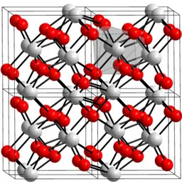
Fig.1.1 Crystal structure of ZrO2 1
Fig.2.1 The proposed illustration of potential of surface and interface stapping in MIS GaAs diode by Hudait el al
4
Fig. 2.2 C-V curves of Al/Y2O3/n-Si showing hysteresis effect 6 Fig. 2.3.a) MIS diode I-V measurement of Al/TiO2/n-GaAs, Al/Al2O3/TiO2
/n-GaAs, Al/HfO2/TiO2/n-GaAs
7
Fig. 2.3.b Rc-dielectric thickness using TiO2, Al2O3 and TiO2 +Al2O3 7 Fig. 3.1 Energy band diagram of metal-n-type semiconductor a) before the Formation of a contact b) after formation of a contact
11
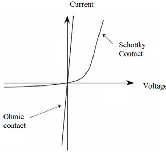
Fig. 3.2. Ohmic and Schottky contact plots 11
Fig. 3.3. Diagrams of sputtering and thermal evaporation processes 13
Fig. 3.4 Absorption in a thin film 14
Fig. 3.5 Representation of the direct and indirect transition through band gap 14
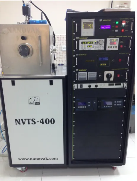
Fig. 3.6 The annealing furnace used in the study 19
Fig. 3.7. Nanovak NVTS 400 vaccum system 20
Fig. 3.8. The cross section illustration of Au/ZrO2/n-Si MIS diode 21 Fig. 3.9.a. Current-voltage measurement system with Keithley 2400
sourcemeter and Oriel solar simulator
21
Fig.3.9.b. Capacitance-voltage measurement system with Agilent 4294 A Impedance analyzer
22
Figure 3.10. Shimadzu 3600 Uv-vis-nir spectrophometer 22 Fig. 4.1. Absorbance vs. wavelength plot of ZrO2 thin film on quartz 23 Fig. 4.2. (Ah)1/2-h plot of ZrO2 thin film on quartz 24 Fig. 4.3. lnI-V plots of Au/ZrO2/n-Si MIS diode in dark and various illumination conditions
viii
Fig. 4.4. Norde plot of Au/ZrO2/n-Si MIS diode 27
Fig. 4.5. C-V plots of Au/ZrO2/n-Si MIS diode at various frequencies 30 Fig 4.6. C2-V plots of Au/ZrO2/n-Si MIS diode at various frequencies 30
ix LIST OF ABBRIVIATION
Abbreviation Meaning
MS Metal-Semiconductor
MIS Metal-Insulator-Semiconductor
I-V Current-voltage characteristics
ZrO2 Zirconium oxide
HF Hydrofluoric acid
H2SO4 Sulfuric acid
MOS Metal oxide semiconductor
High High dielectric
SiO2 Silicon dioxide
ε Dielectric constant O2 Oxygen molecule
Au Gold
C-V Capacitance-voltage
epi-GaAs Epitaxial Galium Arsenide
β-Ga2O3 Beta Galium Oxide
SnO2 Tin Oxide
MB Methylene blue
AC Alternating current
TiO2 Titanium Dioxide
DC Direct current RF Radio frequency Al Aluminum Y2O3 Yttria Ta2O2 Tantalum oxide Al2O3 Alumina
x
HfO2 Hafnia
FET Field effect transistor
MOSFET Metal oxide semiconductor field effect transistor
Nb2O5 Niobium oxide
ALD Atomic layer deposition
UV Ultra violet
PVD Physical vapor deposition
Φm Work function of metal
Φs Work function of semiconductor
qx electron affinity
Φb Barrier height
Φbn Barrier height of n-type
Φbp Barrier height of p-type
Eg Energy band gap
E Intensity of light passing through the thin film
E0 Intensity of incident light
I Current V Voltage q Electron charge n ideality factor k Boltzman constant T absolute temperature RC Contact resistance
CVD Chemical vapor deposition
x thin film thickness
α Absorption coefficient
xi
ʋ Frequency
Ei Initial energy state
ES Final energy state
me effective mass of the electron
mh effective mass of the hole
Eph phonon energy
R Reflectance
n refractive index for semiconductor
no real part of refractive index
k imaginary part of refractive index
A diode area
A* Richardson constant
F(V) Norde function
F(V0) minimum value of Norde function
Rs Series resistance
K Kelvin
Cu Cupper
PSP Phenolsulfonphthalein
Voc Open circuit voltage
Isc short circuit current
εs Dielectric constant of semiconductors
p-Si p-type of Silicon n-Si n-type of Silicon
αs Absorption coefficient
MASOUD GIYATHADDIN OBAID
1 1. Introduction
Nowadays, semiconductor technology covers all our lives. Nearly all electrical and optoelectronic devices mainly formed using semiconductors. Metal-semiconductor (MS) and metal-insulator-semiconductor (MIS) junctions are key components for many semiconductor devices including microwave applications, photodiodes, physical, chemical and biological sensors. MIS contacts can be formed by inserting thin insulator layer between metal and semiconductor. This insulator layer converts MS contact to MIS diode. According to Sze (Sze and Kwok 2007) MIS junction is the most advantageous structure in the study of semiconductor surfaces.
Reliability and stability of electronic devices are mainly related to surface conditions. The main electrical parameters of MS and MIS diodes are barrier height, ideality factor, series resistance and interface states. These parameters can be determined by means of current-voltage (I-V) data in dark. It is well known that electrical characteristics of MS and MIS contact are strongly affected by the existence of an insulator layer.
Zirconium oxide (ZrO2) which is known as zirconia is one of most studied ceramic material owing to its thermal and chemical stability. The melting point of ZrO2 is 2715 °C. It has monoclinic crystal structure till 1170 °C and its solubility in water is negligible. It is soluble in concentrated HF and hot H2SO4. Because of its thermal and chemical stability, ZrO2 has been used as thermal barrier coater in jet and diesel engines. It has been also used to obtain durable dental prostheses. (wikipedia, 2015)
1.INTRODUCTION
2
MIS or metal-oxide-semiconductor (MOS) devices fabricated using high dielectric constant (high-k) insulator layers are currently widely studied for replacement of conventional SiO2 gate oxide. Zirconia with very large band gap and high dielectric constant (ε ≈ 25) is one of the most important candidates for this purpose. ZrO2 has a large optical band gap between 5-8 eV. It means that it a stable insulator and it can be used in the fabrication of highly stable electronic devices.
There are many ways to obtain a thin film of materials including spin coating, ultrasonic spray, thermal evaporation, pulsed laser deposition, electron beam, cathodic arc deposition and molecular beam epitaxial. It is very difficult to form thin films of refractory metals or ceramics. Magnetron sputtering technique is a unique method to obtain uniform thin films of ceramics refractory metals or ceramics.
In this study, it was aimed to fabricate MIS diode using ZrO2 as high-k insulator and determined its electrical and photoelectrical properties. For this aim, ZrO2 thin film was growth on n-Si semiconductor by reactive sputtering technique. Zr metal was used as target and O2 was used as reactive gas. To increase crystallianity, ZrO2 thin film was annealed at 500 C for 30 minutes in air ambient. Au metal was evaporated to obtain front contact. Electrical and photoelectrical characteristics of Au/ZrO2/n-Si MIS structure were analyzed using its current-voltage (I-V) measurements at room temperature in dark and under a solar simulator for various illumination intensities. In addition, capacitance-voltage (C-V) characteristics of Au /ZrO2/n-Si MIS structure were studied and the barrier heights obtained from both measurements were compared.
MASOUD GIYATHADDIN OBAID
3 2. Literature Summary
The first electronic device was fabricated by Braun in 1874 (Mönch 2013). He found the asymetry in electrical conductivity of metal/semiconductor (MS) contacts formed using metal sulfate crystals. Pickard invented first MS detector and took its patent in 1906. Pierce showed the rectifiction behavior of MS contact which was formed on the surface of the semiconductor with metal wires.
The first principal study on rectifying properties of MS contact was performed by Schottky, Sörmer and Waibel in 1931. According to them, rectification can be explained because of the potential drop across all contacts when current flows in the contact (Schottky, Stormer et al. 1931). After this study, Wilson developed the theory of quantum mechanical tunneling and explained the rectification using reverse polarity.
1938, Schottky and Mott independently suggested that rectification mechanism can be explained electron flows and diffusion over potential barrier. According to Schottky-Mott theory, existence of potential barrier is result in differences between metal and semiconductor work functions. Thus, greatness of potential barrier can be calculated using the differences between metal work function and semiconductor electron affinity. But, the experiments showed that barrier height is approximetly independent from metal work functions and its related to preperation methods. It was conculated from experimental results that theory was insufficient because it didn’t take the existance of a layer at MS interface into account. The fact that this layer is always possible in practice and prepration conditon can manipulate its thickness and
Monch argued that ideality factor and barrier height parameters can vary from diode to another diode owing to barrier height inhomogeneity (Mönch 1999). Barrier height values of homogenious MS contacts were expressed as 1.01 when image force lowering of Schottky potential taking into account. The effect of series resistance on forward bias current-voltage (I-V) characteristics for non-ideal Schottky contacts was investigated by Norde. In 1986 Cheung and Cheung proposed another method to calculated barrier height, ideality factor and series resistance values for both ideal and non-ideal diodes using their forward bias I-V characteristics (Cheung and Cheung 1986). It is the fact that except for very special fabrication condition, formation of a native oxide layer between metal and semiconductor is unavoidable. This insulator layer
2. LITERATURE SUMMARY
4
converts MS contact to metal-insulator-semiconductor (MIS) diode and it has strong effects on diode characteristics.
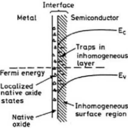
The first study on interface states of Schottky diodes performed by Cowley ve Sze (Cowley and Sze 1965). They executed the correlation between barrier height values and work function of metals, interface states and interlayer thickness. Hudait and Krupanidhi analyzed the effect of thin oxide layer in MS and MIS epi-GaAs Schottky diodes using -Ga2O3 as insulator layer (Hudait and Krupanidhi 2000). They calculated ideality factors and barrier height values as 1.16, 0,912 eV and 1.17 and 0.970 eV for epi-GaAs based MS and MIS contacts, respectively. They suggested that the reduction saturation current values for MIS diode is because of a thin insulator layer and the combination of increased barrier height and decrease in Richardson constant.
Figure 2.1 The proposed illustration of potential sources of surface and interface stapping in MIS GaAs diode by Hudait el al.
Gokcen et al fabricated Au/n-Si and Au/SnO2/n-Si MS and MIS contacts to see the effects of insulator layer and series resistance on forward and reverse bias I-V characteristics of devices (Gökçen, Altındal et al. 2011) . They reported that both MS and MIS structures had non-ideal diode characteristics because of existence of interface states, native interfacial layer and series resistance. They calculated electrical parameters of devices from ln(I)-V and Cheung methods.
MASOUD GIYATHADDIN OBAID
5
Ocak et al determined electrical and interfacial properties of Sn/Methylene Blue (MB)/p-Si structure using its I-V and capacitance-voltage (C-V) measurements at room temperature in dark (Ocak, Kulakci et al. 2009). They used ln(I)-V plots, Cheung functions 4 and modified Norde functions to obtain the ideality factor, barrier height and series resistance of diode. They reported that MB layer behaves as a physical barrier between metal and semiconductor and modifies barrier height of the structure. They also compared the barrier height results obtained from I-V data to one determined from C-V data. The results showed that in sufficiently high frequencies, the interface states can not follow the alternating current (ac) signals. They also calculated the interface state density of the structure using its I-V data.
Kinaci et al deposited titanium dioxide (TiO2) thin films on n-Si substrates using direct current (DC) magnetron sputtering method at 200 ⁰ C (Kınacı, Çetin et al. 2012). They annealed thin films to increase the crystal quality at 900 ⁰ C in air ambient. By this way they obtained rutile phase of TiO2 thin films. They used Au as front contact and they obtained Au/ TiO2 (rutile)/n-Si MIS rectifying diode. They calculated main electrical parameters including barrier height, ideality factor and series resistance values using I-V data obtained between 200 K and 380 K. They reported the increase in barrier height values and decrease in ideality factor values with increasing temperature. They also supposed to usage of rutile phase of TiO2 for device applications owing to low series resistance property.
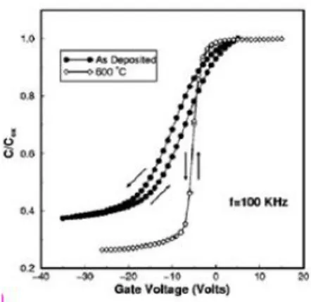
Yttrium oxide dielectric thin films were formed on n-Si wafer using RF magnetron sputtering system and annealed at various temperatures (400-600 ⁰ C) by Evangelou et al (Evangelou, Wiemer et al. 2003). Metal-oxide-semiconductor (Al/Y2O3/n-Si) structures were fabricated by evaporating thin Al metal on oxide layer. Hysterisis effects were reported in C-V curves for devices.
2. LITERATURE SUMMARY
6
Figure 2.2 C-V curves of Al/Y2O3/n-Sishowing hysteresis effect.
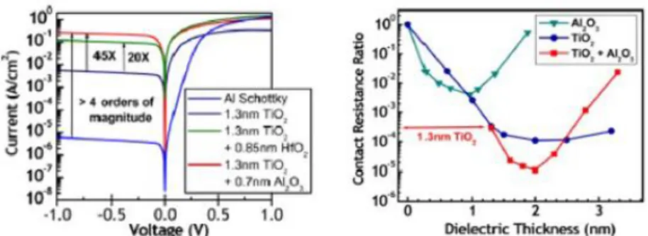
The physical thickness of ultrathin silicon dioxide films limits the silicon based dielectrics. Thicknesses lower than 10-12 Å, because of direct quantum mechanical tunneling unwanted high leakage current and breakdown of dielectric ar low voltages occurs. Therefore, new dielectric materials with high permittivity are necessary to reduce leakage current. Transition metal oxides including Ta2O5, TiO2, Al2O3, ZrO2, HfO2 are potential high-k dielectric matarials (Chang, Jeon et al. 2002). Chang et al deposited ZrO2 instead of SnO2 as the gate dielectric material by means of rapid thermal chemical vapor deposition for field effect transistor (FET) applications. They chose ZrO2 because of good thermal stability and large band gap. They obtained metal-oxide-semiconductor (MOS) capacitors which is ideal for MOSFETs with low leakage current, perfect C-V responses and low interface state density properties Oh et al growth Nb2O5 thin films on p-Si via pulsed DC sputtering with various oxygen flow rates (Oh, Kim et al. 2013). They reported that Al/Nb2O5/p-Si MIS structure obeyed Schottky emission mechanism. They also presented low noise characteristics Low frequency noise characteristics of Al/Nb2O5/p-Si diodes. Hu et al formed ultrathin dielectrics to reduce affectice barrier height of Al/n- GaAs. They formed HfO2, Al2O3, TiO2, ZrO2 and bilayer high-k dielectrics using atomic layer deposition (ALD) method. They showed effective barrier heigh and contact resistance tuning of Al/n-GaAs contacts using two high-k dielectrics in combination.
MASOUD GIYATHADDIN OBAID
7
Figure 2.3. a) MIS diode I-V measurements of Al/TiO2/n-GaAs, Al/Al2O3/TiO2 /n-GaAs, Al/HfO2/TiO2/n-GaAs and b) Rc-dielectric thickness using TiO2, Al2O3 and
TiO2+ Al2O3
In this study, electrical and photoelectrical characterization of Au/ZrO2/n-Si MIS contact were investigated. For this purpose, an ohmic contact for n-Si semiconductor was obtained forming a thin Au thin film on unpolished side of n-Si and annealing at 420 0C in N2 atmosphere for 3 minutes. ZrO2 thin film was deposited on n-Si/Au and quartz substrates by reactive sputtering of Zr metal target at room temperature. The ZrO2 thin film was annealed for an hour at 500 ⁰ C to increase the crystal quality. Optical properties of thin film were determined using UV-vis data. Ag front metal contact was formed by thermal evaporation method and by this way Au/ZrO2/n-Si MIS contact was obtained. Electrical parameters including barrier height, ideality factor and series resistance values were calculated using dark I-V measurements. The effects of light intensity on I-V characteristics of device were analyzed. Furthermore, the obtained barrier height value from I-V data compared the one calculated from C-V data.
2. LITERATURE SUMMARY
MASOUD GIYATHADDIN OBAID
9 3. Materials and Methods
In this study, Au/ZrO2/n-Si metal-insulator-semiconductor (MIS) structure was fabricated by reactive sputtering of Zr metal using O2 as reactive gas and evaporation of Au as front contact. Before the formation of the device an ohmic contact was formed on unpolished side of n-Si wafer by thermal evaporation of Au metal in a vacuum system. Electrical properties of the device were analyzed using current-voltage and capacitance-voltage measurements at room temperature in dark. The photoelectrical characteristics of the structure were examined using its current-voltage measurements under a solar simulator for various illumination intensities. Furthermore, the optical properties of ZrO2 thin film on quartz were determined using UV-vis data.
In this chapter, firstly the physics of MS and MIS structures, the conduction mechanisms in these contacts and the factors which affect physical parameters of devices will be given. Then, physical vapor deposition (PVD) systems which were used in this study will be discussed. Optical properties of materials will be also discussed in this chapter.
Finally, at the end of the chapter, all experimental parts of this study will be explained in detail.
3.1. Metal-Semiconductor Contacts
Metal semiconductor (MS) contacts have great importance because they are used in the fabrication of all kinds semiconductor based electronic devices. MS contacts can be examined in two different parts as ohmic contacts and rectifying Schottky contacts. In this part, formation of MS structures, conduction mechanisms of these structures and determination of electrical properties will be discussed.
When a metal and semiconductor make a contact without any material between them it is called as MS contact. Theoretically, if the work function of semiconductor is larger than the work function of metal (m<s), it forms rectifying contact and if the work function of metal is larger than the work function of semiconductor (s<m), it forms ohmic contact for p-type semiconductors. For the n-type semiconductor it is just the opposite (Rhoderick and Williams 1988).
3.MATERIALS AND METHODS
10 3.1.1. Rectifying Contacts
Work function of metal is expressed as qm and it is equal to q(χ+n) where qχ is electron affinity which defined as the difference between the bottom of the conduction band the vacuum level. The contact potential is defined as the difference between two work functions (m-(χ+n)). When the distance between metal and semiconductor is decreased, electric field in this region increases and decreasing negative carrier occurs. A positive carrier should be created at depletion region. The potential difference is very similar to one side of p-n junction. If the distance is very small, this region becomes transparent for electrons and the situation shown in Fig. 3.1 occurs. For an ideal contact between a metal and a p-type semiconductor, barrier height is written as
bnq m q 3.1
bpEg q m q 3.2Therefore, sum of the barrier heights of a MS contact formed using a metal and p-type and n-type semiconductor is equal to band gap of the semiconductors.
bp bn
g q
E 3.3
For a MS contact formed using an n-type semiconductor, ionized donors (positive carriers) in semiconductor side of contact are space charges because they are motionless. When a reverse potential applied to contact, barrier height doesn’t change for electrons which wants to pass to barrier. For this reason, current flow from semiconductor to metal becomes constant. On the other hand, for electrons pass from metal to semiconductor barrier height decreases about eV value and current flow from metal to semiconductor decreases as exp(eV/kT) factor. Therefore, the net current can be expressed as nkT IR V q I I 0exp ( s) 3.4
Where I is the current, I0 is the current q is the electron charge, V is the applied voltage, n is the ideality factor, k is the Boltzmann constant T is the absolute temperature. For this equation, net current is positive and this situation is called as forward bias. When a positive voltage applied to semiconductor, conduction band decreases about eV and barrier height in the semiconductor side increases about eV. This situation is called as reverse bias.
MASOUD GIYATHADDIN OBAID
11
Figure 3.1 Energy band diagram of metal-n-type semiconductor a) before the formation of a contact b) after formation of a contact
3.1.2 Ohmic contacts
The main aim to use ohmic contacts is to get or give current to semiconductor with minimum resistance. Ohmic contact obeys the ohm law. The quality of the ohmic contact is related to contact resistance. This resistance is written as
1 0 V C V I R 3.5
The comparison of ohmic and Schottky contacts are shown in Fig. 3.1.
3.MATERIALS AND METHODS
12 3.2. Physical Vapor Deposition Methods
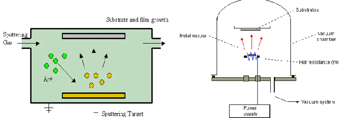
The main methods for depositing thin films are evaporations and sputtering, so the concentration will be on the explanation of these methods in this chapter. The aim which stands behind the process of deposition is to make a control on the transfer of atoms from the source to subtract where film consistence and outgrowth progress atomistically. During the process of evaporation, atoms are separated from the source due to thermal means but in the process of sputtering, they are expelled from solid target surface due to the effect of gaseous ions. The beginning experimentation of these kinks of deposition techniques can be obviously influence to same period of the nineteenth century. Grove in 1852 AC realize sputtering of metal deposits from cathode of an illumination discharge. Faraday after five years, testing with exploding fuse like metal in a static atmosphere, fabricated evaporated thin films. With the progress and evolution of vacuum pumping instrument and manufacturing of suitable Joule heating sources such as which made from platinum and tungsten wire, supported the progress of evaporation technology. The scientific advantage in the phenomenon of evaporation and the characteristics of thin films of metal was followed up by industrial output of optical components like beam splitters, mirrors, and antireflection coatings. Sputtering was utilized in 1877 to coat mirrors, and its usages included coating of flimsy construction with Au and deposition of metal films on record rules of phonograph records before to thickening Up to the late of 1960s, evaporation obviously exceeded sputtering as the favorite film deposition technique. Higher deposition average, superior vacuum, and cleaner environments for film consistence and outgrowth, and general usable to all categories of materials were some of the reasons for dominance of evaporation methods. Films are used for magnetic and microelectronic applications required the usage of alloys, with severe stoichiometry limits, which ought to adapt cover and abide well to substrate surfaces. These requests plus the introduction of radio frequency (RF), bias and magnetron varians that spread the power of sputtering and availability of high purity targets and working gases, assisted prefer the popularity of sputter deposition.
According to special implementations to evaporate or sputter thin films is not always clear and has encouraged a lively competition among these methods. On the other hand, characteristics of evaporate and sputter have been fabricated into mongrel operation. The basic film deposition methods treated in this thesis are physical vapor
MASOUD GIYATHADDIN OBAID
13
deposition(PVD), the expression that includes evaporation and sputtering, and chemical vapor deposition (CVD) will all of variant and mongrel operations.
The following are some factors which differentiate PVD from CVD 1. Dependence on solid or molten sources.
2. Physical techniques (evaporation or collisional affect) by which source atoms get in the gas phase.
3. Reducing pressure environment through which the gaseous sort are transported. 4. Overall nonattendance of chemical reactions in the gas phase and at the substrate
surface (PVD reactive processes are exclusion).
Figure 3.3. Diagrams of sputtering and thermal evaporation processes
3.3. Optical Properties of Materials 3.3.1. Absorbance
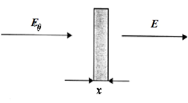
Absorption is called energy loss of an incident electromagnetic wave to a crystal plane by interacting with the electrically charged particles. The most commonly used method for determining forbidden energy band gap of semiconductors is optical absorption method. A photon coming to a semiconductor excites an electron from low energy level to a high energy level in absorption process. The correlation between incident and transmitting of beam light coming through the thin film with a thickness x is as follows
x
e E
E 0 3.6
where E0 the intensity of the incident light, E intensity of light passing through the thin film, x is thin film thickness and α is absorption coefficient of the material used (semiconductor).
3.MATERIALS AND METHODS
14
Figure 3.4 Absorption in a thin film
There are two types of band transition in crystalline and amorphous semiconductors. These are direct and indirect band transition and shown in the figure3.5. Direct transition state occurs when the momentum of minimum valance band is the same as conduction band momentum. In Figure 3.5, the electron absorbs a photon without a change in its momentum value and transmits from valence band to the conduction band with energy received from the photon.
Figure 3.5 Representation of the direct and indirect transition through band gap
The minimum valance band energy is different from that of the conduction band maximum energy for the material having an indirect band gap. Electrons in the conduction band go down to the minimum band energy quickly. In the same way, holes reach the maximum of valance band. Therefore, momentum of electrons and holes is the same for a direct transition semiconductor while is not the same for
MASOUD GIYATHADDIN OBAID
15
indirect transition semiconductor. This result is because of the lifetime of minority charge carriers and optical properties.
3.3.1.1. Direct band transition
When a photon with energy hν comes to a direct band gap semiconductor, an electron jumps from the valence band to the conduction band. Ei is initial state in semiconductor, Es is the final energy state. Therefore, the energy difference,
i
s E
E
h
3.7
is given by the equation. In the parabolic band,
* 2 2 e g s m p E E 3.8 and * 2 2 h i m p E 3.9
is determined by the expressions. Where me* the effective mass of the electron and mh* is effective mass of hole. If equations 3.32, 3.33 and 3.34 are arranged
2 1* 1* 2 e h g m m p E h 3.10
is obtained by correlation. In direct band transition relation between α and hν is; m g E h B h ( ) 3.11 is given by the equation. B is constant, m is a constant, which can take 1/2 for, allowed transition or 3/2 forbidden transition values. In addition, in equation 3.8 the value making zero of the parenthesis gives the forbidden energy gap value of the semiconductor which is equal to αhν.
3.MATERIALS AND METHODS
16 3.3.1.2 Indirect band transition
Because the momentum of the electrons of valance band maximum and conduction band minimum, in order to conserve momentum of the electrons, photon absorption event should contain additional particles. In this case, either emission or absorption of a photon for momentum conservation is required.
The phonon absorption coefficient
1 ) / exp( ) ( kT E E E h h ph m ph g s 3.12 and
) / exp( 1 ) ( kT E E E h h ph m ph g e 3.13can be written. Here sis absorption coefficient and eis emission coefficient, Eph is the phonon energy. It is also possible for both possibilities
) ( ) ( ) ( h s h e h 3.14
can be written. When it is clearly written
) / exp( 1 1 ) / exp( ) ( kT E E E h kT E E E h h ph m ph g ph m ph g 3.15Where m is a constant, which can take 2 allowed or 3 forbidden transition values for an indirect band gap semiconductor.
3.3.2. Transmittance
Transmittance is defined as the ratio of the intensity of light incident on the sample to the intensity of light passing through a sample and expressed by the equation
0
E E
MASOUD GIYATHADDIN OBAID
17
Both transmission and reflection from a medium depends on the refractive index and the absorption characteristics. Therefore, interactions are always not necessarily, not classified as reflection and absorption. Transmittance is clearly observed by absorbance of gases (excluding reflections from the reactor wall) (Herman, 1996). Optical transmittance or absorbance measurements are used to determine the optical absorption coefficient and specific impurities. Shallow level impurities correspond to optical measurements. Certain impurities have the characteristic absorption lines due to the vibrational mode; such as oxygen and carbon in the silicon. One of absorbed photons in semiconductor can make sudden environmental changes by producing local vibrational modes around certain impurities. During the transmittance measurements, light comes to sample and transmittance is measured as a function of wavelength. The reflection coefficient of the sample, R, absorption coefficient, α, the complex index of refraction, n1-jk1 and thickness x are characterized. Extinction coefficient dependent absorption coefficient is as follows.
3.17
Semiconductors band gap can be found by the measurement of absorption coefficient as a function of incoming photon energy. Light is absorbed by a larger energy from the band gap energy. However, the optical absorption hν near the band gap (Eg) is low for the amount will be considered reasonable. Semiconductors are usually transparent to photons of lower from energy band gap energy (α≈0).
Impurities may show absorption in a semiconductor sample. An example of this influence has been replaced with oxygen and silicon into silicon carbon. Their intensity is proportional to the absorption coefficient at specific wavelengths.
The relationship between transmittance and absorption is given by
A = –logT 3.18 The relationship between the absorption coefficient, reflection coefficient and transmittance ;
3.19
3.MATERIALS AND METHODS
18
where R is reflectance. One of interactions in the semiconductor material with light is the light refraction. Refraction is to change the direction of light in the semiconductor material while it is passing through the material. Complex refractive index for semiconductor material is (n) is given as;
n = n0 – ik 3.20 where n0 is real part of the refractive index, k is the imaginary part of the refractive index value and is expressed as "extinction coefficient". Refractive index can be written in terms of reflection as equation 3.19.
3.21
The refractive index of a semiconductor material is a function of the wavelength of light. Semiconductor materials with a high refractive index will have the further reflection property. When the atomic number increases, due to increase in the number of electrons and increased polarization photons will be affected more and more subject to refraction. Therefore, there is a relationship between the refractive index of the semiconductor materials and dielectric constant.
Complex dielectric constant of the semiconductor material (ε),
ε = ε1 + iε2 2.22 is given by the equation. Semiconductor optical measurements is made as a result of the reflection coefficient of a material, refractive index and extinction coefficient, however, the dielectric constant ε cannot be measured directly.
The relation between dielectric constant ε and the refractive index n is given as
n= 3.23
Real part of the dielectric constant,
ε1= n2 – k2 3.24
and the imaginary part of the equation can be expressed
MASOUD GIYATHADDIN OBAID
19 3.4 Experimental procedures
In this study, it was aimed to fabricate MIS diode using ZrO2 as high-k insulator and determined its electrical and photoelectrical properties. All experimental procedures are given in details.
3.4.1. Formation of ohmic contact
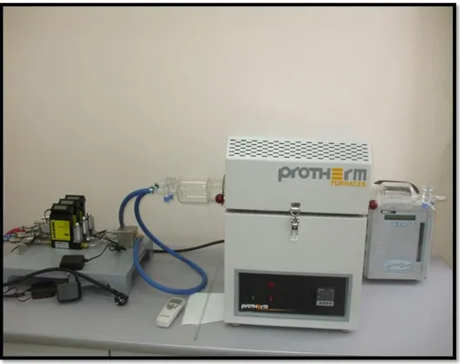
In the study, an n-Si wafer with (100) orientation and 1-10 cm resistivity is used. The wafer firstly degreased by boiling in trichloroethylene and cleaned by ultrasonically vibrating in acetone and methanol for 5 min. After each step, the wafer was washed with deionized water. After cleaning procedures, the wafer is dried under nitrogen ambient. The n-Si semiconductor was put into the vacuum chamber. Au metal was evaporated at 10-6 Torr and n-Si/Au structure was annealed under nitrogen ambient for 3 min at 570 C to make high quality ohmic contact. The annealing furnace is shown in Fig 3.6.
3.MATERIALS AND METHODS
20 3.4.1. Deposition of ZrO2 thin films
ZrO2 thin film was growth on n-Si semiconductor and quartz by reactive sputtering technique using Nanovak NVTS 400 vacuum system. Zr metal was used as target and O2 was used as reactive gas. Firstly, pressure of the vacuum system was decreased at 10-6 Torr. Argon gas was send to system and the pressure was increased to 20 mTorr. The flow of the Argon gas was about 4 ccm. 80 W power was applied to high purity Zr target and 0,4 ccm oxygen was send to vacuum system to make reactive sputtering process. This process continued 10 minutes. To increase crystallianity, ZrO2 thin film was annealed at 500 C for 30 minutes in air ambient.
MASOUD GIYATHADDIN OBAID
21
3.4.2. Formation of front contact and measurements
Au metal was evaporated to obtain front contact. The circular diameters of the Ag contacts was about 1.5 mm. To make circular front contacts a shadow mask is used. The schematic diagram of Au/ZrO2/n-Si MIS is given in Fig. 3.8.
Figure 3.8. The cross section illustratioon of Au/ZrO2/n-Si MIS diode
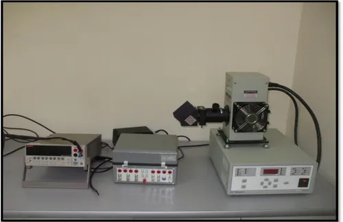
Electrical and photoelectrical characteristics of Au/ZrO2/n-Si MIS structure were analyzed using its current-voltage (I-V) and capacitance-voltage (C-V)measurements by the help of Keitley 2400 sourcemeter and Agilent 4294 A impedance analyzer at room temperature in dark, respectively. To see the effect of the light on the photoelectrical
Figure 3.9a. Current-voltage measurement system with Keithley 2400 sourcemeter and Oriel solar simulator
3.MATERIALS AND METHODS
22
Figure 3.9b. Capacitance-voltage measurement system with Agilent 4294 A Impedance analyzer
properties of the device an Oriel 9600 solar simulator was used. Current-voltage (I-V) measurements were repeated under solar simulator between 40-100 mW/cm2 with 20 mW/cm2 intervals. The current-voltage and capacitance voltage measurement systems are given in Figure 3.9.
Optical properties of the thin film on quartz was analyzed using Shimadzu 3600 uv-vis-nir spectrophometer. The system is presented in Figure 10.
MASOUD GIYATHADDIN OBAID
23 4. Findings and Discussion
4.1. Introduction
In this chapter, the experimental results of the study will be given. Firstly optical properties of the ZrO2 thin film on quartz will be analyzed. After that, electrical properties of Au/ZrO2/n-Si MIS device will be examined. Finally, the effect of light intensity on photoelectrical parameters of the diode will be studied.
4.2. Optical properties of ZrO2 thin film on quartz
UV-Vis spectra were used to determine the optical properties of the reactively sputtered ZrO2 thin film. The film was deposited quartz and its absorbance and transmittance properties were determined. Fig. 4.1 shows absorbance vs. wavelength plot of the film. As seen from the figure, the absorbance value of the film decreases sharply till 236 nm and the film has peaks at 250 and 663 nm.
Figure 4.1. Absorbance vs. wavelength plot of ZrO2 thin film on quartz
4.FINDINGS AND DISCUSSION
24
The optical band gaps (Eg) of the ZrO2 can be calculated through the equation
hvB(hvEg)m 4.1
where α is the absorption coefficient, B is a constant, h is the Plank constant, m is ½ for direct band gap and 2 for indirect band gap. ZrO2 has direct band gap. Therefore, the direct band gap of reactive sputtered ZrO2 thin film was determined by using absorption vs. wavelength data with the help of equation 4.1 using (Ahv)2–hv plot. Figure 4.2 shows the (Ahv)2–hv thin film. The Eg of the ZrO2 thin film was determined as 5.7 eV by extrapolating the straight line of the graph to intercept the photon energy. Up to now, band gap of ZrO2 thin films obtained using various methods were calculated between 5-8 eV.
MASOUD GIYATHADDIN OBAID
25
4.3. Current-voltage properties of Au/ZrO2/n-Si MIS diode
Current-voltage measurements of Au/ZrO2/n-Si MIS diode showed that the device had an excellent rectification. When the series résistance of a diode is taken into account, the relationship between current and voltage is given as (Rhoderick and Williams 1988) nkT IR V q I I exp ( s) 0 4.2
where, q is the electron charge, V is the applied voltage, RS is the series resistance, n is dimensionless ideality factor, k is the Boltzmann constant, T is the absolute temperature and I0 is the saturation current which can be written
kT qΦ T AA I b exp 2 * 0 4.3
Figure 4.3. lnI-V plots of Au/ZrO2/n-Si MIS diode in dark and various illumination conditions
4.FINDINGS AND DISCUSSION
26
Where A is the diode area, A* Richardson constant, b is the barrier height. The ideality factor of a diode can be calculated from the slope of the linear region of the InI-V plot of the diode using the equation
) ln(I d dV kT q n 4.4
The lnI-V plot of Au/ZrO2/n-Si structure measured at 300 K in dark and under various illuminations are given in Figure 4.3. The ideality factor at 300 K calculated as 5.094. The idality factor of for an ideal diode is should be unity. The deviation from 1 shows non-ideal diode behavior. This deviation can be because of the effects of native insulator layer on n-Si surface, interface states and the effect of series resistance. The electrical parameters of the Au/ZrO2/n-Si diode are given in table 4.1.
The barrier height of the junction can be calculated using I0 value obtained from interception of InI-V plot to I axis by the help of the equation
0 2 * ln I T AA q kT b 4.5 The barrier height of the device was calculated using saturation current value by the help of the equation as 0.808 eV. Kilicoglu and Asubay calculated the ideality factor and barrier height values of Au/n-Si MS contact as 1.04 and 0.742 eV (Kılıçoğlu and Asubay 2005). The results showed that the SiO2 interlayer have a strong effect on electrical parameters of Au/n-Si MS contact. Kilicoglu and Asubay fabricated Au/n-Si Schottky barrier diode with and without native oxide layer. They formed native oxide layer on n-Si wafer by exposing the Si surface to clean room air for 10 h. They studied the effect of native insulator layer on electrical performance of Schottky diode. They calculated electronic parameters of these two diodes and compared them. The values of 1.04 and 0.742 eV for ideality factor and BH of the reference sample, respectively, and the values of 1.15 and 0.743 eV for the ideality factor and BH of Au/native oxide/n-Si, respectively, were obtained. The values of all electronic parameters of Au/native oxide/n-Si metal–insulator–semiconductor (MIS) SBDs except for the rectifying ratio have been found to be higher than values of the reference sample (MS).
MASOUD GIYATHADDIN OBAID
27
Table 4.1. Some electrical parameters of Au/ZrO2/n-Si MIS device at room temperature
lnI-V Norde C-V
n b (eV) F(V0) V0 b (eV) RS () b (eV) Nv (cm-3)
5.094 0.808 0.7485 1.427 0.96 50 0.916 2.901x10¹⁵
Current-voltage measurements of the plots presented in Figure 4.4 have deviation from linearity for high voltages. This deviation implies the effect of series resistance. The series resistance results from the contact wires or bulk resistance of the
ZrO2 and n-Si semiconductors. The series resistances of the Au/ZrO2/n-Si structure
were calculated by means of Norde functions given below as (Norde 1979)
(* )2 T AA V I q kT V V F 4.64.FINDINGS AND DISCUSSION
28
where γ is the first integer greater than ideality factor and I(V) is the current obtained from I–V measurements. The barrier height of device can be calculated using the minimum value of F vs. V plot using the equation
q kT V V F b 0 0) ( 4.7
where F(V0) is the minimum F(V) value and V0 is the corresponding voltage value. F(V)–V curve of Au/ZrO2/n-Si heterojunction structure is shown in Figure 4.5. The series resistance of the device is executed through the relation
min qI n kT RS 4.8where Imin the corresponding current value at V0.
The barrier height and the series resistance values of the heterojunction are also depicted in table 1. As it is seen from the table, the barrier height and the series resistance of the diode calculated as 0.96 eV and 50 . Güllü et al fabricated Cu/n -InP Schottky junction with organic dye (PSP) interlayer (Güllü, Aydoğan et al. 2012). An effective barrier height as high as 0.82 eV has been achieved for Cu/PSP/n-InP Schottky diodes, which have good current–voltage (I–V) characteristics. This good performance is attributed to the effect of formation of interfacial organic thin layer between Cu and n-InP. The ideality factor and barrier height for one of the Cu/PSP/n n-InP contacts is calculated 1.01 and 0.82 eV, respectively. The barrier height value of 0.82 eV calculated for one of the Cu/PSP/n-InP contacts is higher than value of 0.45 eV for Cu/n-InP conventional diode.
4.4. Photoelectrical properties of Au/ZrO2/n-Si MIS diode
Figure 4.3 shows also the current-voltage plots of Au/ZrO2/n-Si MIS diode for
various light intensities. As seen from the figure, light intensity has a strong effect on photoelectrical performance of the device. Some photoelectrical parameters including sensitivity to light at -5V (illuminated current/dark current), open circuit voltage (VOC)
and short circuit current (ISC) values are given in table 4.2. As seen from the table, all
MASOUD GIYATHADDIN OBAID
29
Table 4.2. Photoelectrical parameters of Au/ZrO2/n-Si MIS device at room temperature Light Intensity ISC (A) VOC (mV) Sensitivity to light (Times)
40 mW/cm2 2.97 326 889
60 mW/cm2 5.25 326 2687
80 mW/cm2 5.92 347 3884
100 mW/cm2 8.62 373 5241
showed that the device had photodiode characteristics which are attributable to the formation of electron–hole pairs following optical absorption. Similar results have been reported for various MIS diodes. For instance, Ocak et al fabricated a
metal/interlayer/semiconductor (Al/enzyme/p-Si) MIS device was fabricated using α-amylase enzyme as a thin biofilm interlayer (Ocak, Guven et al. 2013). They studied the photovoltaic properties of the structure under a solar simulator with AM1.5 global filter between 40 and 100 mW/cm2 illumination conditions. They reported that the Al/enzyme/p-Si had better response to light with compared to Al/p-Si MS diode.
4.5. Capacitance-voltage properties of Au/ZrO2/n-Si MIS diode
Capacitance-voltage measurements Au/ZrO2/n-Si MIS diode for various
frequencies are depicted in Figure 4.5. As it is seen from the figure, capacitance value of the structure decreased for forward bias values with the increase in frequencies. It means that at sufficiently high frequencies, charge carriers at the interface can no longer follow the AC signal. This situation showed the strong effect of interface states to capacitance of the structure. The depletion region capacitance of a diode is given
d N A s q V bi V 2 2 2 C 1 , (4.9)where Vbi is the built-in potential, εS is the dielectric constant of the semiconductor and Nd is the donor concentration. Nd was determined from the intercept of a plot of C-2 as a
function of V, and Vbi was determined from the gradient of this plot, as shown in Fig.
4.7. The barrier height and the donor concentration of the Au/ZrO2/n-Si diode were
4.FINDINGS AND DISCUSSION
30
Figure 4.5 C-V plots of Au/ZrO2/n-Si MIS diode at various frequencies
MASOUD GIYATHADDIN OBAID
31
height value of the diode is higher than the one obtained from lnI-V plot. Owing to the different nature of measurements, different barrier height values can be calculated from I-V and C-V methods. It is known that the capacitance of a diode is insensitive to potential fluctuations at the interface and C-V method averages over the whole area and measures to describe barrier height. On the other hand, the current across the interface exponentially depends on barrier height and highly sensitive to the interface state densities.
4.FINDINGS AND DISCUSSION
32
MASOUD GIYATHADDIN OBAID
33 5. Results and Suggestions
In this study, electrical and photoelectrical characterization of Au/ZrO2/n-Si MIS contact were investigated. For this porpose, ZrO2 thin film was deposited on n-Si/Au and quartz substrates by reactive sputtering of Zr metal target at room temperature. The ZrO2 thin film was annealed for an hour at 500 ⁰ C to increase the crystal quality.
UV-Vis spectra were used to determine the optical properties of the reactively sputtered ZrO2 thin film. The film was deposited quartz and its absorbance properties were determined. It was seen that the absorbance value of the film decreases sharply till 236 nm and the film has peaks at 250 and 663 nm. The direct band gap of reactive sputtered ZrO2 thin film was determined by using absorption vs. wavelength data with the help of equation 4.1 using (Ahv)2–hv plot as 5.7 eV. Therefore It was seen that reactively sputtered ZrO2 thin film had very high band gap and it can be used as insulator layer between metal and semiconductor.
Current-voltage measurements of Au/ZrO2/n-Si MIS diode showed that the device had an excellent rectification. The ideality factor at 300 K calculated as 5.094. The barrier height of the device was calculated using saturation current value by the help of the equation as 0.808 eV. The ideality factor greater than unity for Au/ZrO2/n-Si diode was attributed the effects of native insulator layer on n-Si surface, interface states and the effect of series resistance. Furthermore, the barrier height of Au/ZrO2/n-Si device was higher than the barrier height of Au/n-Si MS contact (0.742 eV) reported by Kilicoglu and Asubay. The barrier height and the series resistance values of the heterojunction are also calculated using Norde method as 0.96 eV and 50 .
The current-voltage plots of Au/ZrO2/n-Si MIS diode for various light intensities
were drawn to see the effect of light on photoelectrical parameters of the device. Some photoelectrical parameters including sensitivity to light at -5V (illuminated current/dark current), open circuit voltage (VOC) and short circuit current (ISC) values are given in
table 4.2. As seen from the table, all photoelectrical parameters increase with the increase in light intensity. This property showed that the device had photodiode characteristics which are attributable to the formation of electron–hole pairs following optical absorption.
Finally, capacitance-voltage measurements Au/ZrO2/n-Si MIS diode for various
5. RESULTS AND SUGGESTIONS
34
for forward bias values with the increase in frequencies. It means that at sufficiently high frequencies, charge carriers at the interface can no longer follow the AC signal. This situation showed the strong effect of interface states to capacitance of the structure. The barrier height and the donor concentration of the Au/ZrO2/n-Si diode were executed
as 0.916 eV and 2.901x1015 cm-1, respectively. The barrier height value of the diode was higher than the one obtained from lnI-V plot. This difference was attributed the
MASOUD GIYATHADDIN OBAID
35 6. References
Chang, H. S., S. Jeon, et al. (2002). "Excellent thermal stability of Al2O3/ZrO2/Al2O3 stack structure for metal–oxide–semiconductor gate dielectrics application." Applied Physics Letters 80(18): 3385-3387.
Cheung, S. and N. Cheung (1986). "Extraction of Schottky diode parameters from forward current‐voltage characteristics." Applied Physics Letters 49(2): 85-87. Cowley, A. and S. Sze (1965). "Surface states and barrier height of
metal‐semiconductor systems." Journal of Applied Physics 36(10): 3212-3220. Evangelou, E., C. Wiemer, et al. (2003). "Electrical and structural characteristics of
yttrium oxide films deposited by rf-magnetron sputtering on n-Si." Journal of Applied Physics 94(1): 318-325.
Gökçen, M., Ş. Altındal, et al. (2011). "Forward and reverse bias current–voltage characteristics of Au/n-Si Schottky barrier diodes with and without SnO 2 insulator layer." Physica B: Condensed Matter 406(21): 4119-4123.
Güllü, Ö., Ş. Aydoğan, et al. (2012). "High barrier Schottky diode with organic interlayer." Solid State Communications 152(5): 381-385.
Hudait, M. K. and S. Krupanidhi (2000). "Effects of thin oxide in metal–semiconductor and metal–insulator–semiconductor epi-GaAs Schottky diodes." Solid-State Electronics 44(6): 1089-1097.
Kılıçoğlu, T. and S. Asubay (2005). "The effect of native oxide layer on some electronic parameters of Au/n-Si/Au–Sb Schottky barrier diodes." Physica B: Condensed Matter 368(1): 58-63.
Kınacı, B., S. Ş. Çetin, et al. (2012). "The temperature dependent analysis of Au/TiO 2 (rutile)/n-Si (MIS) SBDs using current–voltage–temperature (I–V–T) characteristics." Materials Science in Semiconductor Processing 15(5): 531-535. Mönch, W. (1999). "Barrier heights of real Schottky contacts explained by metal-induced gap states and lateral inhomogeneities." Journal of Vacuum Science & Technology B 17(4): 1867-1876.
Mönch, W. (2013). Semiconductor surfaces and interfaces, Springer Science & Business Media.
Norde, H. (1979). "A modified forward I‐V plot for Schottky diodes with high series resistance." Journal of Applied Physics 50(7): 5052-5053.
Ocak, Y., M. Kulakci, et al. (2009). "Current–voltage and capacitance–voltage characteristics of a Sn/Methylene Blue/p-Si Schottky diode." Synthetic Metals 159(15): 1603-1607.
6. REFERENCES
36
Ocak, Y. S., R. G. Guven, et al. (2013). "Barrier height enhancement of metal/semiconductor contact by an enzyme biofilm interlayer." Philosophical Magazine 93(17): 2172-2181.
Oh, H. G., K. S. Kim, et al. (2013). "Low Frequency Noise Characteristics on Al/Nb2O5/p-type Schottky Diode Fabricated by Pulsed DC Magnetron Sputtering." Molecular Crystals and Liquid Crystals 586(1): 168-178.
Rhoderick, E. H. and R. Williams (1988). Metal-semiconductor contacts, Clarendon Press Oxford.
Schottky, W., R. Stormer, et al. (1931). "Rectifying Action at the Boundary between Cuprous Oxide and Applied Metal Electrodes." Z. Hoch Frequentztechnik 37: 162.
Sze, S. and K. N. Kwok (2007). Physics of semiconductor devices 3rd Edition, Wiley Online Library.
MASOUD GIYATHADDIN OBAID
37 Curriculum Vitae
Name Masoud Giyathaddin Obaid Address Shorash Quarter Duhok city Telephone 00964(0750)4834973
Mail [email protected] Nationality Iraq \ Kurdish
Date of birth 1 March 1980 Marital status Married Education / Qualifications
I have the following certifications
1) In 1995 – 1998, I graduated from Kawa preparatory school in Duhok city.
2) In 1998 – 2002, I graduated from Duhok University: College Of Science / physics Department with a B.SC. Degree In physics
3) In 2003 -2008, I graduated from Duhok University: College of Arts / English Department with a B.A. Degree in English Arts
4) In 2011 – 2012, I graduated from Duhok University: Faculty of Engineering/ school of planning with a High Diploma Degree in Planning,
5) In 1/10/2013 I joined to the Dicle University in Turkey for studying M.Sc. Degree in physics.
Employments to date
Within the period of 2002 – and upto now I work as a teacher of physics and English in Duhok city, now I am a teacher in College of Duhok for Gifted students in Duhok city, a teacher of Physics.
Skills Computer literate: I am familiar with a number of design programs, PowerPoint, Microsoft office programs (Word, Excel, and Access).
Languages: I can speak three languages English, Arabic and Kurdish. Interests Swimming, Chessboard, Reading