Band Offsets, Optical Conduction, Photoelectric and Dielectric Dispersion in InSe/Sb
2Te
3Heterojunctions
Latifah Hamad Khalid Alfhaida, A. F. Qasrawib,c*, Sabah E. AlGarnid
aUniversity of Ha’il, Collage of Science, Department of Physics, Ha’il, Saudi Arabia bArab American University, Department of Physics, Jenin, Palestine
cIstinye University, Department of Electrical and Electronics Engineering, 34010, Istanbul, Turkey dUniversity of Jeddah, Faculty of Science, Department of Physics, Jeddah, Saudi Arabia
Received: December 18, 2020; Revised: April 07, 2021; Accepted: April 24, 2021
InSe based heterojunction devices gain importance in optoelectronic applications in NIR range as multipurpose sensors. For this reason, InSe/Sb2Te3 heterojunctions are constructed as NIR sensors by the thermal evaporation technique. The structural, optical, dielectric and photoelectric properties of InSe/Sb2Te3 heterojunctions are explored by X-ray diffraction and ultraviolet-visible light spectrophotometry techniques. The structural analyses revealed the preferred growth of polycrystalline hexagonal Sb2Te3 onto amorphous InSe as a major phase. Optically, the coating of Sb2Te3 onto InSe enhanced the light absorbability of InSe by more than 18 times, redshifts the energy band gap, increased the dielectric constant by ~5 times and increased the optical conductivity by 35 times in the NIR range of light. A conduction and valance band offsets of 0.40 and 0.68 eV are determined for the InSe/Sb2Te3 heterojunction devices. In addition, the Drude-Lorentz fittings of the optical conductivity indicated a remarkable increase in the plasmon frequency values upon depositing of Sb2Te3 onto InSe. The illumination intensity and time dependent photocurrent measurements resulted in an enhancement in the photocurrent values by one order of magnitude. The response time of the devices is sufficiently short to nominate the InSe/Sb2Te3 heterojunction devices as fast responding NIR sensors suitable for optoelectronic applications.
Keywords: InSe/Sb2Te3, dielectric, band offset, Drude-Lorentz model.
1. Introduction
One of the famous research sectors which are popular in the current century is the design of new classes of semiconducting materials that suits many optoelectronic applications. These semiconductor groups include organic/ inorganic1, metal-(double) oxides2-4 layers and mixed metal-oxide nanoparticles5. Organic Cr-Co mixed crystals is mentioned suitable for fabrication of micro-nano devices5. In addition, Cr–Ni OSC complexes are observed to exhibit energy band gaps of ~1.87 eV which nominates it for use in visible light communications as signal receivers3. Moreover, carboxymethyl cellulose zinc thin films which were fabricated using the sol–gel technique and widely tested are found to be ideal materials for use in producing photosensors and solar cells6,7. As nanoparticles, Co-Al oxides are reported promising alternative materials for improving the power conversion efficiency of solar cells and for obtaining clean and renewable energy4.
Another interesting material is antimony telluride in thin films forms which attracted the attention of research society owing to their wide range of applications. They can exhibit different characteristics that depend on the substrates they grow onto. As for examples, Sb2Te3 films coated onto Bi2Te3 are observed to behave as a planer
thermoelectric generator8. n-Bi
2Te3/p-Sb2Te3 heterojunctions which are prepared onto Kapton substrates generated open circuit voltage of 0.21 V and output power of 3.3mW/cm2. As another example, Sb2Te3 films are employed as templates to enable fast memory switching of phase change materials like GeSb2Te49. Sb
2Te3 coated onto Ge-Sb-Te substrates is nominated for as promising heterojunctions for enhancing the speed of response of phase-memory change devices9. In addition, Sb2Te3 thin films which are deposited onto CdTe based solar cells, improved the solar cell efficiency up to 8.01%10. Moreover, the vertically stacked layers of Sb2Te3 and MoS2 formed heterojunctions that are suitable for high performance optoelectronic applications11. The current rectification ratio of this device reached 106. It also displayed excellent photovoltaic properties. Furthermore, antimony telluride films coated onto Si substrates displayed photodetector characteristics presented by a self- powered fast and broad band photodetection. The response time of this device was less than 40 ms12.
In one of our recent works13-15, we have also shown that a thin layer (20 nm) of Sb2Te3 can significantly improve the performance of CdS and force it exhibiting negative capacitance effect in the frequency range of 260-1800 MHz. The CdS/Sb2Te3 heterojunction devices were usable as a wide range low pass filters displaying ideal voltage standing wave ratios. In the light of the above mentioned inventions, *e-mail: [email protected]
here in this work, we are motivated to construct a new class of heterojunction devices that get benefit from Sb2Te3. Namely, Sb2Te3 films of thicknesses of 300 nm are coated onto InSe substrates of thicknesses of 1.0 µm. The formed
InSe/Sb2Te3 heterojunctions are structurally, optically and photo-electrically characterized. The characterizations include the crystallization and growth nature, the light transmittance, reflectance and absorbance, identification of energy band offsets and energy band gaps as well. The dielectric dispersion and optical conductivity dynamics at the InSe/Sb2Te3 interfaces are also included. In addition, the light intensity and time dependencies of the photocurrent are also considered.
2. Experimental Details
Indium selenide-antimony telluride heterojunction devices are prepared by the thermal evaporation technique using NORM VCM -600 thermal evaporator. The vacuum pressure was kept at 10-5 mbar. The InSe films were coated onto chemically and ultrasonically cleaned glass substrates. The grown indium selenide thin films were of thicknesses of 1.0 µm. The grown glass/InSe films were masked and covered with Sb2Te3 thin films. The thickness of Sb2Te3 thin films was 300 nm. This thickness was selected to allow minimum light transmittance and increase the reflectance. The high reflectance values leads to higher values of dielectric constants. The resulting InSe/Sb2Te3 films were coated with Ag pads of areas of 3.14×10 cm−2 2. The geometrical
design of the device with Ag pads is shown in the inset of Figure 1. The thickness of the films was measured with the help of Inficon STM-2 thickness monitors attached to the evaporator. The thickness was confirmed with surface roughness tester-profilometer (Model SOLID TR-200 plus). The structural characterizations were carried out with the help of MINIFLEX 600 X-ray diffraction unit. The optical transmittance and reflectance spectra were measured with the help of Thermoscientific evolution 350 spectrophotometer. The spectrophotometer is equipped with VEE MAX II reflectometer. The electrical measurements were done with the help of Keithley current-voltage characteristics system. The system is composed of Keithley 230 voltage source and Keithley 6485 Picoammeter. The light was irradiated from a tungsten lamp and daylight light emitting diode. The light intensity were measured with the help of a wide range lux meter.
3. Results and Discussion
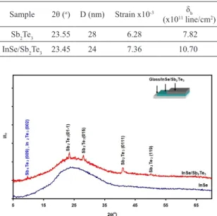
The geometrical design and X-ray diffraction patterns for the InSe/Sb2Te3 thin films which are prepared by a vacuum evaporation technique are shown in Figure 1. In accordance with the figure, no sharp diffraction patterns are observed for InSe films. The broaden XRD patterns of InSe reveal an amorphous nature of structure. On the other hand, Sb2Te3 thin films which are coated onto glass substrates displayed intensive peaks at various diffraction angles. The observed sharp peaks were compared to the standard PDF cards of Sb2Te3 (JCPDS card No. 15-0874), Sb4Te3 (crystallography open database COD: 7113353)), InSe (card No.: 34-1431), Te ( JCPDS Card No. 36-1452), Sb (JCPDS card no. 85-1324) and In2Te3 (JCPDS card: 33-1488) . The formed crystalline
phases of the InSe/Sb2Te3 interface are mostly assigned to the hexagonal (a b 4 264= = . Å, c 30 485= . , Åγ=120o) Sb2Te316,17. One minor peak detected at 2θ=9 95. o was related to the
hexagonal (a b= =4.275 Å, c =83.564 Å, γ =120o ) phase of
Sb4Te3. This peak is also in good agreement with the reflection peaks of the cubic (a b c 18 48= = = . Å) In2Te3.
On the other hand, as appears in Table 1, the calculated structural parameters presented by the crystallite size ( .
( )
; :cos 0 94
D=β λ βθ maximum peak broadening18), microstrain
(∈ β= / (4tan( )θ 18), and defect density ( /( )
b 15 bD δ = ∈ 18) are calculated for the peaks oriented along the (01-1) direction. While the crystallite sizes decreased from 28 to 24 nm, ∈ ,
and δb increase from 6.28×10⁻³, and 7.82×10 line cm11 / 2 to
7.36×10⁻³, and 10.70×10 lines cm11 / 2, respectively when Sb2Te3 was coated onto InSe substrates. The decrease in the grain size may be assigned to the increased surface roughness upon coating of Sb2Te3 onto InSe substrates18,19. As previously mentioned, the increased/decreased in average crystallite size was confirmed by reduced/enhanced dislocation density and micro strain and is assigned to the large difference between the surface energy of the differently oriented planes20.
In general, Sb2Te3 crystals are similar in structure to Bi2Se316,17
. In these materials, the hexagonal unit cells are formed from quintuple layers oriented along the (0001) direction of the hexagonal unit cell. Each layer is composed of five covalently bonded Te-Sb-Te-Sb-Te atomic sheets. While the interactions between two adjacent quintuple layers are predominated by the weak van der Waals forces, interactions between the atomic sheets which exists within a quintuple layer is strong. Hence, the cleaving planes are centered between the quintuple layers and should always terminate with Te atomic layers. In Sb4Te3, similar to the structure of (Bi2Se3)m(Bi2) two extra Sb layers are added to the sequence of stacking order owing to richness of Sb that results from breaking the weaker bonds in a neighboring quintuple
Table 1. The structural parameters for antimony telluride grown
onto glass and InSe substrates.
Sample 2θ (o) D (nm) Strain x10-3 δb
(x1011 line/cm2)
Sb2Te3 23.55 28 6.28 7.82
InSe/Sb2Te3 23.45 24 7.36 10.70
Figure 1. The X-ray diffraction patterns for InSe and InSe/Sb2Te3
layers16. Owing to the close values of bond lengths of Sb-Te (303 pm17) and In-Se (296 pm21), interaction between In and Te to form indium telluride is probable. However, since InSe is of amorphous nature, its surface is expected to have large amount of In-Se broken bonds. The capturing of indium ion to a weakly bonded tellurium ion (bond length of In-Te is 272 pm22) leave one Sb ion not bonded. Such variations in the bonding mechanisms could account for the changes in the covalently bonded layers resulting in the appearance of Sb4Te3 or appearance of In2Te3 as well.
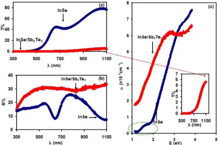
Figure 2a and b illustrate the transmittance (T) and reflectance (R) spectra for InSe films before and after coating with Sb2Te3. It is clear from the figure that the transmittance remarkably decreased by more than fourteen times upon coating of InSe with Sb2Te3. The local maxima which are observed at 656 nm in the Tspectra of InSe disappeared. On the other hand, the reflection spectra of InSe which are displayed in Figure 2b exhibit one absolute and one local minima at an incident light wavelengths (λ) of 540 and 780 nm, respectively. Coating of InSe with antimony telluride increased the reflectance of InSe, changed the shape of variations of the R−λ dependencies and forced cancellation of the reflectance peaks. The total effects of the Sb2Te3 coatings on the optical properties of InSe are evident from the absorption coefficient (α) spectra. The absorption coefficient for stacked layers of total thickness d is calculated from the relation23,24,
(
)
(
)
(
)
(
)
(
)
/ / 2 3 2 3glass InSe InSe Sb Te glass InSe InSe Sb Te
1 R 1 R 1 R exp d T 1 R R R exp 3 d α α − − − − = − − (1)
Equation 1 takes the form,
(
)
(
) (
)
(
)
glass InSe glass InSe 1 R 1 R exp d T 1 R R exp 2 d α α − − − = − − (2)when used for glass/InSe films. α spectra for InSe and InSe/Sb2Te3 films are shown in Figure 2c.
As seen from the figure, the absorption coefficient values for InSe follow a sharp trend of variation in two easily distinguishable high (3.30-1.90 eV) and low (1.70-1.30 eV) energy regions. α-spectra of InSe/Sb2Te3 displays only one
sharp trend of variation in the range of 2.73-1.31 eV. It is also clear from Figure 2c that the coating of Sb2Te3 onto InSe films redshifts the absorption coefficient spectra and increased α values. As for examples, the absorption coefficient
of InSe which exhibits value of 1.0×10 cm4 −1 at 2.0 eV
reaches 4.45×10 cm4 −1 at the same incident photon energy.
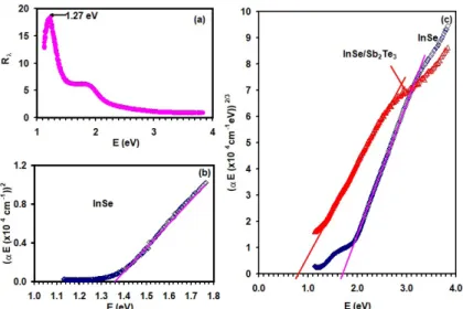
The calculated light absorbability, InSe Sb Te/ 2 3
InSe
Rλ
α α
= is shown in Figure 3a. Rλ spectra exhibit values larger than one for
all incident photon energy values in the range of 3.0-1.1 eV. It means that coating of Sb2Te3 onto InSe highly enhanced the light absorbability of InSe. The smaller the energy value is, the larger the light absorbability. The highest recordable
Rλ values is 18.5 at 1.27 eV. The enhanced light absorbability
makes the InSe more suitable for optoelectronic applications. The increase in the absorption coefficient and light absorbability can be assigned to the increase in the volume of the absorbing material upon InSe/Sb2Te3 interfacing25. It could also be assigned to the higher efficiency of energy transfers that is reached by suppressing the unbonded or dangling ions at the InSe surface26. The enhanced absorption characteristics may have resulted from the formation of the clusters of Sb4Te3 and In2Te3 at the ultrathin interface. These two minor phases were observed in the XRD patterns (Figure 1).
To reveal clearer idea about the changes in the optical transitions as a result of stacking of Sb2Te3 with InSe, Tauc’s equation,
( )
αE =(
E E− g)
n (3)was employed. Theoretically n is equal to 2, 1/2, 3 or 3/2 for the indirect allowed ( IA
g
E ), direct allowed (EgdA), indirect
forbidden ( IF g
E ) and direct forbidden ( dF g
E ) transitions, respectively3,27.The decision about the favorable transition type is taken in accordance with the equation that linearly
fits the widest range of data. As seen from Figures 2b and c, for InSe films, the most appropriate fitting in the low (1.70-1.30 eV) and high (3.30-1.90 eV) absorption regions are the
( )
2(
)
g E E E α = − and( )
2 3/(
)
g E E E α = − , respectively. Two types of optical transitions are presented in InSe. The respective E −axis crossings of the figures reveal the energy band gap values of dA .g
E =1 36 eV and dF .
g
E =1 70e
V. The coating of InSe with Sb2Te3 resulted in one energy band gap type (direct forbidden energy band gap) of value of dF .
g
E =0 80 eV. A large redshift by ~ 0.90 eV is observed
as a result of interfacing of InSe with Sb2Te3. The energy band gap values of InSe being 1.36 eV and 1.70 eV were previously observed. Values of 1.77 eV were previously observed for In2Se3 films23 and values of dA
g
E = 1.36 eV are reported for indium monoselenide films prepared by the thermal evaporation28 and laser sublimation and chemical deposition techniques29. The value of the energy band gap for InSe/Sb2Te3 bilayers being 0.90 eV mostly arises from interactions between indium and tellurium at the ultrathin interface. As we suggested through the XRD analyses the bonding between indium and tellurium forced formation of Sb4Te3 or In2Te3 as minor phase in the structure of Sb2Te3. Interactions between In and Te forms In2Te3. The energy band gap of In2Te3 is reported to exhibit values in the range of 0.80-0.99 eV30,31. The bonding energy of In–Te being 218.0 kJ/mol is much larger than that of In–Sb (151.9 kJ/mol32), of Sb-Se (183.89 kJ/mol33) and of In-Se (48.2 kJ/mol34). The larger the bonding energy is, the stronger the interaction with the surrounding atoms, the more difficult the vacancy formation35. Other studies which take into account the linear optical properties and nonlinear absorption behaviors of Sb2Se3 and Sb2Te3 have shown that the metallic character of Sb2Te3 is much stronger than that of Sb2Se336. The attenuation in the optical parameters in these materials is assigned to the pronounced metal character36,37. Replacement of Se by Te in Sb2Se3 redshifted the energy band gap from 1.20 eV to 0.30 eV38.
The compositional variations in InSe and Sb2Te3 could also play main role in determining the values of the energy
band gaps. Mn, Fe and Co doped ZnO films displayed wide variety in the energy band gap value depending on the doping agent and content39,40. For InSe variation of atomic composition of In was sufficient to change the energy band gap from 1.88 eV to 1.12 eV as indium content increases41.
In accordance with the energy band theory, InSe and Sb2Te3 exhibit electron affinities (qχ) 4.55 and 4.15 eV, respectively. These values lead to a conduction band offset (∆Ec) of 0.40 eV. Since the energy band gap of Sb2Te3 is 0.28 eV12, the energy band gap difference is 1.42/1.08 eV. As a result, the valence band offset is 1.02 eV/0.68 eV. The most preferable value is 0.68 eV as it should be between the two direct allowed transitions energy band gaps of InSe and Sb2Te3. The value of ∆Ev is sufficiently large to
allow using InSe/Sb2Te3 stacked layers in optoelectronic applications and thin film transistor technology. As mentioned, the larger the valence band offset at the interface, the less band bending is required to achieve good tunneling contacts42.
Figure 4a and b represents the respective effects of Sb2Te3 coatings onto InSe on the real (εr) part of the dielectric and
on the optical conductivity (σ( )w w ; is angular frequency) spectra. Both of the εr and σ
( )
w are calculated from themeasured reflectance and absorption coefficient spectra with the help of Fresnel’s equation21,43,
( ) ( ) 2 2 eff 2 2 eff 1 K R 1 K ε ε − + = + + (4)
Here, εeff is the effective dielectric constant,
, 2
r eff
K=αλ ε ε4π = −K and σ( )w =εimw 4/( )π =2w εeffK 4/( )π 43. As Figure 4a shows, coating of InSe with Sb2Te3 highly enhanced the values of dielectric constant and changes its shape of variation. While the εr spectra of InSe display
two peaks centered at 2.31 and 1.63 eV, the spectra of InSe/Sb2Te3 display one peak at 2.31 eV. In the spectral region of 1.63-1.14 eV, the dielectric constant of InSe
Figure 3. (a) the light absorbability and the Tauc’s equation fittings for (b) InSe in the low absorption region and (c) for InSe and InSe/
decreases and that of InSe/Sb2Te3 increases with decreasing energy of incident photons. The ratio of the dielectric constants ( r InSe Sb Te/ 2 3 r InSe Rε ε ε − −
= ) before and after the coating
of Sb2Te3 onto InSe is also illustrated in Figure 4a.
Rε increases with decreasing incident photon energy
exhibiting a peak at 1.96 eV. In all the studied spectral range, the dielectric constant values are enhanced by more than one time. The dielectric constant increases by 4.7 times at 1.14 eV. As we concluded from Tauc’s equation analyses, the critical energy being 1.63 eV (comparable with dF .
g
E =1 70eV ) at which the dielectric
constant of InSe exhibits a maxima is attributed to the direct forbidden transitions from the valence to the conduction band of InSe. The critical energy value being 2.31 eV is close to the previously observed at 2.40 eV. This peak was assigned to the electronic transitions between the top of the valence band which is composed of px,y orbitals
along (110) direction in k-space and the bottom of the conduction band formed from pz-like orbitals along (001) direction in k-space44.
It is also clear from Figure 4b that a significant improvement in the optical conductivity values of InSe is achieved via Sb2Te3 coating. In accordance with the figure, the optical conductivity ratios (Rσ =σInSe Sb Te/ 2 3/σInSe ) is always larger than
one. The lower the incident photon energy, the larger the value of Rσ. The enhancement in the optical conductivity reach more
than 35 times at 1.19 eV. The enhanced optical conductivity is mentioned to be beneficial in designing photonic and optoelectronic devices such as solar cells and light-emitters45. It is also regarded as promising features for use in visible light communications as signal receivers46,47.
As a confirmation procedure for the usability of the InSe/Sb2Te3 as optoelectronic devices, we first compute the optical conductivity parameters by using the Drude-Lorentz
model for optical conduction46,47. In this model the optical conductivity is given by the equation,
( )
(
)
2 2 n pei i 2 2 2 2 2 i 1 ei w w w 4 w w w γ σ π γ = = − + ∑ (5)In the above equation, the electron-plasmon reduced frequency is we. It represents the reduced resonant frequency
that takes into account the effects of the interband transitions on the optical conductivity function. γ τ= −1 is the damping constant which is related to the inverse of the scattering time (τ) and the plasma frequency (wpe) is given by the relation,
/ * 2 pe
w = 4 ne mπ (6)
Here n is the free carrier density, m* is effective mass of charge carriers. From these parameters, the drift mobility can also be estimated using the relation, µ=e mτ/ *. The computed
conductivities that best fit the experimental data are shown by solid black circles in Figure 4b. While computing the optical conductivities the effective masses of electrons in InSe and of holes in Sb2Te3 were taken as 0 156m. o16 and as 0 590m. o48,
respectively. The effective mass * / 2 3
InSe Sb Te
m is calculated from the relation, *
(
*) (
*)
/ 2 3 2 3 1 1 1 InSe Sb Te Sb Te InSe m = m − + m − − ].
The value of m*InSe Sb Te/ 2 3is found to be 0 123m. o.
The computed optical conductivity parameters are displayed in Table 2. As the table shows, for the first three oscillators (n 1 2 3= , , ), while the scattering time at femtosecond
level is shortened and the drift mobility is decreased, the free carrier density and plasmon frequency are highly increased upon interfacing of InSe with Sb2Te3. The plasmon frequency increased from 0.50 GHz to 2.9 GHz at reduced oscillator angular frequency of 2.0×10 rad s15 / (1.31 eV). It also
increases from 1.6 GHz to 8.1 at . . 15 / e2
w =3 0 3 5 10 rad s− ×
Figure 4. (a) the real part of the dielectric constant spectra and (b) the optical conductivity spectra for InSe and InSe/Sb2Te3 heterojunctions.
(1.96-2.30 eV). The values of the plasmon frequency are high enough to nominate the constructed heterojunction device as microwave resonators. Since larger plasmon frequencies are reachable, it is possible to suggest that interfacing of InSe with Sb2Te3 is more effective for production microwave cavities than InSe/Ge/InSe47 or than InSe/CdSe heterojunctions21. The shorter scattering time means the electronic friction has increased as a result of heterojunction formation. This is expected because electronic motion finds energy barriers at the depletion region of the n −InSe/p −Sb2Te3 interfaces. It is also worth reminding that the valence band offsets is large enough to control electron –hole recombination at the interface. In addition, the band bending mechanisms at the interface requires re-alignment of the Fermi level. As the energy of Fermi level increases more higher-order plasmonic levels can be expected49.
It is interesting to remind that the refractive index is related to the effective dielectric constant through the relation, εeff =n2. When the refractive index, n( )λ , is
analyzed using the single-effective-oscillator models50 using the relation, ( ) 2 d o 2 2 o E E n E 1 E E = + − (7)
with Ed being the dispersion energy of the oscillator whose
energy Eo, the plot of
(
)
1 2n −1− as function of E2 allows the determination of the oscillator parameters, by fitting a linear function using Equation 7. The fitting result in the equation,
o 2 d o d E E 1 E E E
n −1= − =1.60-0.84 E. This equation revealed value
of Ed=0 92eV. and Eo=1 39eV. . The oscillator energy being
1.38 eV is very close to the one we determined as 1.31 eV (Table 2) for InSe in the IR range from Drude-Lorentz approaches50. For InSe/Sb
2Te3, the slope of the fitting is positive indicating that using the single oscillator model is not valid for this heterojunction. However, with linearly summed oscillators, the optimization of optical conductivity parameters is possible.
As a second confirmation procedure of the applicability of the proposed InSe/Sb2Te3 heterojunctions as visible light communication receivers, two Ag pads of areas of ~4.0×10⁻² cm2 were located at 0.4 cm from each other. As shown in the inset of Figure 1, one of the pads is on the surface of InSe and the other is on the surface of Sb2Te3. The light was irradiated from a daylight light emitting diode onto the back side of the heterojunction devices to record the time varying signals. It was also back irradiated with
Table 2. Optical conductivity parameters for InSe and InSe/Sb2Te3 interfaces.
n (cm−3) InSe InSe/Sb2Te3 1 2 3 4 1 2 3 4 ( )fs τ 0.9 0.5 0.5 0.4 0.4 0.3 0.3 0.3
(
×1018cm−3)
n 0.1 1.2 18.0 36.0 3.0 23.0 28.0 28.0(
×11015Rad s/)
e w 2.0 3.0 4.5 5.8 2.0 3.5 4.0 5.8 = o e E w (eV) 1.31 1.97 2.95 3.80 1.31 2.29 2.62 3.80(
GHz)
p w 0.5 1.6 6.4 9.0 2.9 8.1 9.0 9.0(
cm Vs2/)
µ 10.14 5.64 5.64 4.51 5.72 4.29 4.29 3.57Figure 5. (a) the photocurrent-illumination intensity dependence and (b) the time dependent illuminated current for the planner Ag/InSe/
a tungsten lamp to study the light illumination intensity (
P) dependence of photocurrent (Iph). The resulting Iph−P variation is shown in Figure 5a. The figure illustrates a response of the photocurrent by more than one order of magnitude to an incident light signal. The Iph−P variation can be presented by the relation, g
ph
I ∝P . The logarithmic
plot of Iph−P dependence follows two slopes that reveal
g values of 0.70 and 0.39 in the low and high illumination
intensity regions, respectively. These two numerical values indicate that the recombination mechanism in the InSe/ Sb2Te3 heterojunctions is strongly affected by the exponential trap distributions51. Surface trap states are generated by defects and vacancies. Trapping states attenuate the position of the Fermi levels in the dark. Under illumination the quazi Fermi levels are also shifted leading to the sublinear relation (g 1 0< . ) between Iph and P. Cases where g 0 5~ . indicates that the density of charge carries trapped below the Fermi level are less than the density of carriers trapped above the Fermi level.
Figure 5b illustrates the time dependent illuminated current response to daylight LED of fixed intensity (2.7 klux). This LED is selected because it is available everywhere and emits light in a wide range of spectra that suits visible light communication tools. Once the LED is turned on, the current increases by more than 29 times. Large symmetry between the “ON” and “OFF” states can be detected from the figure. The response of the current within one completed irradiation cycle is independent from the previous poling. Fitting of the IL as function of time in accordance with the relation,
( /
L
I ∝exp t τ ) reveals a grow and decay time constants of 0.46 s and 0.28 s, respectively. The time constants (τ) are short enough to nominate the heterojunction devices as possible receivers of light signal amplifiers.
It is interesting to mention that, with the sufficiently large values of valance band offsets being the 1.02 eV/0.68 eV, acceptable values of drift mobility (~10-3.57 cm2/Vs), large plasmon frequency and fast responsivity, our proposed InSe/Sb2Te3 interfaces can be employed to fabricate multi-functional devices. Namely within an area of less than 0.2x0.2 cm2, coated onto conducting transparent substrate, comprising the two layers (InSe, Sb2Te3) and top contacting distanced areas of ~ 10-3 cm2 as metal electrodes, one may use this mini-device as photodetectors, fast switches, microwave band filters, plasmonic resonators and as optical media suitable for nonlinear optical applications.
4. Conclusions
In this study, we have shown that the formation of InSe/Sb2Te3 bilayers results in remarkable enhancements in optoelectronic properties of the InSe layers. Namely, stacking of InSe with antimony telluride redshifts the energy band gap, increases both of the light absorbability and optical conductivity in the IR region of light. The numerical estimations have shown that the bilayers are more effective for infrared light sensing and related applications. Remarkable improvement in the photocurrent response to infrared light signals is also achieved. The computed optical conductivity parameters indicated an increase in the plasmon frequency values nominating the heterojunction device for optoelectronic
applications. Values of plasmon frequency that reaches 9.0 GHz are attractive as they show the ability of using the InSe/Sb2Te3 interfaces as band filters suitable for 4G technology. When employed as field effect transistors, the devices allow propagation of effectively mobile carriers (3.57 cm2/Vs).
5. Acknowledgements
This project was funded by the Deanship of Scientific Research (DSR), University of Ha’il, Kingdom of Saudi Arabia under grant No. (BA-2005). The authors, therefore, gratefully acknowledge the DSR technical and financial support.
6. References
1. Badr AM, El-Amin AA, Al-Hossainy AF. Elucidation of charge transport and optical parameters in the newly 1CR-dppm organic crystalline semiconductors. J Phys Chem C. 2008;112(36):14188-95.
2. Zoromba MS, Bassyouni M, Abdel-Aziz MH, Al-Hossainy AF, Salah N, Al-Ghamdi AA, et al. Structure and photoluminescence characteristics of mixed nickel–chromium oxides nanostructures. Appl Phys, A Mater Sci Process. 2019;125(9):1-0.
3. Al-Hossainy AF, Ibrahim A. Structural, optical dispersion and dielectric properties of novel chromium nickel organic crystalline semiconductors. Mater Sci Semicond Process. 2015;38(1):13-23.
4. Abdel-Aziz MH, Zoromba MS, Bassyouni M, Zwawi M, Alshehri AA, Al-Hossainy AF. Synthesis and characterization of Co-Al mixed oxide nanoparticles via thermal decomposition route of layered double hydroxide. Journal of Molecular Structure. 2020;1206:127679.
5. Al-Hossainy AF, Ibrahim A, Zoromba MS. Synthesis and characterization of mixed metal oxide nanoparticles derived from Co–Cr layered double hydroxides and their thin films. J Mater Sci Mater Electron. 2019;30(12):11627-42.
6. Abd-Elmageed AA, Ibrahim SM, Bourezgui A, Al-Hossainy AF. Synthesis, DFT studies, fabrication, and optical characterization of the [ZnCMC] TF polymer (organic/inorganic) as an optoelectronic device. New J Chem. 2020;44(20):8621-37. 7. Ibrahim SM, Bourezgui A, Al-Hossainy AF. Novel synthesis,
DFT and investigation of the optical and electrical properties of carboxymethyl cellulose/thiobarbituric acid/copper oxide [CMC+ TBA/CuO] C nanocomposite film. J Polym Res. 2020;27(9):1-8.
8. Vieira EM, Pires AL, Silva JP, Magalhães VH, Grilo J, Brito FP, et al. High-performance μ-thermoelectric device based on Bi2Te3/Sb2Te3 p–n junctions. ACS Appl Mater Interfaces. 2019;11(42):38946-54.
9. Feng J, Lotnyk A, Bryja H, Wang X, Xu M, Lin Q, et al. “Stickier”-surface Sb2Te3 templates enable fast memory switching of phase change material GeSb2Te4 with growth-dominated crystallization. ACS Appl Mater Interfaces. 2020;12(29):33397-407.
10. Mendoza-Pérez R, Sastre-Hernández J, Hernández-Pérez MA, Aguilar-Hernández J, Del Oso JA, Santana-Rodríguez G, et al. Pressure effects in RF and DC sputtered Sb2Te3 thin films and its applications into solar cells. Mater Sci Semicond Process. 2020;112:104876.
11. Liu H, Li D, Ma C, Zhang X, Sun X, Zhu C, et al. Van der Waals epitaxial growth of vertically stacked Sb2Te3/MoS2 p–n heterojunctions for high performance optoelectronics. Nano Energy. 2019;59:66-74.
12. Yu XX, Wang YH, Zhang HF, Zhu DS, Xiong Y, Zhang WB. Fabrication of a cost effective and broadband self-powered
photodetector based on Sb2Te3 and silicon. Nanotechnology. 2019;30(34):345202.
13. Khusayfan NM, Qasrawi AF, Khanfar HK. Design and electrical performance of CdS/Sb2Te3 tunneling heterojunction devices. Mater Res Express. 2018;5(2):026303.
14. Khusayfan NM, Khanfar HK. Characterization of CdS/Sb2Te3 micro/nano-interfaces. Optik (Stuttg). 2018;158(1):1154-9. 15. Alfhaid LH, Qasrawi AF, AlGarni SE. Yb/inse/sb2te3/au broken
gap heterojunction devices designed as current rectifiers, tunable mos capacitors and gigahertz microwave cavities. Chalcogenide Lett. 2021;18(3):113-21.
16. Lind H, Lidin S, Häussermann U. Structure and bonding properties of (Bi 2 Se 3) m (Bi 2) n stacks by first-principles density functional theory. Phys Rev B. 2005;72(18):184101. 17. Ramesh K. Electrical switching in Sb doped Al23Te77 glasses.
J Phys Chem Solids. 2017;107:68-74.
18. Goktas A, Tumbul A, Aba Z, Kilic A, Aslan F. Enhancing crystalline/optical quality, and photoluminescence properties of the Na and Sn substituted ZnS thin films for optoelectronic and solar cell applications; a comparative study. Opt Mater. 2020;107(1):110073.
19. Lv B, Hu S, Li W, Di X, Feng L, Zhang J, et al. Preparation and characterization of thin films by coevaporation. International Journal of Photoenergy. 2010;476589.
20. Goktas A, Tumbul A, Aslan F. A new approach to growth of chemically depositable different ZnS nanostructures. J Sol-Gel Sci Technol. 2019;90(3):487-97.
21. Qasrawi AF, Shehada SR. Dielectric dispersion in InSe/CdS bilayers. Physica E. 2018;103:151-5.
22. Zhang S, Shi L, Huang C, Xia W, Zhang L, Zhu H. Effects of biaxial strains and high pressure on the structural, electronic, and vibrational properties of DC‐HgM2Te4 (M= Al, In). Physica Status Solidi (b). 2018;255(6):1700574.
23. Qasrawi AF, Kmail RR. Band offsets, optical conduction, and microwave band filtering characteristics of γ‐In2Se3/CuO heterojunctions. Physica Status Solidi (b). 2020;257(12):2000231. 24. Pankove JI. Optical processes in semiconductors. Massachusetts,
EUA: Courier Corporation; 1975.
25. Gerrits T, Thomas-Peter N, Gates JC, Lita AE, Metcalf BJ, Calkins B, et al. On-chip, photon-number-resolving, telecommunication-band detectors for scalable photonic information processing. Phys Rev A. 2011;84(6):060301.
26. Ono H, Takenaga K, Ichii K, Yamada M. Amplification technology for multi-core fiber transmission. In: 2014 IEEE Photonics Society Summer Topical Meeting Series; 2014; Montreal, QC, Canada. Proceedings. USA: IEEE. pp. 146-7. 27. Badr AM, El-Amin AA, Al-Hossainy AF. Synthesis and optical
properties for crystals of a novel organic semiconductor [Ni (Cl) 2 {(Ph 2 P) 2 CHC (R 1 R 2) NHNH 2}]. Eur Phys J B Cond Matter Complex Syst. 2006;53(4):439-48.
28. Khusayfan NM, Khanfar HK. Optoelectronic properties of the InSe/Ga2S3 interfaces. Results in Physics. 2018;10:332-8. 29. Salmanov VM, Guseinov AG, Mamedov RM, Salmanova AA,
Gasanova LG, Magomedov AZ, et al. Effect of laser radiation on InSe and GaSe thin films grown via laser sublimation and chemical deposition. Russian Journal of Physical Chemistry A. 2018;92(9):1790-3.
30. Sowjanya V, Bangera KV, Shivakumar GK. Effect of annealing and substrate temperatures on the structural properties of In2Te3 thin films. Adv Sci Lett. 2018;24(8):5611-3.
31. Balitskii OA, Savchyn VP. Study of nanostructured In2Te3 own
oxide. Journal of Scanning Probe Microscopy. 2009;4(1):42-4.
32. Kim YI, Kim ET, Lee JY, Kim YT. Microstructures corresponding to multilevel resistances of In 3 Sb 1 Te 2 phase-change memory. Appl Phys Lett. 2011;98(9):091915.
33. Zhen-Ying Z, Fen C, Shun-Bin L, Yong-Hui W, Xiang S, Shi-Xun D, et al. Linear and nonlinear optical properties of Sb-doped GeSe2 thin films. Chin Phys B. 2015;24(6):066801. 34. Shiryaev VS, Karaksina EV, Kotereva TV, Churbanov MF,
Velmuzhov AP, Sukhanov MV, et al. Preparation and investigation of Pr3+-doped Ge–Sb–Se–In–I glasses as promising material for active mid-infrared optics. J Lumin. 2017;183:129-34. 35. Wang YP, Yang Y, Yao XJ, Wang HC, Tang BY. Intrinsic point
defects in ternary MgCaSi: ab initio investigation. J Mater Res. 2017;32(19):3723-31.
36. Liu C, Cheng L, Yuan Y, Su J, Zhang X, Li X, et al. Contrastive investigation on linear optical properties and nonlinear absorption behaviors between Sb2Se3 and Sb2Te3 thin films. Mater Res Express. 2019;6(8):086446.
37. Goktas A. Sol–gel derived Zn1− xFexS diluted magnetic semiconductor thin films: compositional dependent room or above room temperature ferromagnetism. Appl Surf Sci. 2015;340:151-9.
38. Moez AA. Study of structure, optical and dielectric properties of nano Sb2Te3 and Sb2Se3 thin films as a new optical recording material. Aust J Basic Appl Sci. 2011;5(8):1305-12. 39. Goktas A, Aslan F, Tumbul A, Gunduz SH. Tuning of structural,
optical and dielectric constants by various transition metal doping in ZnO: TM (TM= Mn, Co, Fe) nanostructured thin films: a comparative study. Ceram Int. 2017;43(1):704-13. 40. Goktas A, Mutlu IH. Structural, optical, and magnetic properties
of solution-processed co-doped ZnS thin films. J Electron Mater. 2016;45(11):5709-20.
41. Singh H, Singh P, Singh R, Sharma J, Singh AP, Kumar A, et al. Composition dependent structural phase transition and optical band gap tuning in InSe thin films. Heliyon. 2019;5(11):e02933. 42. Späth B, Fritsche J, Säuberlich F, Klein A, Jaegermann W.
Studies of sputtered ZnTe films as interlayer for the CdTe thin film solar cell. Thin Solid Films. 2005;480:204-7.
43. Kayed TS, Qasrawi AF, Elsayed KA. Structural, Optical, Dielectric and Electrical Properties of Al-Doped ZnSe Thin Films. J Electron Mater. 2019;48(6):3519-26.
44. Lei S, Ge L, Najmaei S, George A, Kappera R, Lou J, et al. Evolution of the electronic band structure and efficient photo-detection in atomic layers of InSe. ACS Nano. 2014;8(2):1263-72. 45. Shahrokhi M. Quasi-particle energies and optical excitations of
novel porous graphene phases from first-principles many-body calculations. Diamond Related Materials. 2017;77:35-40. 46. Qasrawi AF. Investigation of the structural and optoelectronic
properties of the Se/Ga2S3 heterojunctions. J Alloys Compd. 2018;769:78-82.
47. Al Garni SE, Omareye OA, Qasrawi AF. Growth and characterization of InSe/Ge/InSe interfaces. Optik (Stuttg). 2017;144:340-7. 48. Horák J, Tichý L, Vaško A, Frumar M. Reflectivity of iodine‐doped
Sb2Te3 crystals. Physica Status Solidi (a). 1972;14(1):289-98. 49. Bian T, Chang R, Leung PT. Förster resonance energy transfer
between molecules in the vicinity of graphene-coated nanoparticles. Plasmonics. 2016;11(5):1239-46.
50. Qasrawi AF. Temperature dependence of the band gap, refractive index and single-oscillator parameters of amorphous indium selenide thin films. Opt Mater. 2007;29(12):1751-5. 51. Bube RH. Photoelectronic properties of semiconductors.