Experimental demonstration of a left-handed metamaterial operating at 100 GHz
M. Gokkavas,1,*K. Guven,1,2I. Bulu,1,2K. Aydin,1,2R. S. Penciu,4M. Kafesaki,4C. M. Soukoulis,4,5and E. Ozbay1,2,31Nanotechnology Research Center, Bilkent University, Bilkent, 06800 Ankara, Turkey 2Department of Physics, Bilkent University, Bilkent, 06800 Ankara, Turkey
3Department of Electrical and Electronics Engineering, Bilkent University, Bilkent, 06800 Ankara, Turkey
4Institute of Electronic Structure and Laser, Foundation for Research and Technology, Hellas and Department of Materials Science and
Technology, University of Crete, Greece
5Ames Laboratory-USDOE and Department of Physics and Astronomy, Iowa State University, Ames, Iowa 50011, USA 共Received 22 March 2006; published 12 May 2006兲
The existence of a left-handed共LH兲 transmission band in a bulk composite metamaterial 共CMM兲 around 100 GHz is demonstrated experimentally. The CMM consists of stacked planar glass layers on which periodic patterns of micron-scale metallic wires and split-ring resonators are fabricated. The LH nature of the CMM band is proved by comparing the transmission spectra of individual CMM components. Theoretical investiga-tion of the CMM by transmission simulainvestiga-tions and an inversion scheme for the retrieval of the effective permeability and permittivity functions supports the existence of LH behavior.
DOI:10.1103/PhysRevB.73.193103 PACS number共s兲: 42.70.⫺a, 41.20.Jb, 78.20.Ci, 81.05.Zx
The idea of left-handed 共LH兲 materials, i.e., materials with both negative electrical permittivity共兲 and magnetic permeability共兲, where the electric field 共E兲, magnetic field 共B兲, and wave vector 共k兲 form a left-handed coordinate sys-tem, was developed by Veselago1 decades ago. It was only recently that such materials were realized in a composite metamaterial 共CMM兲 form consisting of stacked planar ⬍0 and ⬍0 components.2,3 The electromagnetic phe-nomena and the potential applications4共e.g., the formation of a perfect lens5兲 associated with these materials have quickly evolved into a solid research field. While obtaining the ⬍0 response was relatively easy 共e.g., using wire arrays6兲, the realization of ⬍0 response beyond MHz range has been a challenge, due to the absence of naturally occurring magnetic materials. Pendry et al. suggested a design made of concentric metallic rings with gaps, called split ring resona-tors共SRRs兲 which exhibit⬍0 response in the vicinity of a certain magnetic resonance frequencym.7The mdepends essentially on the geometrical parameters of the SRR struc-ture, and it can be tuned virtually from MHz to THz range by straightforward scaling of these parameters. Based on these two fundamental components, different CMM designs are reported.2,3,8
The fabrication of CMMs for infrared and optical regime necessitates higher resolution photolithography as well as thinner substrates, or even the use of a single substrate coupled with multilayer processing. Up to date, the highest resonance frequency from SRR type structures is reported to be 100 THz; the relevant medium was e-beam patterned SRRs on a single substrate layer, and the resonance was in-duced through coupling to the electric field, where an exci-tation with k perpendicular to the SRRs-plane is used.9This monolayer approach9,10 works fine, since the periodicity of SRRs in the direction perpendicular to their plane is not es-sential for the resonance. The multilayer SRR-only medium with a THz magnetic resonance reported up to date was ob-tained by a multilayer microfabrication process, in which a few layers of two-dimensional共2D兲-SRR arrays separated by
polyimide coating were fabricated on a single substrate.11 However, for the demonstration of LH behavior 共i.e., both ⬍0 and⬍0 response兲 in a CMM, where the periodicity in the stacking direction is crucial, the multilayer-single-substrate technology is extremely difficult to implement, since one needs many layers共to achieve a thickness compa-rable to the operation wavelength兲. Recently, Moser et al. reported a transmission peak at 2.5 THz from a CMM-type material measured by Fourier transform infrared spectroscopy.12 Their results were obtained from a mono-layer of in-plane SRR and wire arrays under normal inci-dence. Although this was a proof of concept for one layer CMM, the lack of multi-layer CMM structure prevented the demonstration of true LH behavior. This demonstration is possible only when the magnetic resonance is excited by the magnetic field共as opposed to excitation by the electric field such as in Ref. 12兲, which requires a k component parallel to the SRR-wire planes 共so that the SRRs respond as a⬍0 material13兲. Another recent study employs planar arrays of pairs of metal nanorods which is a promising CMM design aiming the THz regime.14
We stress that the THz-structure13 shows only⬍0 and not yet a negative refractive index, n. In this letter, we report the experimental realization of a bulk multilayer-CMM, which exhibits a LH transmission peak at 100 GHz with n⬍0. While the scalability is the key principle to project an available design to different operation frequencies in a straightforward manner, we would like to elucidate the point that a refined approach is needed for the practical realization which is subject to available material and fabrication con-straints. For instance, at f⬃100 GHz, typical metals 共e.g., Cu, Au兲 have a skin depth,␦, of⬃0.25m which may im-ply a lower threshold for the deposition thickness with proper metallic behavior. This, in turn, brings the problem of fabricating the metamaterial features with acceptable unifor-mity共in particular the gap regions between the rings and the splits of SRRs兲. The uniformity of the gap regions is critical since they determine the resonance frequency of the struc-ture. Lack of simple but precise formulas for determining the PHYSICAL REVIEW B 73, 193103共2006兲
resonance frequency of SRRs necessitates the use of inten-sive numerical calculations. The dielectric substrate gener-ates a nonuniform distribution of the local field of SRRs,18 which then affects the capacitive-inductive 共LC兲 resonance of the SRR; hence, the substrate brings an additional con-straint for the design. We used standard 22 mm⫻22 mm ⫻150m layers of Corning glass as the substrate. This thickness ensures structural rigidity and the air gap between the layers present in the microwave structures is eliminated. An essential part of the design is the wire-only medium with a plasma frequency p, high above the m of SRRs. The actualpof the CMM is lower than that of its wire-only component, due to the additional electric response of SRRs.8,15 Hence, one has to ensure that the
p of the CMM 共i.e., the edge of the ⬍0 stop band兲 remains abovem共i.e., ⬍0 region兲 for the existence of a LH transmission band. This, in turn, requires a highpof wire-only medium to start with. We employ the formulation by Pendry et al. for thep in metallic mesostructures which relates the microscopic quantities共effective electron density, neff, and electron mass, meff兲 to the macroscopic parameters of the system 共wire ra-dius, r and the periodicity of the lattice, a兲,
p 2 = neffe 2 0meff = 2c0 2 a2ln共a/r兲. 共1兲
This expression provides a clear description of the physics of the plasmon in terms of the design parameters of the struc-ture. At fixed periodicity, the only possibility for higherp appears to be the enlargement of r. Yet, this yields only a marginal increase factor of p
⬘
/p=关ln共r/a兲/ln共r⬘
/ a兲兴1/2, where r , r⬘
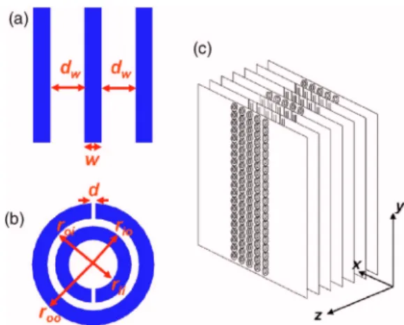
⬍a/2 since in this case both neffand meffacquires an enhancement. Instead, we employ a design in which the unit cell accommodates multiple wires. In this case, meff would roughly be the same 共since the wire radius did not change兲 but neffis multiplied by M, the number of wires. In addition, multiple wire pattern results in less absorption for the transmitting signal compared to that of the single thick wire designed for the samep.Figures 1共a兲 and 1共b兲 show one unit cell of the SRR and the wire micro-patterns, respectively. The unit cell of the CMM contains one SRR, and two layers of triple wire pat-tern. Employing two consecutive wire layers increases the coupling and the overall density of wires, which shifts p further higher. The dimensions of the components are as fol-lows: Inner ring inner radius: rii= 43m, inner ring outer radius: rio= 67.2m, outer ring inner radius: roi= 80.7m, outer ring outer radius: roo= 107.5m, split ring gap: d = 7.2m, wire width: w = 26.9m, wire separation: dw = 53.7m. The periodicity in x- and y-directions is ax= ay = 262.7m.
The metamaterial patterns are printed on glass substrates by employing UV-photolithography followed by microfabri-cation with a metal thickness of 100 Å Ti/ 4500 Å Au. For SRR-only and wire-only structures, plain glass layers 共de-noted as “glass” in the figures below兲 were used as spacers, so that the resulting periodicity is the same as in the CMM structure. All structures have 10 unit cells in the propagation direction. The CMM was composed of 100 layers, having a
15 mm 共100⫻150m兲 width 共z兲, 20 mm height 共y兲, and 2.6 mm length共x兲, x being the propagation direction. Figure 1共c兲 shows the schematic of the CMM, while Fig. 2 is a photomicrograph of one SRR-layer and stacked on top of one wire-layer. The patterns were aligned to the substrate edge during photolithography, thus, the alignment within the resulting metamaterial is limited by the edge uniformity of the substrate layers.
The transmission spectrum was measured by a millimeter wave network analyzer. Figure 3 shows the normal-to-the-plane transmission spectrum of SRR-only for two different SRR orientations. In this configuration, the resonance of SRR can be excited only through the electric field,13 when the SRR is asymmetric with respect to E 共lower three curves兲. Since the asymmetric orientation causes a misbal-ance of the charge distribution and induces circulating cur-rents on SRRs, the result is a resonant electric response of the system, which appears as a gap. On the other hand, the FIG. 1.共Color online兲 共a兲 Wire and 共b兲 SRR geometry employed for the CMM.共c兲 Schematic of the CMM, consisting of periodically stacked 共along z兲 two layers of wire-patterned substrates and one layer of SRR-patterned substrate. The propagation direction for the electromagnetic field is along the x axis.
FIG. 2. 共Color online兲 Photomicrograph showing the CMM sample. The SRR共front兲 and wire 共back兲 layers were aligned by the edges of the glass substrates.
BRIEF REPORTS PHYSICAL REVIEW B 73, 193103共2006兲
symmetric orientation with respect to E共upper three curves, marked in circle兲 is transparent. Increasing the number of layers enhances and, due to interlayer coupling between SRRs, widens the resonance gap. In order to avoid electric coupling, we employ the symmetric orientation in the CMM. Figure 4 shows the transmission spectra of wire-only, SRR-only, and closed ring resonator共CRR兲-only structures. The CRR is just the SRR with splits closed, and thus has no magnetic response. The legend denotes the components in one unit cell. The⬍0 stop-band of the wire-only structure spans the measured frequency range. The onset of transmis-sion above 120 GHz signals thepof wires. The SRR-only
structure exhibits a resonance 共⬍0兲 between 95 and 108 GHz with −30 dB minimum occurring at 102 GHz whereas the CRR-only medium is transparent, as expected.
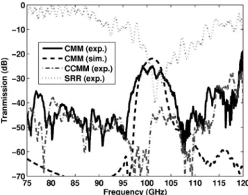
In order to contrast the CMM response, a “nonworking” CMM is made by replacing SRR layers with CRR layers 共called CCMM here兲.8 Figure 5 shows the measured trans-mission spectra of CMM structures incorporating SRRs 共black solid line兲, and CRRs 关blue 共gray兲 solid line兴, respec-tively. The simulated CMM transmission共dashed black line兲 will be discussed further below. The CMM structure exhibits a clear pass band between 96 and 107 GHz with a −25 dB FIG. 3. Transmission spectra of the SRR-only structure for
propagation normal to the SRR plane for different number of layers along the propagation direction with SRR-splits parallel 共upper three curves, marked in circle兲 and perpendicular 共lower three curves兲 to the electric field vector E. The resonant behaviour occurs in the latter case.
FIG. 4. Transmission spectra of CRR only共dashed line兲, SRR only共solid line兲, and wire only 共dash-dotted line兲 structures. The legend denotes the respective number of layers within one unit cell of the assembled structure. “Glass” is a plain glass substrate layer used as spacer.
FIG. 5. The experimental 共solid black line兲 and simulated 共dashed black line兲 transmission spectra of CMM. At around 100 GHz, the ⬍0 gap of the SRR-only structures 共dotted light gray line兲 matches the transmission band of the CMM. In contrast, the transmission spectra of the CCMM共dash-dotted gray line兲 is opaque in this range. The increase of the transmission at 120 GHz signals the onset of a right-handed transmission band共plasma cut-off frequency兲 for the CMM and CCMM.
FIG. 6.共Left axis兲 The real 共solid black兲 and imaginary 共dashed black兲 parts of the frequency dependent index of refraction com-puted by retrieval procedure.共Right axis兲 The dotted light gray line shows the measured transmission band of the CMM for comparison.
BRIEF REPORTS PHYSICAL REVIEW B 73, 193103共2006兲
maximum at 101 GHz. We stress that this band matches the
⬍0 stop band of SRRs 共shown by the light gray dotted line兲. On the other hand, the CCMM 关blue 共gray兲 solid line兴 remains opaque, because it is essentially a⬍0 medium.
The simulations are done by a commercial software共 MI-CROWAVE STUDIO兲 which employs the finite integration tech-nique for solving Maxwell’s equations. Two main assump-tions apply to the simulated structure:共i兲 The loss of metal and substrate are included by reference conductance values, and the finite thickness of the metal 共in relation to skin depth兲 is not considered. 共ii兲 Disorder is not included. As reported in a recent study,17fabrication-based nonuniformity of SRR and wire elements 共especially close to the mask edges兲, and misalignment induced by variations in substrate size are inherent problems, which may degrade the transmis-sion significantly. Nevertheless, the theoretical transmistransmis-sion spectrum for the CMM plotted in Fig. 5 shows good agree-ment with the experiagree-mental results. The calculatedpfor the wire-only structure is above 150 GHz; therefore, the wire spectrum is not shown. Figure 6 shows the refractive index, n, of the CMM computed through the retrieval procedure16 relative to the measured transmission spectra of a single layer CMM. The real part of n共f兲 is negative within the
transmission band of the CMM with a value of −5.2 at f = 100 GHz.
In conclusion, we have demonstrated the left-handed be-havior in the multilayer SRR+ wire type CMM at 100 GHz. The operation frequency is one order of magnitude above the previously reported values. The CMM was fabricated on glass-substrates, using photolithography, and microfabrica-tion. The transmission band of the CMM was located well within the ⬍0 stop-band of the structure, coincided with the ⬍0 stop-band of the SRR-only medium, and disap-peared when the splits of the SRRs were shorted, proving unambiguously its left-handed nature. The experimental re-sults are strongly supported by the theoretical simulations.
ACKNOWLEDGMENTS
This work was supported by the projects EU-DALHM,
EU-NOE-METAMORPHOSE, EU-NOE-PHOREMOST,
TUBITAK-104E090, DARPA-HR0011-05-C-0068, and Greek Ministry of Education PYTHAGORAS and by Ames Laboratory 共Contract No. W-7405-Eng-82兲. E.O. acknowl-edges partial support from the Turkish Academy of Sciences. The research of C.M.S. is further supported by the Alexander von Humboldt senior-scientist award 2002.
*Corresponding author. Electronic address: [email protected]
1V. G. Veselago, Sov. Phys. Usp. 10, 504共1968兲.
2D. R. Smith, W. J. Padilla, D. C. Vier, S. C. Nemat-Nasser, and S. Schultz, Phys. Rev. Lett. 84, 4184共2000兲.
3R. A. Shelby, D. R. Smith, S. C. Nemat-Nasser, and S. Schultz, Appl. Phys. Lett. 78, 480共2001兲.
4N. Engheta and R. W. Ziolkowski, IEEE Trans. Microwave Theory Tech. 53, 1535共2005兲.
5J. B. Pendry, Phys. Rev. Lett. 85, 3966共2000兲.
6J. B. Pendry, A. J. Holden, W. J. Stewart, and I. Youngs, Phys. Rev. Lett. 76, 4773共1996兲.
7J. B. Pendry, A. J. Holden, D. J. Robbins, and W. J. Stewart, IEEE Trans. Microwave Theory Tech. 47, 2075共1999兲. 8K. Aydin, K. Guven, M. Kafesaki, L. Zhang, C. M. Soukoulis,
and E. Ozbay, Opt. Lett. 29, 2623共2004兲.
9S. Linden, C. Enkrich, M. Wegener, J. Zhou, T. Koschny, and C. M. Soukoulis, Science 306, 1351共2004兲.
10T. J. Yen, W. J. Padilla, N. Fang, D. C. Vier, D. R. Smith, J. B. Pendry, D. N. Basov, and X. Zhang, Science 303, 1494共2004兲.
11N. Katsarakis, G. Konstantinidis, A. Kostopoulos, R. S. Penciu, T. F. Gundogdu, M. Kafesaki, E. N. Economou, T. Koschny, and C. M. Soukoulis, Opt. Lett. 30, 1348共2005兲.
12H. O. Moser, B. D. F. Casse, O. Wilhelmi, and B. T. Saw, Phys. Rev. Lett. 94, 063901共2005兲.
13N. Katsarakis, T. Koschny, M. Kafesaki, E. N. Economou, and C. M. Soukoulis, Appl. Phys. Lett. 84, 2943共2004兲.
14V. M. Shalaev, W. Cai, U. K. Chettiar, Hsiao-Kuan Yuan, A. K. Sarychev, V. P. Drachev, and A. V. Kildishev, Opt. Lett. 30, 3356共2005兲.
15T. Koschny, M. Kafesaki, E. N. Economou, and C. M. Soukoulis, Phys. Rev. Lett. 93, 107402共2004兲.
16D. R. Smith, D. C. Vier, T. Koschny, and C. M. Soukoulis, Phys. Rev. E 71, 036617共2005兲.
17K. Aydin, K. Guven, N. Katsarakis, C. M. Soukoulis, and E. Ozbay, Opt. Express 12, 5896共2004兲.
18M. Kafesaki, T. Koschny, R. S. Penciu, T. F. Gundogdu, E. N. Economou, and C. M. Soukoulis, J. Opt. A, Pure Appl. Opt. 7, S12共2005兲.
BRIEF REPORTS PHYSICAL REVIEW B 73, 193103共2006兲