PHYSICAL REVIEW B VOLUME 38, NUMBER 17
b
doping in strained
(SOl(Ge)
snperlattices
15DECEMBER 1988-I
S.
Ciraci*
IBMResearch Division, Zurich Research Laboratory, 8803Rkschlikon, Switzerland
Inder
P.
BatraIBMResearch Division, IBMAlmaden Research Center, 650Harry Road, San Jose, California 95120-6099
E.
TekmanDepartment
of
Physics, Biikent University, Biikent, 06533Ankara, Turkey (Received 1 August 1988)We present a comparative study of the pseudomorphic (Si)6/(Ge)6 and b-doped
(Si)3(Sb)(Si)2/(Ge)6 superlattices using the self-consistent pseudopotential method. The strained (Si)6/(Ge)6 superlattice has the lowest conduction-band states of extended character, and the difference of energy between the direct and indirect band gap is 70 meV. Upon 8doping by Sb
in the Sisublattice, aquasi-two-dimensional band confined to the Sb layer dips into the band gap. Furthermore, the average potential in the Ge sublattice rises relative to that ofthe Siside, which
increases the band offset, and enhances the localization ofthe quantum well states. These results
indicate that 8doping provides new means forcontrolling the electronic properties ofstrained su-perlattices.
Pseudomorphic
(Si)„/(Ge)„(n
~
6)
superlattices la-terally restricted totheSi(001)
surface have been grown' in spiteof
the large lattice mismatch(4%) of
constituent crystals. Recent studies' on these semiconductor het-erostructures have revealed novel electronic properties.It
was shown that the band lineup is strongly dependent on the lattice strain. ~s In(Si)„/(Ge)„(3(n~6)
the valence bandof
the Ge sublattice rises relative to that of the Si sublattice leading to a band offset ~F«. Ey,o,
—
Ey
s;,of
Q.84 eV. As a result carriers (electrons andholes) are separated in real space. While electrons are confined in the Si sublattice, holes are localized in Ge displaying a staggered type-II alignment. Most impor-tantly, direct optical transitions have been observed, ' which are found neither in constituent crystals, nor in
Si~
„Ge,
alloys. Currently, modifying the electronic structure ofSi
by varying the structural parametersof
a strained superlattice[(Si)
t,
(Ge)
j,
/[(Si)
~ «(Ge)«]and thus improving its electronic properties, has been ex-tensively studied. In an effort to incorporate optoelect-ronics into the Si-based microelectronics, the possibility of obtaining a direct-band semiconductor using a
(Si)/(Ge)
heterostructure has become a topic of major interest. A small oscillator strengthof
the lowest direct transition and the stabilityof
the heterostructure seem to present significant difficulties, however.An alternative way to control the band alignment and, thus, to modify the confined states in the
(Si)/(Ge)
quantum-well structure may be to incorporate an ex-tremely sharp and high-density doping pro61e. This type
of
doping iscalled b doping. An early suggestion that the band offsetof
a semiconductor heterostructure can be modified was demonstrated for the first time by Capasso, Cho, Mohammed, and Foy for Al Ga~ „As/GaAsheterojunction. A new type
of
nonalloyed Ohmic contactwith GaAs is achieved by placing a high-density donor sheet afew layers away from the metal-semiconductor in-terface. Zeindel et al.' have incorporated a sheet
of
Sb intoSi(001)
with an aerial densityof
—
1.
6&10'
Sb cm 2. They showed that this b layer gives rise toaquan-tum well with the confined states
of
electrons.The
8
doping is rather different from the modulation doping or bulk dopingof Si.
Upon the growthof
a high-density impurity sheet the excess carriers due to the im-purity atom are confined in the quantum well of the"finite" 8
layer, and give rise to the two-dimensional(2D)
subband structure.If
the thickness of the b' layer isre-duced to a single layer, the impurity states may be delo-calized and form a two-dimensional
(2D)
band restricted to this layer. The delocalizationof
impurity states and dispersion of the bands produced therefrom have to be dependent on the concentrationof
the dopant, and, thus, on the overlapof
nearest-neighbor impurity orbitals(p;(r)
(p;(r+D)&.
While the impurity band modifies theband gap, the charge distribution and the potential at the b layer may affect the band diagram
of
the heterostruc-ture. The form of the band diagram and the stabilityof
the8
layer against the exchange-place reaction have to vary according to its position. Therefore, significant vari-ances are anticipated depending upon whether the8
layer islocated at the interface orin one ofthe sublattices. The thickness and the impurity concentrationof
the b layer are also crucial parameters which influence the electronic structure.We have investigated the effect
of
the8
layer on the pseudomorphic(Si)„/(Ge)„superlattices.
In this paper, we present a comparative studyof
strained(Si)s/(Ge)s
and b-doped
(Si)3(Sb)(Si)2/(Ge)s
both restricted to theSi(001)
surface. The blayer here isidealized with one Sb atomic plane replacing the fourthSi
plane in the unit cell6DOPING IN STRAINED (Si)/(Ge) SUPERLAI I'ICES 12729
of
(Si)
s/(Ge)6, and is used only toexplore its eff'ect on the electronic structureof
the(Si)/(Ge)
superlattices. The important findings ofour study are(i)
the average poten-tial ofthe Ge sublattice rises relative to that ofSi,
which in turn increases the depth ofthe quantum well structure, and thus enhances the localizationof
the confined states, and (ii) the lowest conduction-band stateof
(Si)s/(Ge)6, which have almost equivalent weights in both sublattices(Si
andGe),
are replaced by a quasi-2D band confined to the Sblayer.It
is shown that the inclusion ofan ultrathin dopant layer can modify the band lineupof
the strained(Si)/(Ge)
superlattice.We have performed total-energy and charge-density calculations for
(Si)s/(Ge)6
and(Si)3(Sb)(Si)2/(Ge)s
by using the standard self-consistent field(SCF)
pseudopo-tential method with nonlocal, norm-conservingpseudopo-tentials"
and Ceperley-Alder exchange correlation ap-proximation. ' Other details about the method can be found elsewhere."
Bloch states are expanded in termsof
—
1500 plane waves corresponding to a kinetic energy cutoffof
~k+G
~~
13.
5 Ry.To
ensure the epitaxy, thelateral lattice constants are set equal to those
of
the idealSi(001)
surface[~RI
~(R2(
ao(Si)/J2,
ao(Si)
beingthe equilibrium lattice constant
of
bulkSi].
The equilibri-um lattice constant of bulk Si is calculated to be10.
24 a.u. The perpendicular lattice constants of (Si)s/(Ge)6 are determined by minimizing the total energy with respect to the structural degreesof
freedom. These are the Si-Ge and strained Ge-Ge interlayer spacin s. The superlattice formation energy of (Si)&/(Ge)s, &F. , is cal-culated from the total energies,ET
and ETo,ofthe super-lattice and constituent crystals, respectively,AFI((Si)6/(Ge)s)
ET((Si)s/(Ge)s)
—
[ET((»)
l2)+ET((Ge)12)]/2,
ture
of
the superlattices by applying a constant upward shiftof
0.
5eVtothe conduction-band energies. Using the same approach we calculated that the indirect band gapof
the strained (Si)4/(Ge)4 is0.
8 eV. The value for the same energy gap obtained from the local-density-functional and quasiparticle self-energy calculations by Hybertsen and Schliiter is0.
85 eV. An important char-acterof
the electronic structure, that is, the difference in the indirect and direct energy gap bEs, is affected by the zone folding' and the lattice strain. Bands along the b directionof
the cubic Brillouin zone(CBZ)
are folded for kll[001] (or k&) resulting in a decrease of bEs. In contrast, the bands at the topof
the valence band are split and the lowest conduction band atk
0
rises under the tetragonal strain of Ge, the net effect being an increase of BEs in the strained Ge. Finally, upon formationof
(Si)s/(Ge)s
the bands of the sublattices shift leading to the quantum wells with the flat conduction bands along the superlattice direction. While the states of these con-duction bands are confined in theSi
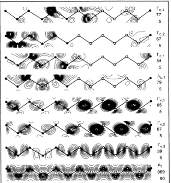
sublattice, first and second highest valence-band states are weakly locahzed in Ge. In Fig. 1,we present the contour plots of the total-and state-charge density for(Si)s/(Ge)z.
The quantum-well structure deduced from the localizationof
the states suggests that electron and hole quantum wells are located in Si and Ge, respectively. Because of the small electron mass and the small size ofthe quantum well, the statesof
the lowest conduction band for k [k& O,kllh, or IM
directionof
the superlattice Brillouin zone(SBZ)]
have an extended character, however. While the lowest direct'c,4 30 5 [c,2 58 5 wWmn 66 5 18 5 &+~LJ ~QgY Qg 'v,1 77 5 I O' 5 v3 34 5 PT 873 90
FIG. 1. Contour plots of the total- and state-charge density
of (Si)4/(Ge)4. pr is the total-charge density.
I.
,& andI,
,&denote the topmost valence and the lowest conduction-band states at the 1 point, respectively. Upper and lower numerals
in-dicate the value of the maximum charge density (in 10 xelectrons &bohr 3)and contour spacings, respectively.
and is found to be
9.
29 mRy/cell favoring the separation into constituent crystals. This structure is metastable be-cause the activation energy either for segregation or for the generation of the misfit dislocation is larger than(n
6).
The interfacial energy ofthe Si-Geinterface iscalculated to be-0.
5mRy. The strain energy stored in the Ge sublattice, which dominates AFI, is found to be proportional to n, and is1.
46mRy per Ge atom.There-fore,
~
(n)
increases with increasing nIn.
(Si)3(Sb)(Si)2/(Ge)s,
the interlayer spacing between the adjacentSi
and Sbatomic planes isfixed tothe sumof
the covalent radiiof Si
and Sb. Other structural parameters [the lateral lattice constants of the(001)
cell,IR~ IR~
7.
24 a.u.; the interlayer spacing in theSi
sublattice,d(Si-Si)=2.
56a.
u.; the interlayer spacing at the interface,d(Si-Ge)
2.60a.
u.; and the interlayer spac-ing in the Gesublattice,d(Ge-Ge)
=2.
70
a.
u.]
are taken to bethe same asin(Si)6/(Ge)6.
Having determined the structural parameters we dis-cuss the electronic structure
of (Si)s/(Ge)6.
TheSCF
pseudopotential method within the local-density approach underestimates the conduction-band energies. However, the average error in bulkSi
and Geis-0.
5eV forthe ki-netic energy cutoff, ~k+G
~~
13.
5 Ry. Therefore, thestruc-12730
S.
CIRACI, INDER P.BATRA, ANDE.
TEKMANtransition I
„~
I,
~occurs at0.
84eVwith asmalloscil-lator strength, the lowest value ofthe band gap is
0.
77eV between I„and
b,
;„.
Accordingly, the energy gapof
the(Si)s/(Ge)s
superlattice is found tobe indirect (bEg)
0).
A more significant finding, however, is that the energy separation between the direct and indirect band gapof
Si decreases from-2
to0.
07 eV.The integration ofthe planarly averaged charge density E~Ep.
p(z)-
„",
"
'„,
"
'
g
[Iv. (k, r)~'dxdy
ggigV~o
~+U~(%Fr'
'c,4 77 Ic, 2 67 'c,i 54between two consecutive atomic
(001)
planes, landl+
1, ~I+~q(l+
l,
l)
p(z)dz
2
~I
shows small deviations from the ideal bulk value
(4+'0.
02 electrons). This implies that the transferof
charge upon superlattice formation israther small.The question we shall address next is how the electronic structure
of
the(Si)s/(Ge)6
superlattice is modified when one Si atomic layer(i.e.
, fourth layer in the unit cell) is replaced bySb.
The amountof
electronic charge between the adjacent(Si)3-(Sb)
and(Sb)-(Si)5
(001)
atomic planes is found to be4.
51 and4.
56 electrons per atom. These self-consistent valuesof
q((Si)
3,(Sb)
)
andq((Sb), (Si)5)
indicate that the simple bond picture pre-dicting the excess chargeof
Q—
e(Z
—
4)/2(Z
being the valencyof
the dopant atom) is approximately valid, except for asmall deviationof
0.
07electrons. On the oth-er hand, we calculated that a small amountof
charge is transferred from one side[(Si)3(Sb)(Si)2]
to the adjacent Ge side of the superstructure, which leads to a relative shift in the average potential energiesVof
two sublattices.The potential, consisting
of
the local partof
the ionic pseudopotential, Hartree, and exchange potentials, are planarly averaged and, thus, the 1DpotentialV(z)
is gen-erated. The averageof V(z)
is calculated in the adjacent sublattices Vs;and Vo,.
The differenceof
the average po-tentials Vs;-VG,hV
is found to decrease by90
meV upon b doping, implying that the electronic statesof
the Ge sublattice rise (or thoseof
theSi
sublattice are lowered). This causes the band offset,~y,
of(Si)s/(Ge)s
to increase from0.
84 to0.
93
eV upon the b doping. As a result, the depth of the quantum well (for both electron and hole) increases, but the band gapof
the superlattice decreases. The effectof
the relative shift in the average potential energiesof
the sublattices, hV, is seen in the charge density and electronic band structure of(Sl)
3(Sb
) (Sl )
2/(Ge)s.The contour plots
of
the total- and state-charge density for(Si)3(Sb)(Si)2/(Ge)s
are shown in Fig.2.
The locali-zationof
the states at the topof
the valence band are significantly increased as compared to thoseof
(Si)s/(Ge)s
illustrated in Fig.1.
The extended statesof
(Si)s/(Ge)s
along the6
direction and near theX
pointof
theCBZ
withkll(001)
are replaced by aquasi 2Dband of the b layer, and become localized on the(Si)3(Sb)(Si)2
side. Along the IZ
directionof
SBZ
the first and second conduction-band states are also confined to theSi
side, and their charge distributions do not differ significantlyf'I 86 4%l ' 4%I 5 t'v2 &rKr 5 'v,3 39 PT 869 90
FIG.2. Contour plots ofthe total- and state-charge density
of(Si)3(Sb)(Si)2/(Ge)6.
L
Z
I'
MFIG.3. Energy band structure of (Si)3(Sb)(Si)2/(Ge)6. The zero ofenergy isset to the average energy ofthe topmost three
valence-band states. The inset shows the superlattice Brillouin zone, where the 1Mdirection corresfmnds to the h, direction of CBZ. The 2D band originating from the 8' layer is shown by
b DOPING IN STRAINED (Si)l(Ge) SUPERLA'I I ICES 12731
from those
of (Si)s/(Ge)s.
These states are derived from the Si sublattice. Similarly, the third conduction-band state islocalized at the interface and in the Ge sublattice. However, the fourth conduction-band state has a strong weight near theSi
—
Sb
—
Si
bonds, and is associated with the8
layer.The band structure
of
(Si)s(Sb)(Si)g(Ge)s
in Fig. 3 displays the minizone with flat bands fork& (shown in therZ
direction). In contrast to(Si)g(Ge)s
the lowest con-duction band along the IM
direction is lowered and has a minimum at theM
point ofSBZ.
Owing to factors such as the loweringof
the lowest conduction band and the band energiesof
the Ge sublattice, the indirect band gap is decreased. Certainly, the effectsof
those factors on the band gap is proportional to the concentrationof
the dopant. In the present study the Sb monolayer has max-imum concentration (or minimumSb-Sb
distance), and thus the largest effect in reducing the band gap. Sincethe excess charge(Z
—
4)
is one electron per cell, the Fermi level crosses the conduction band rendering the metalliza-tionof
the superlattice. However, at comparatively lower dopant concentration, the occupancy of the lowest con-duction band is significantly reduced. Recently, Zeindl etal.' simulated the Sb sheet, which they incorporated in the
Si(001)
sample, bySb+
ions uniformly distributed in a-20-a.
u. -thick slab leading to a quantum well. They carried out self-consistent calculations within the effective mass approximation, and obtained four subbands. Since the planeof
Sb atoms in the present model cannot be treated as a quantum well, our states associated with the b layer are not comparable with these subbands. However, our results show similar trends, such as the loweringof
the band gap and localizationof
the lowest conduction-band states atthe Sblayer.In conclusion, we have shown that a monolayer
of
Sb lattice matched to theSi
sublattice in a pseudomorphic(Si)g(Ge)s
superlattice leads to important changes in the electronic structure. The monolayer doping is only an idealized model, and is unstable as far as the energyof
formation is concerned.It
gives rise to aquasi 2D metal-licband, and increases the band offset. While the b dop-ing with high dopant concentration and finite thickness provides Ohmic contacts, it can also be used to alter the electronic properties of heterostructures, and to obtain new device characteristics at comparatively lower dopant concentrations.'Permanent address: Department ofPhysics, Bilkent
Universi-ty, Bilkent, 06533Ankara, Turkey.
'T.
P.Pearsall,J.
Bevk, L.C.Feldman,J.
M.Bonar,J.
P. Man-naerts, and A. Ourmazd, Phys. Rev.Lett. 58, 729(1987). C.G.Van de Walle andR.
M.Martin,J.
Vac.Sci.Technol. B3, 1256(1985).
sS.Ciraci and
I.
P.Batra, Phys. Rev. Lett. 58, 2114(1987); S. Ciraci andI.
P.Batra, Phys. Rev. B 38, 1835(1988); S. Cira-ci,O.Giilseren, and$.
Ellialtioglu, Solid State Commun. 65,1285(1988).
4S.Froyen, D. M.Wood, and A.Zunger, Phys. Rev. B36, 4574 (1987); R.People and
S.
A.Jackson, ibid 36,1310(1.
987);I.
Morrison and M.Jaros, ibid 37,916 (1.988).
5M.
S.
Hybertsen and M. Schluter, Phys. Rev. B 36, 9683 (1987);L. Brey and C. Tejedor, Phys. Rev. Lett. 59, 1022 (1987).G, Abstreiter, H.Burgger, T.Wolf, H.Jorke, and H. Herzog, Phys. Rev.Lett. 54,2441
(1985).
7D.Streit, R.A.Metzger, and
F.
6.
Allen, Appl. Phys. Lett. 44, 234(1984).F.Caposso, A.Y.Cho, K.Mohammed, and P. W.Foy, Appl. Phys. Lett. 46, 664 (1985).
E. F.Schubert,
J.
E.Cunningham, W.S.
Tsang, and T. H. Chiu, Appl. Phys. Lett. 49,272(1986).
' H. P. Zeindl, T.Wegehaupt,
I.
Eisele, H. Oppolzer, H. Res-inger, G. Tempel, andF.
Koch, Appl. Phys. Lett. 50, 1164 (1987)."C.
B.Bachelet, D.R.Hamann, and M.Schluter, Phys. Rev.B 26,419(1982).' D. M. Ceperley and B.
J.
Adler, Phys. Rev. Lett. 45, 566 (1980).' The details of the calculations and references related to the
method can befound in
I.
P.Batra,S.
Ciraci,6.
P.Sirivasta-va,