ELECTRIC FIELD DEPENDENT
OPTOELECTRONIC NATURE OF
InGaN/GaN QUANTUM STRUCTURES AND
DEVICES
A THESIS
SUBMITTED TO THE DEPARTMENT OF ELECTRICAL AND ELECTRONICS ENGINEERING
AND THE GRADUATE SCHOOL OF ENGINEERING AND SCIENCE OF BILKENT UNIVERSITY
IN PARTIAL FULLFILMENT OF THE REQUIREMENTS FOR THE DEGREE OF
DOCTOR OF PHILIOSOPHY
By
Emre Sarı
December 2012
ii
I certify that I have read this thesis and that in my opinion it is fully adequate, in scope and in quality, as a thesis for the degree of Doctor of Philosophy.
Assoc. Prof. Hilmi Volkan Demir (Supervisor)
I certify that I have read this thesis and that in my opinion it is fully adequate, in scope and in quality, as a thesis for the degree of Doctor of Philosophy.
Prof. Ömer Morgül
I certify that I have read this thesis and that in my opinion it is fully adequate, in scope and in quality, as a thesis for the degree of Doctor of Philosophy.
iii
I certify that I have read this thesis and that in my opinion it is fully adequate, in scope and in quality, as a thesis for the degree of Doctor of Philosophy.
Assoc. Prof. Dönüş Tuncel
I certify that I have read this thesis and that in my opinion it is fully adequate, in scope and in quality, as a thesis for the degree of Doctor of Philosophy.
Assoc. Prof. Hamza Kurt
Approved for the Graduate School of Engineering and Science:
Prof. Levent Onural
iv
ABSTRACT
ELECTRIC FIELD DEPENDENT OPTOELECTRONIC
NATURE OF InGaN/GaN QUANTUM STRUCTURES
AND DEVICES
Emre Sarı
Ph.D. in Electrical and Electronics Engineering
Supervisor: Assoc. Prof. Hilmi Volkan Demir
December 2012
In the past two decades we have been witnessing the emergence and rapid development of III-Nitride based optoelectronic devices including InGaN/GaN light-emitting diodes (LEDs) and laser diodes with operation wavelengths ranging from green-blue to near-UV. These InGaN/GaN devices are now being widely used in applications important for lighting, displays, and data storage, collectively exceeding a total market size of 10 billion USD. Although InGaN/GaN has been studied and exploited very extensively to date, its field dependent nature is mostly unknown and is surprisingly prone to quite unexpected behavior due to its intrinsic polarization property. In this thesis, we report our systematic study on the electric field dependent characteristics of InGaN/GaN quantum structures and devices including modulators and LEDs. Here we present our comparative study of electroabsorption in polar c-plane InGaN/GaN multiple quantum wells (MQWs) with different built-in polarization induced electrostatic fields. Analyzing modulator structures with varying structural MQW parameters, we find that electroabsorption grows stronger with decreasing built-in electrostatic field strength inside the well layer, as predicted by our theoretical model and verified by our experimental results. To further explore the field dependent optoelectronic nature of c-plane grown InGaN/GaN quantum structures, we investigate radiative carrier dynamics, which is of critical importance for LEDs. Our time and spectrum resolved
v
photoluminescence measurements and numerical analyses indicate that the carrier lifetimes, the radiative recombination lifetimes, and the quantum efficiencies all decrease with increasing field. We also study the physics of electroabsorption and carrier dynamics in InGaN/GaN quantum heterostructures grown intentionally on nonpolar a-plane of the wurtzite crystal structure, which are free of the polarization-induced electrostatic fields. We compare these results with the conventional c-plane grown polar structures. In the polar case, we observe blue-shifting absorption profile and decreasing carrier lifetimes with increasing electric field. In the nonpolar case, however, we observe completely the opposite: a red-shifting absorption profile and increasing carrier lifetimes. We explain these observations in the context of basic physical principles including Fermi‟s golden rule and quantum-confined Stark effect. Also, we present electroabsorption behavior of InGaN/GaN quantum structures grown using epitaxial lateral overgrowth (ELOG) in correlation with their dislocation density levels and in comparison to steady state and time-resolved photoluminescence measurements. The results reveal that ELOG structures with decreasing mask stripe widths exhibit stronger electroabsorption performance. While keeping the ELOG window widths constant, compared to photoluminescence behavior, however, electroabsorption surprisingly exhibits the largest performance variation, making the electroabsorption the most sensitive to the mask stripe widths. This thesis work provides significant insight and important information for the optoelectronics of InGaN/GaN quantum structures and devices to better understand their field dependent nature.
vi
ÖZET
InGaN/GaN KUVANTUM YAPILARININ VE
AYGITLARININ ELEKTRĠK ALANA BAĞLI
OPTOELEKTRONĠK DOĞASI
Emre Sarı
Elektrik ve Elektronik Mühendisliği Bölümü Doktora Tez Yöneticisi: Doç. Dr. Hilmi Volkan Demir
Aralık 2012
Geride bıraktığımız 20 yılda, çalışma dalgaboyları yeşilden yakın morötesine değişen InGaN/GaN tabanlı ışık yayan diyotlar (LED'ler) ve lazer diyotlar gibi III-Nitrür tabanlı optelektronik aygıtların ortaya çıkışına ve hızlı bir şekilde gelişimine şahit olduk. Bu InGaN/GaN tabanlı aygıtlar artık görüntü, veri saklama ve aydınlatma gibi birçok alan için önem arz ediyor ve toplamda 10 milyar Amerikan dolarının üzerinde bir pazar büyüklüğü oluşturuyor. Bu InGaN/GaN yapıları şimdiye kadar yoğun olarak araştırılmış ve incelenmiş olsa da elektrik alana bağlı doğası çoğunlukla bilinmemektedir; kendinden kutuplu olma özelliği sebebiyle beklenmeyen davranışlar göstermeye eğilimlidir. Bu tez çalışmasında InGaN/GaN kuvantum yapılarının ve bunları içeren kipleyici ve LED gibi aygıtların elektrik alana bağlı özelliklerini incelediğimiz sistematik çalışmalarımızı sunmaktayız. Farklı yapısal özelliklere sahip çoklu kuvantum kuyusu (MQW) içeren kipleyici yapılarını inceleyerek, teorik modelimizle ve deneysel sonuçlarımızla uyumlu şekide, kendinden polarizasyon sebepli elektrik alan şiddeti azaldıkça elektrosoğrulmanın güçlendiğini bulduk. c-düzlemine büyütülmüş InGaN/GaN kuvantum yapılarının elektrik alana bağlı optoelektronik doğasını daha derinlemesine incelemek için LED'ler için kritik önem arz eden ışınımsal taşıyıcı dinamiğini inceledik. Zaman ve tayf çözünümlü fotoışıma ölçümlerimiz ve sayısal analizlerimiz taşıyıcı ömürlerinin, ışınımsal
vii
taşıyıcı ömürlerinin ve kuvantum verimliliklerinin hepsinin artan elektrik alan ile azaldığını gösterdi. Ayrıca wurtzite kristal yapısının polarizasyon sebepli elektrik alan içermeyen, polar olmayan, a-düzlemine büyütülen InGaN/GaN kuvantum yapılarının elektrosoğrulma ve taşıyıcı dinamiği ile ilgili fiziğini çalıştık. Buradan elde ettiğimiz sonuçları geleneksel olarak kullanılan c-düzlemine büyütülen polar yapılarla karşılaştırdık. Polar durumda artan elektrik alan ile maviye kayan soğrulma profili ve azalan taşıyıcı ömrü gözlemledik. Polar olmayan durumda, öte yandan, tamamen tersi olduğunu gösterdik: kırmızıya kayan soğrulma profili ve artan taşıyıcı ömürlerini bulduk. Bu gözlemlerimizi Fermi'nin altın kuralı ve kuvantum-kısıtlamalı Stark etkisi gibi temel fiziksel prensiplerle açıkladık. Ayrıca epitaksiyel yatay üst-büyütme (ELOG) tekniği kullanılarak dislokasyon yoğunluğu ile bağıntılı olarak InGaN/GaN kuvantum yapılarının elektrosoğrulma davranışını inceledik ve sabit hal ve zaman çözünürlüklü fotoışıma ölçümleriyle karşlaştırdık. Sonuçlarımız ELOG maske çizgi genişliğinin azalmasıyla elektrosoğrulmanın güçlendiğini gösterdi. ELOG pencere genişliğini sabit tutarken elektrosoğrulma performansı, ilginç bir biçimde, fotoışıma performansına göre daha çok değişim gösterip, elektrosoğrulmayı maske çizgi genişliğine daha hassas hale getirdi. Bu tez, InGaN/GaN kuvantum yapılarının ve aygıtlarının optoelekroniğinin, elektrik alana bağlı doğasını daha iyi anlaşılması için önemli içgörü ve önemli bilgi içermektedir.
Anahtar Kelimeler: Optoelektronik, III-Nitrürler, yarıiletkenler, kipleyiciler,
viii
Acknowledgements
I would like to take this opportunity to express my gratitude to Prof. Hilmi Volkan Demir, my supervisor and mentor, whose support, motivation and guidance made this thesis work along with other great things possible.
I would like to thank my committee members Prof. Ömer Morgül, Prof. Ali Kemal Okyay, Prof. Dönüş Tuncel and Prof. Hamza Kurt for accepting to be in my thesis jury.
I would like to thank TUBITAK BIDEB for their support from 2211 and 2214 programs.
Last but not the least; I would like to thank my friends and family for always being there especially to my wife, Serpil, whose support and endurance has been the inspiration to finalize this thesis. This thesis is dedicated to her…
ix
Table of Contents
1. ACKNOWLEDGEMENTS ... VIII
2. INTRODUCTION ... 1
3. BACKGROUND ... 6
2.1III-NITRIDES BACKGROUND ... 7
2.1.1SHORT HISTORY OF III-NITRIDES ... 7
2.1.2PHYSICAL PROPERTIES OF III-NITRIDES ... 10
2.1.3GROWTH OF III-NITRIDES ... 15
2.2OPTOELECTRONIC DEVICES BACKGROUND... 18
2.2.2ELECTROABSORPTION IN SEMICONDUCTORS ... 21
2.2.3LEDMODEL USED ... 25
2.3III-NITRIDE OPTOELECTRONIC DEVICES ... 26
2.3.1INGAN/GAN BASED VISIBLE LEDS ... 26
2.3.2INGAN/GAN BASED ELECTROABSORPTION MODULATORS ... 31
2.4SUMMARY ... 34
4. EPITAXIAL LATERAL OVERGROWN INGAN/GAN QUANTUM STRUCTURES ... 35
3.1INTRODUCTION ... 36
3.2EXPERIMENTS, RESULTS AND DISCUSSION... 37
DEVICE FABRICATION ... 38
MATERIALS CHARACTERIZATION ... 42
DEVICE CHARACTERIZATION ... 46
3.3SUMMARY ... 50
5. ELECTROABSORPTION OF INGAN/GAN QUANTUM STRUCTURES ... 51
4.1COMPARATIVE STUDY OF ELECTROABSORPTION IN INGAN/GAN QUANTUM STRUCTURES 51 4.2OPPOSITE ELECTROABSORPTION BEHAVIOR IN POLAR VS. NONPOLAR INGAN/GAN QUANTUM STRUCTURES ... 58
4.3SUMMARY ... 62
6. ELECTRIC FIELD DEPENDENT CARRIER DYNAMICS IN INGAN/GAN QUANTUM STRUCTURES ... 63
5.1ELECTRIC FIELD DEPENDENT RADIATIVE CARRIER DYNAMICS IN INGAN/GAN QUANTUM STRUCTURES ... 63
5.2OPPOSITE CARRIER DYNAMICS BEHAVIOR IN POLAR VS. NONPOLAR INGAN/GAN ... 70
5.3SUMMARY ... 77
7. ELECTRON BLOCKING LAYERS FOR INGAN / GAN BASED LEDS WITH LOW DROOP ... 78
6.1INTRODUCTION ... 78
6.2DESIGNS,SIMULATIONS,RESULTS AND DISCUSSIONS ... 79
6.3SUMMARY ... 84
8. CONCLUSIONS ... 85
9. SCIENTIFIC CONTRIBUTIONS ... 87
JOURNAL PAPERS ... 87
x
List of Figures
Figure 1. 1 Packaged LED revenues for different applications: Years 2008-2020. Note that the general lighting application is expected to dominate the market. After [4]. ... 2 Figure 2. 1 Cartoon showing the cross-section of the high quality buffer layer developed by Akasaki. After [1], [6]. ... 8 Figure 2. 2 CRIUS-II close coupled showerhead MOCVD reactor. A state of the
art tool for high throughput GaN growth. After [9]. ... 9 Figure 2. 3 Wurtzite crystal structure of GaN. Open circles indicate Ga atoms,
closed circles show N for Ga-face material. After [11]. ... 10 Figure 2. 4 Representative band diagram calculated for an In0.15Ga0.85N/GaN
quantum structure, here the quantum well and barrier thicknesses are 4 nm. ... 13 Figure 2. 5 (a) Polar, (b) and (c) nonpolar and (d) and (e) semipolar planes of
wurtzite GaN crystal structure. Ga atoms are represented by yellow atoms and nitrogen atoms are represented by blue balls. After [15]... 15 Figure 2. 6 Interband (band-to-band) absorption (carrier generation) in a
semiconductor. An electron in the valence band is raised to another state in the conduction band by a photon. After [32]. ... 19 Figure 2. 7 Interband (band-to-band) recombination mechanisms. Reproduced
after [1]. ... 20 Figure 2. 8 Schematic representation of Franz Keldysh effect. Courtesy of Prof.
David Miller. ... 22 Figure 2. 9 Electron and hole states in an infinite quantum well with zero
external electric field and non-zero electric field. Courtesy of Prof. David Miller. ... 23 Figure 2. 10 Optical absorption spectra for AlGaAs/GaAs quantum well
structure for various electric fields applied perpendicular across quantum well layers measured at room temperature. The spectra are shifted
vertically to dashed levels for clarity. Courtesy of Prof. David Miller. ... 24 Figure 2. 11 Band diagrams of two LEDs incorporating (a) an undoped AlGaN
EBL and (b) a p-doped AlGaN EBL. After [33]. ... 27 Figure 2. 12 LED efficiency vs. current and LED power vs. current (inset)
curves of a typical LED with droop and ideal LED with no droop. After [44]. ... 28 Figure 2. 13 The Schematics illustrating three structures studied in Ref. [51]: (a)
the conventional structure with constant AlN molar ratio of 20% (structure A) , (b) the normal superlattice structure with constant AlN molar ratio of
xi
20% (structure B) and (c) the gradual superlattice structure with triangular
AlN molar ratio (0-20-0%) (structure C). After [51]. ... 29
Figure 2. 14 Band diagrams and carrier concentrations of structures A, B and C at the current density of 200 A/cm2. After [51]. ... 30
Figure 2. 15 Dependence of internal quantum efficiency (or LED efficiency) on the current density showing droop levels for the structures. After [51]. .... 31
Figure 2. 16 Energy band diagrams of an InGaN/GaN quantum structure for zero external electric field case and non-zero external electric field case. After [52]. ... 32
Figure 2. 17 Absorption spectra of our EAM at 0-6 V levels. The absorption edge shows a clear blueshift with increasing external electric field. Reproduced after [52]. ... 33
Figure 2. 18 Absorption coefficient change with respect to 0 V absorption curve. After [52]. ... 33
Figure 3. 1 Schematic of one-step ELOG process. After [55]. ... 36
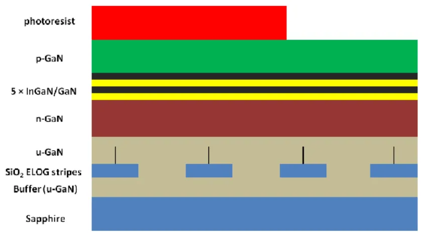
Figure 3. 2 Cartoon showing the cross-section of an ELOG sample before device fabrication. The lines on top of the SiO2 ELOG stripes represent coalescence walls. ... 38
Figure 3. 3 Photolithography procedure: mask is placed on the sample which was previously coated with photoresist, UV light is then applied. ... 39
Figure 3. 4 Sample after photolithography and subsequent development... 39
Figure 3. 5 Sample after mesa etching procedure (using RIE) and cleaning of the photoresist. The sample is etched down to n-GaN layer. ... 40
Figure 3. 6 Sample after n-contact deposition and annealing. ... 41
Figure 3. 7 Sample p-contact deposition and annealing. ... 41
Figure 3. 8 Sample after p-pad deposition. Sample is ready for test. ... 42
Figure 3. 9 Micrograph of a fabricated device comprising 4 μm mask and window widths ... 42
Figure 3. 10 Representative parts of the analyzed SEM images of the top surface of our epi-structures after etch pit formation: (a) reference sample, and ELOG samples with (b) 4 µm, (c) 7 µm, and (d) 10 µm wide stripes. ... 43
Figure 3. 11 PL spectra of (a) reference sample, and ELOG samples with (b) 4 µm, (c) 7 µm and (d) 10 µm wide stripes. ... 44
Figure 3. 12 Time-resolved photoluminescence decay profiles of our epitaxial lateral overgrowth structures and the reference sample along with their corresponding fits. The fastest decay profile corresponds to the reference sample due to its higher dislocation density, and thus higher nonradiative recombination rate. ... 45
Figure 3. 13 Comparison of (a) dislocation densities measured by SEM analysis and (b) recombination rates of our structures measured by TRPL analysis. ... 46
Figure 3. 14 Schematics and flow chart of our photocurrent measurement setup. ... 47 Figure 3. 15 Comparison of similar trends in (a) PL peak wavelengths and (b)
xii
peak FWHMs and (d) electroabsorption FWHMs; and (d) PL peak
intensities and (e) maximum photocurrent change among our structures. . 49 Figure 4. 1 Electroabsorption spectra of sample A under different bias voltages.
The inset (a) shows the absorption coefficient change for sample A with respect to the 0 V absorption curve and the inset (b) depicts the absorption spectra of sample A for 0, −1, and +1 V bias voltages. After [14]. ... 56 Figure 4. 2 Electroabsorption spectra of sample B under different bias voltages.
The inset (a) shows the absorption coefficient change for sample B with respect to the 0 V absorption curve and the inset (b) depicts the absorption spectra of sample B for 0, −1, and +1 V bias voltages. After [14] ... 56 Figure 4. 3 Electroabsorption spectra of sample C under different bias voltages.
The inset (a) shows the absorption coefficient change for sample C with respect to the 0 V absorption curve and the inset (b) depicts the absorption spectra of sample C for 0, −1, and +1 V bias voltages. After [14]. ... 57 Figure 4. 4 Normalized photoluminescence spectra of our InGaN/GaN based
polar and nonpolar quantum heterostructures at room temperature. After [73]. ... 60 Figure 4. 5 Normalized electroluminescence spectra of our devices based on
polar and nonpolar InGaN/GaN quantum heterostructures, both measured at a constant driving current of 20 mA at room temperature. After [73]. .. 60 Figure 4. 6 Photocurrent spectra of our device based on polar InGaN/GaN
quantum heterostructures. The arrow indicates the blue shift of the
absorption edge with the increasing reverse bias. After [73]. ... 61 Figure 4. 7 Photocurrent spectra of our device based on nonpolar InGaN/GaN
quantum heterostructures. The arrow indicates the red shift of the
absorption edge with the increasing reverse bias. After [73]. ... 61 Figure 5. 1 FluoTime 200 TRPL setup at our Lab. ... 65 Figure 5. 2 TRPL decay curves of our polar InGaN/GaN quantum
heterostructure under different electric field levels. The inset shows the carrier lifetime vs. applied electric field as a result of the TRPL analysis. After [67]. ... 66 Figure 5. 3 Steady-state PL spectra of our polar InGaN/GaN quantum
heterostructure under different electric field levels. The integrated PL intensity for the corresponding electric field level is presented in the inset. After [67]. ... 68 Figure 5. 4 Normalized PL spectra of our polar InGaN/GaN quantum
heterostructure under electric field. We observe a narrowing of the spectra along with a blueshift in the longer wavelength region, with a zoom-in presented in the inset for clarity. After [67]. ... 69 Figure 5. 5 Relative radiative recombination lifetime extracted from TRPL and
PL measurements. The inset shows energy band diagrams corresponding electron and hole ground state wavefunctions for the case of 0 V/μm and 12.5 V/μm externally applied electric field. After [67]. ... 70
xiii
Figure 5. 6 Room temperature time-resolved photoluminescence traces and numerical fits of our device with polar InGaN/GaN quantum
heterostructures under different bias levels. After [73]. ... 74
Figure 5. 7 Room temperature time-resolved photoluminescence (RT-TRPL) traces and numerical fits of our device with nonpolar InGaN/GaN quantum heterostructures under different bias levels. After [73]. ... 75
Figure 5. 8 Carrier lifetime (τ) vs external electric field (E) for the polar and nonpolar devices. Note that here E is taken to be positive for the forward bias and negative for the reverse bias. After [73]. ... 76
Figure 6. 1 Schematics showing the AlN molar ratio profile of our superlinear superlattice EBL design. ... 79
Figure 6. 2 LED efficiency vs current curves of the simulated structures. Our superlinear superlattice EBL design outperforms the structures with no EBL. ... 80
Figure 6. 3 Droop levels of the structures simulated. 10-0 is the best performing structure. ... 81
Figure 6. 4 Electron concentrations throughout the active regions. ... 81
Figure 6. 5 Hole concentrations throughout the active regions. ... 82
Figure 6. 6 Electron leakage levels of the samples. ... 82
Figure 6. 7 Hole concentration in the last quantum well layer. ... 83
1
Chapter 1
Introduction
Electronic devices based on silicon microelectronics technology have revolutionized the world we live in. Personal computers, and later mobile communication devices, including tablet computers and smart phones have made a significant impact on our lives. These tools are now much more capable compared to the past, thanks to ever-improving complementary metal-oxide-semiconductor (CMOS) microchip technology based on silicon. As a natural result, the size of electronics market and that of related areas such as telecommunication and information technology have constantly evolved and expanded. Related products and services have become more accessible especially in the last decade since the beginning of the 21st century.
In a similar way, we have been witnessing the emergence, increased interest of research and development, as well as the commercialization and wide usage of optoelectronic devices based on GaN in the same time interval [1]. Among those optoelectronic devices, light-emitting diodes (LEDs) with emission wavelengths varying from blue/green to ultraviolet (UV), and laser diodes (LDs) operating in blue and near-UV have achieved the biggest success. Today, we widely use LEDs
2
for liquid crystal display backlighting as well as traffic signs and white light sources. With the Blu-ray disc technology which utilizes GaN based blue LDs, we can now store more than 100 GB of information into a 12 cm diameter disc. Among GaN based optoelectronic devices demonstrated thus far, LEDs have achieved the widest usage so far, and are expected to have the most impact, among III-Nitride devices, especially through high efficiency solid state lighting. Currently, lighting consumes more than 20% of electricity produced in the world. US Department of Energy estimates that about US$ 100 Billion saving in energy can be realized by 2020, using 200 lm/W solid-state light sources (which are 20-50 times more efficient than incandescent light sources and 3-4 times more efficient than compact fluorescent lamps) for general lighting [2]. More importantly, a vast amount of reduction in carbon emission, many hundreds of million tons per year, can be achieved. Today, in the market, there are products with 165 lm/W luminous efficacies, and R&D records have exceeded 250 lm/W
[3]. Companies and research institutions are continuing to push the limits of the
device performances while reducing the costs associated with the technology.
Figure 1. 1 Packaged LED revenues for different applications: Years 2008-2020. Note that the general lighting application is expected to dominate the market. After [4].
3
Not surprisingly, the economic opportunities are enormous. The overall packaged LED market today is US$ 12 Billion, projected to be US$ 17 Billion by 2018 as shown in Figure 2.1. Although today the market is driven by the demand from the LCD display and general lighting segments equally (comprising more than 50% of the revenues), the general lighting segment is expected to dominate the LED market with its US$ 10 Billion projected share by the year 2018 [4].
Our group has been active in this device platform and contributed to hybrid LED research for high quality lighting in the last 6 years [5]–[9].
This thesis work is on InGaN/GaN quantum structures and devices that house them. In this thesis work, we present our studies on understanding the underpinning physics and improving the performances of electroabsorption modulators and LEDs. We study electroabsorption and electric field dependent carrier dynamics in epitaxial lateral overgrown (ELOG) and conventional polar c-plane structures and nonpolar structures. Furthermore, we present our results on the reduction of droop (the decrease of LED efficiency at high currents) in LEDs through multiple quantum well (MQW) to electron blocking layer (EBL) distance optimization.
In Chapter 2, we present a background on III-Nitride material platform its physical properties, history, and plausible future. We provide information on the crystal structures of III-Nitrides and explicate the polarization effects in their quantum structures, which cause built-in electrostatic fields in quantum well and barrier layers in opposite directions. We continue the background on III-Nitrides by explaining semi polar and nonpolar growth planes which have reduced or zero polarization fields in their quantum heterostructures. Then we explain the widely used growth method for III-Nitrides, metal organic chemical vapor deposition (MOCVD). We also build a background on optoelectronic device physics and through InGaN/GaN based optoelectronic devices demonstrated in the past; we exploit this exciting material and device platform through addressing the issues and gaps in this platform.
4
In Chapter 3, we present our eptaxial lateral overgrown InGaN/GaN quantum structures and our results on dislocation density dependent electroabsorption. In this work, we study three ELOG samples with different ELOG patterns and a reference sample with no ELOG pattern. Our results deduced from independent experiments (time and spectrum resolved photoluminescence, dislocation density measurements through etch pit formation and electroabsorption) are consistent with each other. Especially, EA performance was superior in the structure with the lowest dislocation density. Also, EA performance was found to be much more sensitive to changes in dislocation densities compared to steady-state PL performance.
In Chapter 4, we present electroabsorption modulators comprising InGaN/GaN quantum structures with different quantum well and barrier thicknesses and materials to study the effect of polarization-induced built-in electrostatic field intensity in the well layers (Ewell) on the electroabsorption performance. We
study three modulator devices with different MQW parameters and thus three different Ewell values. Our results show that the best performing device has the
lowest built-in electrostatic field intensity inside the well layers (Ewell). In
Chapter 4, we also present the opposite electroabsorption behavior of polar and nonpolar InGaN/GaN quantum structures, with and without polarization induced electrostatic fields in their quantum structures along their growth directions, respectively. We show that c-plane grown polar structures exhibit a blue shifting profile whereas the a-plane grown nonpolar structures exhibit a red shifting absorption profile, quantum-confined Stark effect in the conventional way as in other III-V quantum structures which are free from polarization effects.
We start Chapter 5 by presenting radiative decay kinetics of polar InGaN/GaN quantum structures obtained by spectrum and time resolved PL measurements. We show that quantum efficiency, carrier lifetime and radiative recombination lifetime decrease with increasing external electric field. Furthermore, we present carrier dynamics in polar and nonpolar structures which also behave oppositely.
5
Our results in this chapter are explained in consistency with Fermi‟s golden rule and quantum-confined Stark effect.
Finally in Chapter 6, we present our electron blocking layer (EBL) design and its distance optimization to multiple quantum well (MQW) layers for reduced droop. We examine electron and hole concentrations at different parts of the structure to optimize the MQW-to-EBL distance and show that droop reduction is possible through this optimization.
6
Chapter 2
Background
In this chapter, we provide a background for the rest of the thesis. We start with a short history of III-Nitride materials platform; we provide an outlook for the future of it. We continue with the physical properties with an emphasis on those which are related with the scope of this thesis. These include the crystal structure, polarization effects, non-conventional growth planes and their growth using metal-organic chemical vapor deposition (MOCVD). We continue with basic semiconductor device physics to provide a background on optoelectronic devices. We explain optical processes in semiconductrors, introduce some important definitions, such as carrier lifetimes and quantum efficiency, for our understanding of device performance and operations. We further explain some of the important mechanisms, such as Franz Keldysh effect and quantum-confined Stark effect. We introduce absorption coefficient, again for our understanding of device performance and operation. Also, we briefly introduce APSYS computational tool that we used for our LED simulations. In the next part of this chapter, we review some of the research that has been pursued in III-Nitride optoelectronic device platform. We address the studies that are important for the scope of this thesis, specifically on electroabsorption modulators and LEDs. We explain some of the challenges faced in this platform. We complete this background chapter by conclusions.
7
2.1 III-Nitrides Background
In this part we give a background on III-Nitrides in a materials perspective: we briefly present their history, address some fundamental physical properties, explain their growth using MOCVD, and their applications with an emphasis on optoelectronic devices.
2.1.1 Short history of III-Nitrides
Since the first successful demonstration of blue light-emitting diode by Nakamura in 1993 [10], there has been a strong and increasing scientific and technological interest in Nitride material platform. The research towards achieving III-Nitride based LEDs was pursued at a very small number of institutions at that time mainly due to difficulties to grow these materials [1]. The two obstacles that previously hindered researchers to demonstrate blue LEDs were: the growth of high quality GaN films and their p-doping [1]. In 1986, Asaki and coworkers showed that it is possible to grow high crystalline quality GaN on sapphire substrates using MOCVD by performing the buffer layer growths at different temperatures [11]. By first growing a thin layer of AlN buffer layer at relatively lower temperatures and eventually increasing to higher temperatures, they were able to achieve high crystal quality GaN films on sapphire, despite the relatively high lattice constant mismatch between GaN and sapphire (~15%). According to their description of the buffer layer approach depicted in Figure 2.2, which is still found to be valid, nanoislands of GaN (or AlN) first nucleate on the sapphire substrate (called nucleation layer), and then the nuclei grow in three dimensions until they are sufficiently dense (faulted zone). After the 3D growth, the growth mode is switched to 2D and the material grown on each nucleus coalesce (semi-sound zone). While this coalescence eliminates further vertical propagation of the defects by terminating them laterally, still some of those defects propagate vertically (sound zone). The optimization of the whole buffer layer growth process is very important for device purposes. Typical thickness of the total
8
buffer layer is about 1 µm. For some applications, however, the thickness of the buffer layer can be further increased in order to decrease defect densities.
Figure 2. 1 Cartoon showing the cross-section of the high quality buffer layer developed by Akasaki. After [1], [11].
A further improvement in GaN crystal quality as well as the growth rate was achieved through the novel reactor design by Nakamura, the so-called the two flow (TF) MOCVD [12]. It was found out that the flow of the reactants toward the substrate was not satisfactory at high growth temperatures (around 1000º C). To circumvent this problem, Nakamura found a relatively simple solution to this problem and introduced a second gas inlet of a nitrogen (N2) and hydrogen (H2)
mixture perpendicular to the substrate, in order to push the reactants towards it
[12]. Together with the buffer layer approach, TF-MOCVD enabled researchers
to achieve GaN films on sapphire with high crystalline quality.
The second obstacle, p-doping of GaN, is faced primarily due to the fact that GaN is intrinsically n-type due to the nitrogen vacancies [13]. This problem was also understood in a better way and ultimately eliminated. This was achieved through choosing the right dopant (Mg), its introduction during the growth (via a precursor gas) and activation afterwards, by annealing at elevated temperatures (700-800º C) [1]. It is worth mentioning that Nakamura developed most of the innovations in the area while working at a chemical company called Nichia. Nichia used the advantage of being the first in the industry and dominated the blue and green LED as well as the blue laser diode markets in the early years [1].
9
Thanks to the advancements in the field (both by industry and academia), today achievable crystal quality and doping level of p-type layers are at satisfactory levels. Lower forward operation voltages (Vf) and higher operation currents (I0)
are achievable in LEDs and LDs. Moreover, with the developments in growth technology, large-scale and automated growth and fabrication equipment and tools have further improved the throughput and yield, reducing the cost/chip as well as cost/lumen/W (in LEDs) dramatically. Today, there are close coupled showerhead and planetary MOCVD reactors (e.g., produced by Aixtron AG) specifically designed for GaN, which can perform the growths with 55 x 2” and 56 x 2” wafers simultaneously, each one uniformly and almost identically. Figure 2.3 shows a picture of a large scale state-of-the-art MOCVD reactor.
Figure 2. 2 CRIUS-II close coupled showerhead MOCVD reactor. A state of the art tool for high throughput GaN growth. After [14].
Despite all the impressive developments and advancements in the area, there are still challenges that need to be addressed both in the device performances and the
10
costs for improved devices, different device applications and more market penetration [4].
2.1.2 Physical Properties of III-Nitrides
Here we discuss some of the fundamental physical properties of III-Nitride semiconductor materials system. We emphasize the properties that manifest themselves in operation and performance of optoelectronic devices.
Crystal Structure of III-Nitrides
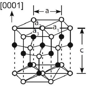
Although zincblende and rocksalt crystal structures are possible in the Group III-Nitride materials system, they predominantly have a wurtzite crystal structure, which is depicted in Figure 2.4. The wurtzite crystal is characterized by two lattice parameters a and c, and comprises alternating close-packed planes of Ga (In or Al) and N atoms in (0001) c-planes, forming an ABAB stacking squence. As a result, the surfaces of the crystals are either of Group III element (Ga-face) or N (N-face) [15]. This polarity brings up very interesting quantum effects that will be discussed later in this thesis.
Figure 2. 3 Wurtzite crystal structure of GaN. Open circles indicate Ga atoms, closed circles show N for Ga-face material. After [16].
III-Nitrides are direct bandgap semiconductors, alloys of which (InxAlyGa1-x-yN,
0≤ x, y, x+y ≤ 1) can be tuned to have bandgap energies spanning a very wide
11
applications ranging from mid-infrared to deep ultraviolet. As we will explain further in the thesis, forming an interface of two semiconductor materials with different bandgap energies, yields a semiconductor heterostructure. Using two or more of such semiconductor heterostructures and placing them very close to each other (by a distance smaller or comparable to the exciton Bohr radius), we can form a quantum well structure and confine electrons and holes in a very close vicinity [17]. Through an increase in electron-hole pair recombination and generation rate, such structures usually help improve the performance of devices that utilize light generation and absorption. Quantum structures based on III-Nitride semiconductors are also very useful for these purposes. In fact, LEDs and LDs that we widely use today comprise such quantum heterostructures, that form the active layers of these devices.
Polarization effects in III-Nitrides
III-Nitride quantum structures have a property that makes them further interesting, which is related with their wurtzite crystal structure. Due to the low degree of symmetry and the aforementioned polarity in their wurtzite crystal structure, there exists a polarization field with two components: spontaneous polarization (Psp) and piezoelectric polarization (Ppz) [18].
Spontaneous component of the polarization field, Psp, exists in wurtzite and other
low crystal symmetry structures and stems from molecular dipoles created by deviations from lattice parameters. Its direction is defined from the metal atom to the nitrogen atom, and thus exists only in c-direction. The spontaneous polarization field intensity is known (theoretically) for GaN, InN and AlN, and therefore can be calculated by simple interpolation for their alloys [18].
Piezoelectric polarization, Ppz, on the other hand, is due to the strain field in the
material. With large differences in lattice parameters, III-Nitrides give rise to strong piezoelectric polarization fields in multilayered structures such as multiple quantum wells (MQW). In fact, the strain in these layers mostly builds up elastically during reactor‟s cooling down, after the growth, due to the differences in thermal expansion coefficients of different layers and the substrate.
12
The direction of Ppz depends on the material being Ga-face or N-face (as Psp) and
the material being under tensile or compressive strain [18]. So, the direction of
Ppz depends on the material below and above, as well. Mathematically, it can be
calculated by multiplying the piezoelectric constant tensor of the material (elements calculated by linear interpolation) and the net strain field on the material. As a general rule, AlGaN on relaxed (or thick) GaN is under tensile strain and Psp and Ppz have the same direction, whereas InGaN on relaxed GaN is
under compressive strain and Psp and Ppz have the opposite direction.
The discontinuity of the net polarization field (P = Psp + Ppz) throughout a
quantum heterostructure causes a sheet charge formation, sign of which depends on the vector difference of the net polarization fields in the two consecutive layers [18]. In multilayer structures including multiple quantum well (MQW) structures, the polarization effect manifests itself as a net built-in electrostatic field, Ewell or Ebarrier, with an alternating direction in well and barrier layers. For a
periodic multiple quantum well structure, the strength of Ewell or Ebarrier, are
described by Equations (2.1) and (2.2) below [18]:
barrier barrier well well well pz well sp barrier pz barrier sp well pz well sp well tot d d P P P P E E E (2.1) well well barrier barrier barrier pz barrier sp well pz well sp barrier pz barrier sp barrier tot d d P P P P E E E (2.2)
Using relevant materials parameters, we can calculate the energy band diagram of such a quantum zig-zag structure as in Figure 2.5.
13
Figure 2. 4 Representative band diagram calculated for an In0.15Ga0.85N/GaN quantum
structure, here the quantum well and barrier thicknesses are 4 nm.
In Equations (2.1) and (2.2), it is assumed that the potential build-up in the MQW structure due to polarization effect is zero [18]. Obviously, that would not be the case when some external electric field is applied to the structure. The external electric field would then be vectorially added to the built-in field in the well and barrier layers. For a typical blue LED with typical quantum well and barrier thicknesses, the built-in electrostatic field inside the quantum well is estimated to be about 300 V/µm, which is a very large, making this effect significant, reducing the probability of electron-hole recombination for light generation [19]. Moreover, for applications requiring larger InN molar ratios in the quantum well layers (to reduce the bandgap of quantum well material) the polarization induced electrostatic field strength in the quantum well layers increases (reducing the electron-hole overlap), since the polarization field is more discontinuous in the interfaces of the quantum wells. This means that polarization effect is more pronounced in green LEDs compared to blue or near UV LEDs. This is one of the main reasons for the lower efficiency of longer wavelength device structures in the III-Nitride optoelectronics.
As mentioned earlier and seen in the Equations (2.1) and (2.2) above, the direction of Ewell or Ebarrier are different. Such electrostatic fields in well and
14
barrier layers with alternating signs, cause MQW structures to have a zig-zag potential profile [19] rather than a square-like one, which is the case for other III-V MQW structures, such as those based on GaAs or InP. This property is one of the main differences between III-Nitrides and other III-V‟s as far as the scope of this thesis is concerned.
Nonpolar and Semipolar III-Nitrides
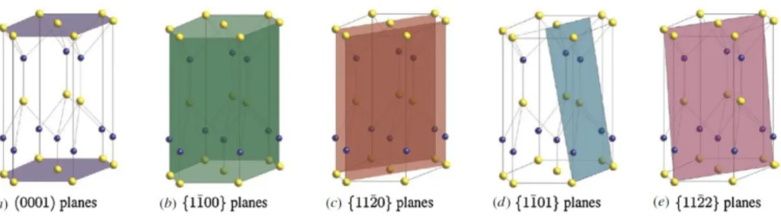
It is very much desirable to achieve polarization-free III-Nitride films, since the electrons and holes would not be separated with the built-in electrostatic fields, and thus excitons would not be ionized in the quantum structures of such films. This is especially important in devices for longer wavelength operation (e.g., green and red) since the polarization induced built-in electrostatic fields are stronger. The growth of such films and structures is possible by changing the growth plane to so-called non-polar planes of wurtzite structure that are perpendicular to the polar c-plane. As indicated in the Figure 2.6 below, a-1120 and m-1100 planes are possible options for non-polar growth of III-Nitrides
[20].
The first attempts to grow GaN on its non-polar planes were not successful and it was impossible to achieve a working device performance due to their low crystal quality [21]. Several substrate materials were studied to achieve high crystal quality non-polar GaN material. In one of the first successful attempts, Craven et.
al. reported device-quality a-plane GaN on r-plane sapphire [22] and a-plane SiC [23]. However, the threading dislocation densities were still high (~1010 cm-2). Among the proposed methods to further reduce the dislocation densities and improving materials quality were growing a thick (~100μm) buffer layer [24], epitaxial lateral overgrowth [22], [25] and using a high temperature nucleation layer [26].
15
Figure 2. 5 (a) Polar, (b) and (c) nonpolar and (d) and (e) semipolar planes of wurtzite GaN crystal structure. Ga atoms are represented by yellow atoms and nitrogen atoms are
represented by blue balls. After [20].
It is also possible to grow GaN on other planes that are in between the polar and non-polar planes, which are called semipolar planes. Two of the most popular semipolar planes are 1101 and 1122 . In these cases, the built-in electrostatic fields are reduced but they are not zero. Some of these planes are given in Figure 2.6.
Although there are additional difficulties on the growth of such materials in their semipolar planes [20], LEDs [27]–[29] and LDs [30] based on semi-polar GaN have been successfully demonstrated. Due to the reduced or eliminated polarization effect in their quantum heterostructures, optoelectronic devices grown on non- and semi-polar planes are of special interest to scientific community and the industry.
2.1.3 Growth of III-Nitrides
Although there are several other methods available for III-Nitride materials growth, such as molecular beam epitaxy (MBE), hydride vapor phase epitaxy (HVPE) and their derivations (e.g., plasma-assisted MBE), metal organic chemical vapor deposition (MOCVD) or metal organic vapor phase epitaxy (MOVPE) is the most popular growth method both in the industry and research, mainly due to its high throughput and good control of growth rates [1]. Regardless the method, c-plane growth is found to be more convenient and thus more studied and better understood compared to nonpolar and semipolar plane growth. Moreover, although there are studies on methods for obtaining free-standing GaN substrates from melt, they have not been as popular as anticipated
16
due to difficulties (requiring pressures up to 10 atm and temperatures up to 1500ºC) as well as small maximum achievable area and cost [31]. As a result, heteroepitaxy (growth on a non-native substrate) has almost become a must. Among the substrates available in the market are sapphire (Al2O3) popular for
III-Nitride based optoelectronic devices (e.g., LEDs and LDs), and silicon carbide (SiC) for electronic devices (high electron mobility transistors) [14]. Using silicon as a substrate material brings a lot of advantages, especially in the cost side, and companies are working towards using silicon instead of Al2O3 and SiC.
In all of our studies, we used sapphire substrates and performed the growth using MOCVD.
MOCVD growth of III-Nitride epitaxy
Chemical vapor deposition (CVD) is a general term used to describe a growth process which involves reaction of molecules in gas form (called precursors) and their decomposition into solid form, usually onto a substrate [32]. It does not imply resultant layer being crystalline, amorphous or polycrystalline. The term metalorganic (or organometallic) refers to the class of compounds used as the precursor material. Each molecule contains a metal atom and organic ligands (e.g., methyl [CH3] or ethyl [C2H6]) attached to it. For III-Nitride MOCVD, the
metalorganic compounds act as the Group III source, whereas ammonia (NH3)
acts as the nitrogen source. The metalorganic compounds used for AlN, InN and GaN and their alloys (AlxInyGa1-x-yN) are trimethylaluminum (TMAl),
trimethylindium (TMIn) and trimethylgallium (TMGa). For the layers that require controlled and low growth rate (especially InGaN/GaN multiple quantum well layers), usually triethylgallium (TEGa) is used instead of TMGa. The basic chemical equation describing the GaN deposition process is as follows:
)
(
3
)
(
)
(
)
(
)
(
CH
3 3v
NH
3v
GaN
s
CH
4v
Ga
(2.3)Although the above chemical reaction seems very simple, the MOCVD growth process is highly complex and hard to understand completely. Toward understanding the MOCVD growth process better, improving it and ultimately
17
achieving superior performing devices, researchers performed empirical studies of important parameters such as growth temperature, pressure, V/III ratio and mass flow rates [32], [33]. As a result of these studies, three different growth regimes were identified. These are, mass transport limited regime, desorption limited regime and surface kinetically limited regime. MOCVD growth of GaN is usually performed in the mass transport limited regime in which growth is limited by the mass transport of the Group III precursor to the growth interface. This regime occurs at a very wide temperature range (600ºC - 1000ºC) and the growth rate usually increases with temperature due to increasing diffusion rate, providing growth rate tunability as well as the ability to grow different alloys that require different growth temperatures [34].
Special care has to be taken for InGaN/GaN layers, in order to obtain optoelectronic devices with good electrical and optical characteristics. This is mainly because high efficiency optoelectronic devices usually require, among other things, high quality quantum well layers with uniform thickness and abrupt interfaces. Moreover, dislocations (which form non-radiative recombination centers and reduce the quantum efficiency) in these layers should be avoided. Another reason for this necessity is because the growth of InGaN layers is difficult compared to GaN. The growth temperature of InGaN layers should be low (<850ºC), due to the low dissociation temperature of InN. Several reports on the observation of In droplets are available in the literature. On the other hand, decomposition of ammonia (NH3) is much less efficient at such low temperatures,
because of the high kinetic barrier for breaking N-H bonds [34]. This tradeoff brings up difficulties for finding a suitable growth window; however, with good growth optimization, it is possible to grow high quality device layers with good reproducibility.
The crystalline quality of the device layers (p- and n-layers and MQWs) also highly depends on the crystalline quality of the layers underneath, especially the buffer layer. Therefore, crystal quality of the buffer layer directly affects the device layers on top of it. The crystalline quality of bulk layers is usually
18
inspected by X-ray diffraction measurements. Generally speaking, the ω-scans of the (002) and (102) reflection rocking curves are narrower for high crystalline quality samples. It was identified that (002) relates to the screw dislocations whereas (102) relates to the edge type dislocations [35], [36].
2.2 Optoelectronic Devices Background
In this chapter, we describe the physics and operation principles of some of the optoelectronic devices with a particular concentration in electroabsorption modulators and light emitting diodes (LEDs). We start from semiconductor device physics, describe some fundamental physical concepts and effects that are especially related with operation and performance of the devices of interest. Building on the semiconductor physics concepts introduced in the earlier parts, we study the optoelectronic devices in more detail. We provide information on the simulation software package that we use for LEDs called APSYS.
2.2.1 Optical processes in semiconductors
In this part, we summarize processes concepts of optical absorption and spontaneous emission, which are related with the operation principles of LEDs, LDs and electroabsorption modulators.
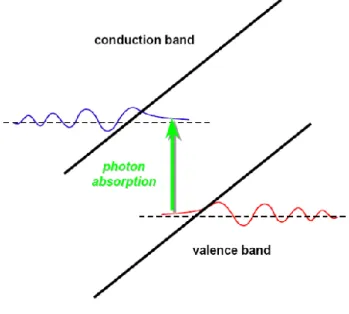
In semiconductors, optical absorption refers to the process of generation of an exciton, bound charge carrier (electron+hole) pair in response to an incident photon. In the case of most semiconductors and devices, electron-hole pair generation occurs by raising an electron from a valence band state to a conduction band state, both of which essentially have the same momentum [37]. The process can be described by Figure 2.7:
19
Figure 2. 6 Interband (band-to-band) absorption (carrier generation) in a semiconductor. An electron in the valence band is raised to another state in the conduction band by a
photon. After [37].
This type of “vertical” transition with momentum conservation describes a direct transition, which is the case for direct bandgap semiconductors like GaAs, GaN, as well as their alloys with other direct semiconductor materials. Moreover, the transition between the conduction and valence bands (rather than within either of the bands) describes an interband (or band-to-band) transition. Here in this thesis, we concentrate on interband transitions in InGaN/GaN quantum structures since the devices we will introduce rely on them. Also, as mentioned earlier, since III-Nitrides are direct bandgap semiconductors, the processes we describe in this thesis work involve direct transitions.
Such transitions might require electron-hole pair generation or recombination. Carrier generation is the process of an electron moving from valence band to the conduction band, with the energy obtained from the absorption of an incoming photon. Electron-hole pair recombination is the opposite of the generation process, and an injected electron is moved from conduction band to valence band and the excess energy is released either as a photon or a phonon emitted from the semiconductor if the process is radiative and as phonon if it is non-radiative. The energy of the emitted photon is determined by the energy difference of initial and final electron states, and either of these states can be an impurity-related luminescent center. InGaN/GaN based LEDs rely on band-to-band transitions; however, impurity-related luminescent center emissions also exist. If the excess energy is transferred to a phonon nonradiatively, it is dissipated as lattice
20
vibrations and converted to heat. Figure 2.8 summarizes some of the most important optical processes in semiconductors that we described above.
Figure 2. 7 Interband (band-to-band) recombination mechanisms. Reproduced after [1].
Band-to-band radiative recombination or stimulated emission is given in process 1 and it is the main mechanism for LEDs. Although radiative recombination through luminescent centers (process 2) is possible in semiconductors, the photons produced by this mechanism do not contribute to useful light for InGaN/GaN LEDs. As mentioned before, nonradiative transitions should be avoided as far as light emitting devices are concerned [1].
There are a few definitions that are helpful for our understanding of optical processes in semiconductors and devices that rely on them. One definition is the internal quantum efficiency, ηint. The internal quantum efficiency is the ratio of
the number of photons emitted inside the semiconductor to the number of carriers that undergo recombination. In other words, it is the probability that a given recombination is radiative [38].
The rates of radiative and nonradiative recombination can be described by inverse of the corresponding lifetimes, τr-1 and τnr-1. Through Fermi‟s golden rule, the rate
of radiative recombination is proportional to the probability of finding an electron and a hole in the same vicinity, which mathematically and quantum mechanically is the squared overlap integral of electron and hole wavefunctions [39]. The total
21 recombination rate τ-1
would be the summation of the two rates. Then internal quantum efficiency, ηint, can be calculated as the ratio of τr-1 andτ-1.
r nr nr r r 1 1 int (2.4)
Obviously, the efficiency of an LED depends on the internal quantum efficiency of the active material used [38]. Therefore, understanding the radiative and nonradiative recombination lifetimes (τr and τnr) is of special importance for our
understanding of optoelectronic devices, especially LEDs.
2.2.2 Electroabsorption in semiconductors
When external electric field is applied to semiconductors, their optical absorption spectra change, this is known as electroabsorption. There are two main mechanisms of electroabsorption: the first one is Franz-Keldysh effect, which is seen in bulk semiconductors, and the other is quantum-confined Stark effect (QCSE), which is seen in quantum structures.
Franz-Keldysh Effect
Franz-Keldysh effect (FKE) [40], [41] appears in bulk semiconductors in which the optical absorption occurs at photon energies equal to or larger than the bandgap of the semiconductor material. When an external electric field is applied across a bulk semiconductor material, the conduction and valence band potential profile become tilted in the energy band diagram. Assisted by an absorbed photon, an excess electron in the valence band can tunnel into the conduction band. In the absence of the external electric field, such transition would not be possible. Another explanation of the same phenomenon is through an eigenstate approach, which is mathematically simpler. Consider an electron in a bulk semiconductor, in the presence of an external electric field in z-direction. The Schrödinger equation then becomes the following:
22 e e c e e e e e z E z z e V z m 2 2 2 (2.5)
The solutions to this equation are the Airy functions, which take the form of oscillatory functions for positions of z where the energy eigenvalue Ec>Ve-eEz
and decaying functions otherwise (within the bandgap) as depicted in Figure 2.9 below.
Figure 2. 8 Schematic representation of Franz Keldysh effect. Courtesy of Prof. David Miller.
The same procedure can be followed for the holes and again eigenfunctions of decaying behavior can be found. It can be predicted through this observation that, application of an external electric field can induce absorption below its bandgap energy, making it absorbing where it is initially transparent. In other words, absorption edge, the wavelength in which the absorption starts, shifts to longer wavelengths (lower photon energies) with the external electric field application. This is especially useful for modulators, by which we can control the absorption level of light. Such devices based on other III-V semiconductors have been thoroughly studied and used in relevant applications [42]–[45].
23
Quantum-confined Stark effect
Similar to Franz-Keldysh effect, quantum-confined Stark effect (QCSE) describes electroabsorption, but this time in quantum structures. In optoelectronics, there are many important and useful outcomes of using quantum structures (e.g., quantum wells, wires or dots) instead of bulk material. Since the carriers are confined in one or more directions, strong excitonic effects can be exhibited. QCSE is one of such strong effects.
In quantum-confined Stark effect, similar to FKE, absorption edge redshifts with the external electric field perpendicular to the quantum well layers [42]. The mechanism is depicted in Figure 2.10 for an infinite quantum well structure.
Figure 2. 9 Electron and hole states in an infinite quantum well with zero external electric field and non-zero electric field. Courtesy of Prof. David Miller.
There are a couple of remarks to consider in this visual description of QCSE: First, electron and hole are pulled in different directions by the electric field and electron and hole wavefunctions overlap less compared to the zero external electric field case. This is an important observation, since the rate of a transition between such states is known to be directly proportional to the squared overlap
24
integral of electron and hole wavefunctions e h 2 through Fermi‟s golden rule
[39]. Moreover, previously forbidden transitions are allowed for the non-zero
external electric field case, since the states are not orthogonal anymore. We will discuss the implications of this observation further in Chapter 5.
As a second remark, the transition energy between electron and hole states is smaller in non-zero external electric field case, indicating a redshift of absorption edge, as in the case of FKE. Representative experimental absorption spectra of an AlGaAs/GaAs multiple quantum well structure at different external electric field levels (perpendicular to the MQW) are given in Figure 2.11.
Figure 2. 10 Optical absorption spectra for AlGaAs/GaAs quantum well structure for various electric fields applied perpendicular across quantum well layers measured at room
temperature. The spectra are shifted vertically to dashed levels for clarity. Courtesy of Prof. David Miller.
It is seen clearly that exciton peaks are shifted to lower energies and become weaker with increasing external electric field. The explanation for that comes from the fact that the electron and hole are separated form each other. As a result, the probability of finding an electron and hole in the same vicinity decreases; and consequently, excitonic absorption decreases.
QCSE has been widely studied and exploited in relevant applications, mostly in GaAs and InP platform [43]–[45] and recently successful demonstrations were
25
made in SiGe platform [46]. All these applications were in the infrared region of the optical spectrum. As we will describe in the next parts, we have demonstrated InGaN/GaN based quantum electroabsorption modulators and studied their underlying physics for better understanding.
Absorption coefficient
Absorption coefficient (denoted as α) is another important physical quantity for our understanding of optical properties of materials, especially semiconductors. In most of the materials, optical absorption can be formally explained as an exponential attenuation of photon flux that passes through the material, characterized by a characteristic absorption coefficient (with units in cm-1). For a device in which photons are absorbed and converted to electron-hole pairs, and electron-hole pairs are collected in the external circuit, such as photodetectors and electroabsorption modulators, the absorption coefficient can simply be related to measurable quantities with the following equation:
R P i d p 1 24 . 1 1 ln 1 0 (2.6)
Here in this equation d is the thickness of the absorbing medium, ip is the
photocurrent, P0 is the optical power in Watts, λ is the wavelength in µm, ζ is the
ratio of electron-hole pairs that successfully contribute to photocurrent and R is the Fresnel power reflectance. By using absorption coefficient, performance and underlying physics of electroabsorption modulators can be studied easily.
2.2.3 LED Model Used
For our LED studies, we used a finite element analysis based simulation package called APSYS (Advanced Physical Models of Semiconductor Devices). APSYS is capable of modeling current-voltage characteristics, and many important parameters such as optical power and spectrum, carrier distributions and band diagrams at various current injection levels. The results deduced from APSYS simulations are very helpful for our understanding of LED operation and possible ways to improve its performance.
26
2.3 III-Nitride Optoelectronic Devices
In this part, we review some of the research work performed in III-Nitride optoelectronic devices field. We start with early work on InGaN/GaN based LEDs and address important achievements, and continue with InGaN/GaN based electroabsorption modulators.
2.3.1 InGaN/GaN based visible LEDs
As mentioned earlier, the first demonstrations of III-Nitride based optoelectronic devices were InGaN/GaN based LEDs, which were demonstrated in early 1990s by Shuji Nakamura of then Nichia Corporation. In the early demonstrations of InGaN/GaN based blue LEDs [1], the forward voltage, Vf, (defined as the voltage
at a driving current of 20 mA) was as high as 10 V and the optical output power level was as low as about 0.125 mW (again, at I=20 mA). A few years after the first demonstrations, the improvements in the device performance were impressive; Vf was reduced down to 3.6 V and the achieved output power levels
were as high as 4 mW [10], [47], [48]. These developments were mainly due to the improvements in the p-doping levels, crystal quality and control on InGaN deposition. Moreover, the latter enabled researchers to extend the operation wavelength range of the LEDs to longer wavelengths, to about 525 nm, which corresponds to green.
Electron blocking layers in LEDs
In the early days of InGaN/GaN based blue LEDs and LDs, a critical improvement in their performance was made through inserting an electron blocking layer (EBL) on top of the multiple quantum well structure, preventing the electron overflow from the active region. The electron overflow in these devices was identified as a major problem because of large electron leakage due to larger diffusion constant of electrons compared to holes, and poor hole injection into the active region due to low hole mobility in III-Nitrides.
27
The EBL is usually composed of p-AlGaN with a typical AlN ratio of 20% and a thickness of 10-20 nm. A representative band diagram (neglecting polarization induced electrostatic fields in MQW) of an InGaN LED with an EBL is shown in Figure 2.12 below.
Figure 2. 11 Band diagrams of two LEDs incorporating (a) an undoped AlGaN EBL and (b) a p-doped AlGaN EBL. After [38].
The Figure 2.12(a) illustrates that the undoped AlGaN EBL acts as a barrier to current flow in both conduction band and valence band. In Figure 2.12(b), valence band edge is smoothed out by the p-doping of the EBL. However, as shown in the inset of the same figure, where the valence band is shown in more detail, there exists a potential spike and notch at the EBL and p-layer interface. It is necessary for holes to tunnel through the potential spike for their injection into the active region and ultimately radiative recombination with electrons. This is an unwanted effect for the incorporation of holes into the active layer. Despite that, today, EBLs are widely used in LEDs and LDs.
28
Efficiency droop in LEDs
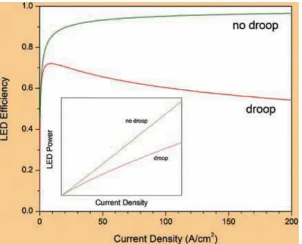
For most applications that LEDs are used such as general lighting, it is necessary to obtain high optical power output levels. In order to achieve high optical power levels, it is necessary to operate LEDs at high current injection levels, another solution would be to increase the number of chips used and/or increase the area of each chip, but those would increase the cost per chip and cost per lumen. For typical sized devices (e.g., 300 μm × 300 μm), the driving currents of more than 350 mA are usually necessary. However, the efficiency of LEDs is the highest at much lower current levels (<50 mA). For larger current levels, the efficiency monotonically decreases. This decrease is called efficiency droop [49]. In Figures 2.13( a) and 2.13(b), we present LED efficiency vs. current and light output vs. current (inset) curves of a typical LED with droop and an LED with no droop. For the typical LED, the LED power deviates from the ideal linear increase with increasing current.
Figure 2. 12 LED efficiency vs. current and LED power vs. current (inset) curves of a typical LED with droop and ideal LED with no droop. After [49].
This problem is known to be stronger in LEDs that operate at longer wavelengths (e.g., green LEDs) and is not related with thermal rollover effect. For that reason it is sometimes referred to as non-thermal rollover. Despite the physical

![Figure 2. 7 Interband (band-to-band) recombination mechanisms. Reproduced after [1].](https://thumb-eu.123doks.com/thumbv2/9libnet/5687058.114710/33.892.261.715.257.519/figure-interband-band-band-recombination-mechanisms-reproduced-after.webp)
![Figure 2. 13 The Schematics illustrating three structures studied in Ref. [56]: (a) the conventional structure with constant AlN molar ratio of 20% (structure A) , (b) the normal](https://thumb-eu.123doks.com/thumbv2/9libnet/5687058.114710/42.892.312.654.635.910/figure-schematics-illustrating-structures-conventional-structure-constant-structure.webp)
![Figure 2. 18 Absorption coefficient change with respect to 0 V absorption curve. After [57]](https://thumb-eu.123doks.com/thumbv2/9libnet/5687058.114710/46.892.293.668.682.985/figure-absorption-coefficient-change-respect-v-absorption-curve.webp)