© TÜBİTAK
doi:10.3906/fiz-1812-3 h t t p : / / j o u r n a l s . t u b i t a k . g o v . t r / p h y s i c s /
Research Article
The effect of phenylboronic acid-based self-assembled monolayers on the
performance of organic field-effect transistors (OFETs)
Tuğbahan YILMAZ ALIÇ1,2,∗,
1Department of Physics, Faculty of Science, Selçuk University, Konya, Turkey 2IMS Laboratory, University of Bordeaux, Bordeaux, France
Received: 04.12.2018 • Accepted/Published Online: 18.03.2019 • Final Version: 08.04.2019
Abstract: The dielectric/semiconductor interface is one of the most important components strongly affecting the per-formance of organic field-effect transistors (OFETs). To improve OFET parameters, we applied a series of phenylboronic acid derivatives as self-assembly molecules between dielectric and organic semiconductor layers. Device performance parameters, especially threshold voltage, current on/off ratio, and subthreshold slope, were improved. To elucidate the mechanism, dielectric/semiconductor interfaces were analyzed using atomic force microscope and contact angle tech-niques.
Key words: Interface modification, self-assembled monolayer, organic field-effect transistor
1. Introduction
The stability and performance of organic field-effect transistors (OFETs) play an important role in optoelectronic applications. Although enormous progress has been made in this research area, many organic electronic applications still require further optimization to fulfill the requirements for improved device performance [1–3]. Modification of the interface between the dielectric and the organic semiconductor (OSC) layers with a self-assembled monolayer (SAM) molecule is a way to improve the electrical characteristics of OFETs. It has been indicated that passivation of the dielectric surface with a SAM molecule can dramatically reduce the density of charge traps at the dielectric/OSC interface and thus ensures an increase in field-effect mobility [3–7]. The effects of passivation of the dielectric surface with a SAM molecule in OFETs have been studied by some researchers for different oxides and SAM molecules [4,5,8]. The improvement of field effect mobility has been attributed to the morphology of OSC induced by the modified surface energy of the SAM-treated dielectric surfaces.
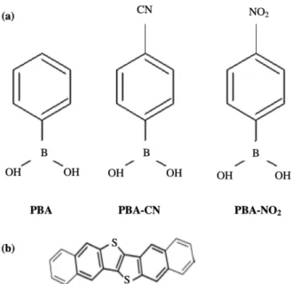
In the present work, we investigated the effect of SAM molecules based on phenylboronic acid derivatives, shown in Figure 1a, on the morphology of the organic active layer and the electrical performances of OFETs. Three different derivatives are described: phenylboronic acid (PBA), (4-cyanophenyl) boronic acid (PBA-CN), and (4-nitrogenedioxidephenyl) boronic acid (PBA-NO2) SAMs. Al2O3 surfaces were treated with
these SAM molecules by dipping in SAM solution for a while. As an active layer, dinaphtho[2,3-b:20,30-f]thieno[3,2-b]thiophene (DNTT) was selected due to its high hole mobility and air stability (Figure 1b) [9,10]. DNTT was deposited by evaporation onto nontreated and treated dielectric surfaces and enhancement in device ∗Correspondence: [email protected]
YILMAZ ALIÇ/Turk J Phys
performance parameters was investigated. The dielectric/semiconductor interfaces were analyzed to determine their morphological properties by AFM and contact angle techniques in order to understand the mechanism behind such an effect.
Figure 1. Chemical structures of (a) SAM molecules and (b) the conjugated organic semiconductor (DNTT).
2. Materials and methods 2.1. Fabrication of OFETs
All OFETs were fabricated on glass substrates using a bottom-gate, top-contact structure as shown in Figure 2b (inset). Aluminum 100 nm thick was deposited as a gate electrode through a shadow mask. The gate dielectric was a thin layer of aluminum oxide of 30 nm thickness obtained by anodization. Surface treatment of the Al2O3
was performed by immersing the films for 24 h at ambient condition in SAM molecules dissolved in isopropanol (IPA) (99.9%, Sigma Aldrich) at 10−3 M concentration. Then 30 nm of DNTT layer as a semiconducting layer was deposited by thermal evaporation at a vacuum base pressure of about 10−6 mbar. The deposition rate was around 0.1 Å/s and the film thickness was monitored using a quartz crystal microbalance. MoO3/Ag source
and drain contacts were deposited by thermal evaporation (thickness 10/60 nm) to achieve a device with a channel length ( L) of 50 µm and a channel width ( W ) of 0.5 mm.
2.2. Characterization
The morphological analyses of SAM-treated and nontreated substrates were performed by contact angle go-niometer (DSA 100 KRÜSS) and atomic force microscope (AFM) (NT-MDT AFM NTEGRA Solaris in ”semi-contact” mode) at room temperature. The electrical characteristics of the fabricated OFETs were carried out in a dry nitrogen glove box at room temperature with a micromanipulator probe station and a 4200 Keithley semiconductor parameter analyzer. Gate voltage dependent mobilities ( µ) were evaluated from linear and sat-uration regimes, and maximum values were given. Threshold voltages ( Vth) were derived from the saturation regime through extrapolation of the linear part of (Ids)1/2.
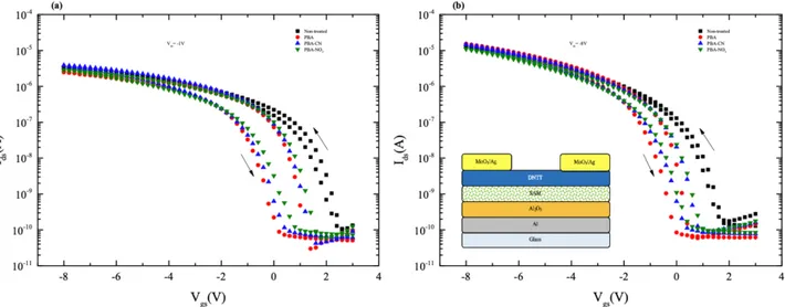
Figure 2. Transfer characteristics in (a) linear regime (Vds = –1 V) (b) saturation regime (Vds = –8 V) of DNTT-based
OFETs with nontreated and SAM-treated Al2O3 insulator at room temperature (inset: structure of devices).
3. Results and discussion
Figures 2a and 2b show the transfer characteristics of the OFET devices based on with and without SAM molecule-treated Al2O3 dielectrics in the linear and saturation regime. The performance parameters of the
OFETs measured after fabrication are summarized in the Table. The effect of SAM molecules on the insulator surface before the semiconductor deposition can be clearly observed in respect to reference devices. In particular, the treatment process increased the Ion/Iof f ratio and decreased the threshold voltage and subthreshold slope (SS) values.
Table. Summary of the OFET parameters obtained from nontreated and treated Al2O3 surfaces with different SAMs. µlin (cm2/Vs) µsat (cm2/Vs) Vth(V) Ion/Iof f SS (V/dec)
Nontreated 0.23± 0.018 0.20± 0.012 0.90± 0.377 6.2 × 10⁴ 0.63
PBA 0.24± 0.022 0.24± 0.007 0.22± 0.128 2.2 × 10⁵ 0.30
PBA-CN 0.26± 0.035 0.26± 0.037 0.49± 0.211 1.8 × 10⁵ 0.37
PBA-NO2 0.21± 0.028 0.21± 0.031 0.63± 0.260 1.1 × 10⁵ 0.47
The transfer characteristics of all OFETs display a small threshold voltage (0.22 to 0.90 V), a large on/off ratio (104–105) , and a subthreshold slope of ~0.3–0.6 V/dec. The field-effect mobilities obtained from
the transfer characteristics of OFETs in both saturation and linear regimes range from 0.20 to 0.26 cm2/Vs.
The mobility of the devices did not show significant differences, indicating that the SAMs probably did not have a prominent impact on the morphology of the organic active layer. However, threshold voltage decreased from 0.9 V in the bare Al2O3 device to 0.2 V in the PBA-treated device, suggesting that the interface
dipole decreased with the addition of SAMs. In general, such an effect also contributes to the reduction of Iof f, consequently leading to the increased Ion/Iof f ratio in SAM-treated devices. SS decreased in SAM devices from 0.63 to 0.3 V/dec, indicating that interface trap densities were minimized following SAM treatment, as SS directly correlates to the capacitance of interface trap densities.
Since electrical parameters of the device appeared to be affected mainly by the surface of the dielectric on which the semiconductor was deposited, the surface energies of various surfaces were compared by contact angle
YILMAZ ALIÇ/Turk J Phys
method. Figure 3 shows the water drop images of nontreated and SAM-treated Al2O3 surfaces. The change in
the measured contact angle values varied from 40°to 73°, clearly evidencing that SAM molecules were anchored on the oxide surface. While PBA and PBA-CN demonstrate slightly more hydrophilic properties compared to bare oxide, PBA-NO2 presents a more hydrophobic character.
Figure 3. Water drop images of nontreated and treated Al2O3 surfaces with different PBA-based SAM molecules.
We further carried out AFM analysis to investigate the effect of SAM molecules on the morphology of the Al2O3 surface. Figure 4 shows AFM surface morphology images of nontreated and treated Al2O3
surfaces. Nontreated surfaces have an average roughness of around 0.3 nm in the scale of 5 × 5 µm. No significant change was observed in average roughness, ranging from 1.0 to 1.3 nm in the scale of 5 × 5 µm after SAM modification. These results showed that the SAMs were anchored successfully onto oxide surfaces in agreement with the contact angle results, despite slightly enhancing the surface roughness. An increase in surface roughness in OFETs generally decreases mobility. On the other hand, lower interface trap density facilitates charge transport. Here these two effects counterbalance each other so that SAM-treated devices do not yield higher mobility values.
4. Conclusions
The effect of SAM molecules based on PBA was investigated. The main transistor parameters were compared to a nontreated bare oxide-based device. Higher current on/off ratios were achieved. Threshold voltages were decreased. These SAM molecules effectively passivated the Al2O3 surface, reducing interfacial trap densities
and consequently lowering subthreshold slopes. Surface analysis using contact angle and atomic force microscopy evidenced SAM grafting on the oxide surface, nonetheless slightly augmenting surface roughness and hindering further mobility enhancement.
Figure 4. AFM images of a) nontreated Al2O3, b) PBA/Al2O3, c) PBA-CN/Al2O3, and d) PBA-NO2/Al2O3
surface in the range of 5 × 5 µm.
Acknowledgments
The author thanks Dr Mahmut Kuş at Selçuk University, Dr Mustafa Can at Katip Çelebi University, and Dr Mamatimin Abbas, Dr Abduleziz Ablat, and Dr Adrica Kyndiah at University of Bordeaux for their support. This study is financially supported by Selçuk University Scientific Research Council (PN: 14101022). The author is also grateful for the financial support from the Scientific and Technological Research Council of Turkey (TÜBİTAK) (2214-A International Doctoral Research Project (PN: 1059B141501270) and 2211-C Priority Areas Domestic Doctoral Scholarship).
References
[1] Horowitz, G. Adv. Polym. Sci. 2010, 223, 113-153. [2] Klauk, H. Chem. Soc. Rev. 2010, 39, 2643-2666.
[3] Ma, H.; Hin-Lap, Y.; Huang, F.; Jen Alex, K. Y. Adv. Func. Mat. 2010, 20, 1371-1388. [4] Casalini, S.; Bortolotti, C. A.; Leonardi, F.; Biscarini, F. Chem. Soc. Rev. 2017, 46, 40-71.
[5] Aghamohammadi, M.; Rödel, R.; Zschieschang, U.; Ocal, C.; Boschker, H.; Weitz, R. T.; Barrena, E.; Klauk, H. ACS Appl. Matet. Inter. 2015, 7, 22775-22785.
YILMAZ ALIÇ/Turk J Phys
[7] Schön, J. H.; Hong, M.; Bao, Z. Adv. Mater. 2002, 14, 323-326.
[8] Onclin, S.; Ravoo, B. J.; Reinhoudt, D. N. Angew. Chem. Int. Ed. 2005, 44, 6282-6304.
[9] Kraft, U.; Takimiya, K.; Kang, M. J.; Rödel, R.; Letzkus, F.; Burghartz, J. N.; Weber, E.; Klauk, H. Organic Electronics 2016, 35, 33-40.
[10] Zschieschang, U.; Ante, F.; Kälblein, D.; Yamamoto, T.; Takimiya, K.; Kuwabara, H.; Ikeda, M.; Sekitani, T.; Someya, T.; Nimoth, J. B. et al. Organic Electronics 2011, 12, 1370-1375.