and Electrical Characterization of Nanoparticles
Can Uran, Emre Unal, Ramazan Kizil, and Hilmi Volkan Demir, Member, IEEE
Abstract—We propose and demonstrate nanowire (NW)
de-vice platforms on-chip integrated using electric-field-assisted self-assembly. This platform integrates from nanoprobes to mi-croprobes, and conveniently allows for on-chip manipulation, cap-turing, and electrical characterization of nanoparticles (NPs). Synthesizing segmented (Au–Ag–Au) NWs and aligning them across predefined microelectrode arrays under ac electric field, we controllably form nanogaps between the self-aligned end (Au) segments by selectively removing the middle (Ag) segments. We precisely control and tune the size of this middle section for nanogap formation in the synthesis process. Using electric field across nanogaps between these nanoprobes, we capture NPs to elec-trically address and probe them at the nanoscale. This approach holds great promise for the construction of single NP devices with electrical nanoprobe contacts.
Index Terms—Dielectrophoresis, electric-field-assisted
self-assembly, nanocrystals (NCs), nanogap, nanoparticle (NP), nanowire (NW).
I. INTRODUCTION
O
NE of the major challenges in nanofabrication commonly arises from the necessity to integrate nanostructures (e.g., nanoparticles, NPs) on the same chip with microcomponents (e.g., microelectrodes) that are orders of magnitude larger in size. For example, in order to make electrical contacts to col-loidally synthesized NPs (typically 1–100 nm in size) by inte-grating them with microelectrodes (typically in the few microm-eters range on the critical side), a very large size mismatch thatManuscript received January 5, 2009; revised February 17, 2009. First published May 27, 2009; current version published October 7, 2009. This work was supported in part by the Turkish National Academy of Sciences Distin-guished Young Scientist Award Program (TUBA GEBIP), in part by the Euro-pean Science Foundation EuroEuro-pean Young Investigator Award (ESF-EURYI), in part by EU under Grant MOON 02139, and in part by TUBITAK under Grant EEEAG 106E020, Grant EEEAG 107E088, Grant EEEAG 107E297, Grant EEEAG 104E114, Grant EEEAG 109E002, Grant EEEAG 105E065, and Grant EEEAG 105E066.
C. Uran is with the Department of Electrical and Electronics Engineer-ing, Nanotechnology Research Center, and Institute of Materials Science and Nanotechnology, Bilkent University, Ankara 06800, Turkey (e-mail: [email protected]).
E. Unal is with the Nanotechnology Research Center and the Institute of Ma-terials Science and Nanotechnology, Bilkent University, Ankara 06800, Turkey (e-mail: [email protected]).
R. Kizil is with the Department of Chemical Engineering, Istanbul Technical University, Istanbul 34469, Turkey (e-mail: [email protected]).
H. V. Demir is with the Department of Electrical and Electronics Engineering and the Department of Physics, Nanotechnology Research Center, and Institute of Materials Science and Nanotechnology, Bilkent University, Ankara 06800, Turkey (e-mail: [email protected]).
Color versions of one or more of the figures in this paper are available online at http://ieeexplore.ieee.org.
Digital Object Identifier 10.1109/JSTQE.2009.2020057
easily ranges from 1:10 to 1:10 000 is required to be handled for successful nano-to-micro integration. This necessitates the ability to manipulate and integrate NPs with a sufficient level of precision on the microchip. In this study, to provide a convenient solution to this challenging problem, we proposed and demon-strated for the first time an on-chip-integrated nanowire (NW) device platform that features controllable nanogap formation in its architecture for capturing and electrical characterization of NPs in the gap, all fully integrated on the same microchip.
Pohl extensively investigated electric field assistance to align and separate various particles, a process also known as dielec-trophoresis (DEP) [1]. Liu et al. previously studied gap forma-tion relying on deposiforma-tion and etching of Ag segment in the middle of Au NWs that are drop-cast on contact pads [2]. In previous work, Au NWs have also been successfully aligned on electrode arrays by using DEP [3]–[5]. Furthermore, metal NP manipulation has been achieved through DEP [6]–[9]. However, to date, there is no research work reported for fabrication and use of electric field-assisted, self-assembled, segmented NWs with controllable-size nanogaps to capture and electrically probe NPs.
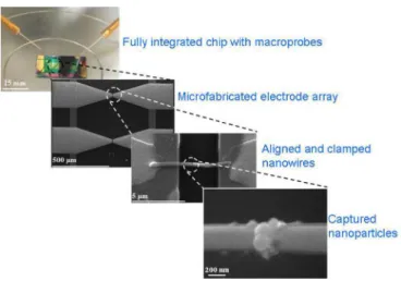
Our approach relies on the use of dielectrophoretic self-assembly of our segmented NWs to construct a nanoscale device platform. One of the key benefits in this approach is that the aligned NWs clamped in the electrodes automatically provide electrical contacts to the captured NPs to allow for electrical probing at the nanoscale. This enables convenient full integra-tion from NPs to NWs to microelectrodes to macroprobes on a single chip, spanning a size range of more than six orders of magnitude (Fig. 1).
II. THEORETICALBACKGROUND
DEP stems from spatially nonuniform electric field distribu-tion, where the induced dipole moment is translated into a net force on polarized particles. This can be used to manipulate particles, also at the nanometer scale. Due to this field gradient, the dielectrophoretic forces are generated as a result of the in-teraction of the applied electrical field with the induced charges, which are not equal on each side of the particles. This inhomo-geneous nature of the electric field distribution causes a nonzero net force. The dielectrophoretic force strongly depends on the oscillation frequency of the applied nonuniform electric field, the complex permittivity of the host medium and the particles, and the particle size.
For example, a spherical particle of radius r with a permit-tivity of εp, in a host medium with the permittivity of εm, the
1414 IEEE JOURNAL OF SELECTED TOPICS IN QUANTUM ELECTRONICS, VOL. 15, NO. 5, SEPTEMBER/OCTOBER 2009
Fig. 1. On-chip-integrated NW device platform that integrates from macro-probes to microelectrodes and to nanomacro-probes for electrical characterization of captured NPs.
dielectrophoretic force is given by
FD EP = 2πr3εmRe [K(ω)]∇Erm s2 (1)
where r is the particle radius, ω is the angular frequency, Erm sis
the root-mean-square electric field, and K(ω) is the Clausius– Mossotti function, which depends on the complex permittivity of the spherical particle and the medium by
K (ω) = ε
∗ p− ε∗m
ε∗p + 2ε∗m (2) where ε∗ = ε− (jσ/ω) is the complex permittivity.
Clausius–Mossotti factor defines the optimum frequency range to use DEP, which is also dependent on the dielectric properties and conductivity of the medium and particles. If the real part of this value is positive, then positive DEP takes place, for which the net force is directed toward the high field gradient and the particles move to high field gradients.
III. FABRICATION
A. Electrode Array Fabrication
We fabricate large arrays of microelectrodes in parallel con-figuration on silicon substrates with different architectural de-signs using standard microfabrication techniques including pho-tolithography, metal deposition, liftoff, and plasma-enhanced chemical vapor deposition (PECVD). On a silicon substrate, we start with depositing silicon oxide (SixOy) of 500 nm in thick-ness with a rate of 28 nm/s at 12 W at 250◦C (or sometimes alternatively, silicon nitride (SixNy) instead of silicon oxide) as the isolation layer using PECVD to decrease the leakage cur-rent, to allow for achieving higher electric field buildup between upper electrodes during dielectrophoretic alignment, and to re-duce noise level during I–V characterization while probing the electrodes. On the top of this dielectric layer, using photolithog-raphy, metal deposition, and liftoff, we define and pattern the first metal layer made of Au (bottom electrodes) that provides an electrical path to upper electrodes by conducting current through ac coupling. This bottom metal layer consists of 20-nm-thick Ti,
Fig. 2. (a) Cross-sectional sketch our device and (b) top view of optical microscopy image of two electrode pairs along with a zoom in of the tips of the upper electrodes.
100-nm-thick Au, and 20-nm-thick Ti. Titanium is used for ad-hesion layer between gold and SixNy. Subsequently, we deposit an adjacent silicon nitride layer of 200 nm in thickness at a rate of 8 nm/s at 12 W at 250◦C. This serves as the dielectric layer for capacitive coupling between the lower electrodes and the upper electrodes. This dielectric layer also prevents electrical shortage of these electrodes to metallic NWs during the assembly process and enables characterization of each NW individually. Finally, we define and pattern the upper gold microelectrodes, which consist of 10-nm-thick Ti and 100-nm-thick Au layers on the silicon nitride layer using the same fabrication techniques as the first layer [Fig. 2 (a) and (b)].
The separation between the tips of our electrode fingers are designed to be 5–6 µm long. The large contact pads and the lower electrodes are designed to achieve the desired level of capacitive coupling between top and bottom metal layers. The large contact pads are set to be 800 µm× 800 µm and the width of the lower electrodes is 60 µm. These parameters are designed to provide reasonable levels of electric field between the fingers of the upper electrodes for field-assisted self-assembly of NWs. For that, the potential drop between the alignment electrodes is maximized increasing the coupling area between the lower and upper electrodes when the voltage is applied to the large contact pads. SixNyis chosen as the intermediate dielectric layer between the two electrodes for its higher dielectric constant of 7.5 compared to that of SixOy, 3.9, which is another factor that increases the potential between the alignment electrodes on the chip.
B. Segmented Nanowire Synthesis
Using electrodeposition, we synthesize Au–Ag–Au seg-mented NWs in porous circular membranes made of alu-minum oxide (Whatman Anodisc) employed as the hard tem-plate [10]–[12]. These membranes are 21 mm in diameter and 60 µm thick with a pore size of 200–300 nm and a pore density of 109cm−2.
First, we deposit silver by chronopotentiometry method with a current level of −1.6 mA for 1200 s from the silver bath (TechniSilver, Italgalvano). This makes sure that the branching portion of the membrane is clogged. The reduction of silver ions occurs for a potential range of−1.40 and −1.70 V for
−1.6 mA of current. Second, we start the deposition of the first
gold segment using a current level of−1.6 mA for 3600 s in the gold bath (Orotemp, Italgalvano). Our rate of gold deposition is 60 nm/min. The reduction of gold ions occurs for a potential range of −1.70 and −2.65 V for −1.6 mA of current. For subsequent Ag segment that determines the size of our gap,
Fig. 3. (a) SEM image of the NWs inside the alumina disc. (b) SEM image of an exemplary NW with a short Ag segment in the middle between long Au segments at the ends (with a total NW length of 7.78 µm).
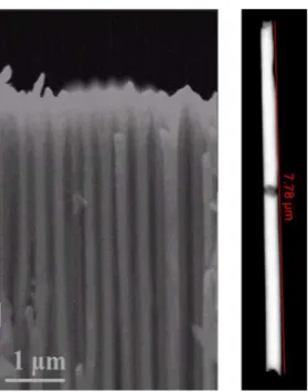
we employ a constant current level of−1.6 mA while varying deposition times to make Ag segments of varying lengths tuned from 300 nm down to 20 nm. Our rate of silver deposition is 85 nm/min. Depending on the deposition time, we produced NWs with size controllable nanogaps. Finally, we deposit Au again applying the same current and deposition time with the first Au segment. The total lengths of the Au–Ag–Au NWs were made to be long enough to bridge the electrodes of our microelectrodes (e.g., 7.2 µm as in our case) [Fig. 3(a) and (b)].
After finishing the electrodeposition, the backside silver layer is etched with nitric acid solution (HNO3 of 30% in
concentra-tion) and alumina disc is dissolved in sodium hydroxide solution (NaOH of 3 M). The NWs remain in this base solution during dissolution. Subsequently, the NWs are centrifuged three times in water at 3000 r/min for 6 min for rinsing, and three times in methanol at 3000 r/min for 6 min, and finally, dispersed in methanol.
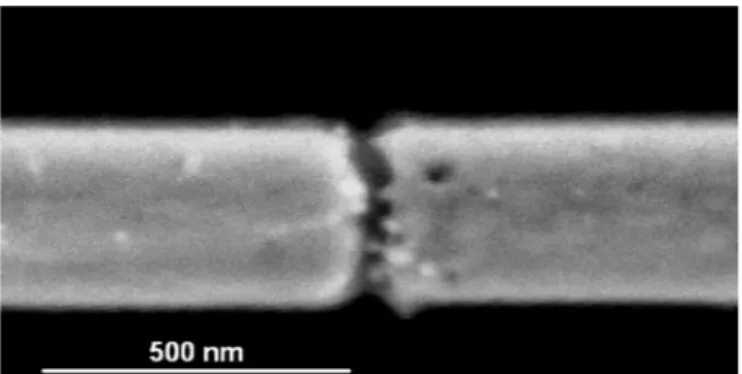
C. Nanogap Formation
After aligning Au–Ag–Au NWs, their middle Ag segments are removed by chemically etching Ag with dilute nitric acid (HNO3) solution and/or by postbaking process at 200◦C for
75 min. This allows for the two ends of the NWs to be automat-ically and precisely aligned. Difficulties in nanogap formation are sometimes encountered due to the high tendency of Au de-position at the walls of alumina pores, forming a meniscus at the frontline of deposition. This adversely affects the morphology of the NW tips, resulting in a curved profile across the radial axis. In addition to chemical etching, baking process is also employed to remove Ag segments, and this is found to help smoothening of our nanogaps. Such thermal baking enables us to form
nar-Fig. 4. Example of Au–Ag–Au segmented NWs with tuned Ag segment lengths of (a) 300 nm, (b) 200 nm, (c) 100 nm, (d) 50 nm, and (e) 20 nm.
rower, uniform gaps, and also strengthens the electrical contacts of the gold segment ends of the NWs to the microelectrodes.
We also characterized gap variation and showed that the length of Ag segment can be precisely controlled by the deposi-tion time. The rate of the silver deposideposi-tion is 85 nm/s. We syn-thesize Au–Ag–Au segmented NWs that include Ag segments with the lengths of 20–50-100–200–300 nm tuned controllably (Fig. 4).
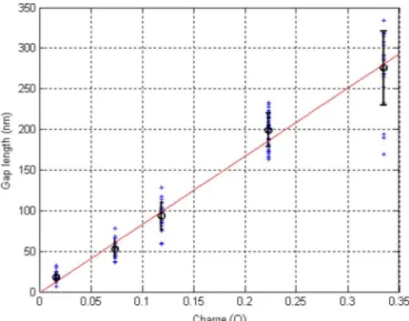
Fig. 5 shows different lengths of Ag segments. The length of these Ag segments is linearly proportional to the total charge injected to the pores of the membrane disc during the electrode-position process. As we drive constant current (I), the injected charge (Q) is also linearly proportional to the deposition time (t) of silver with the simple relation of Q = I× t, which conve-niently allows for controlling the lengths of Ag segments. When Ag segment is selectively chemically etched, we form a nanogap with a size equal to the size of our Ag segment. The deviation among the lengths of Ag segments stems from not being able to drive the same level of current into the pores across the entirety of the alumina disc, and this deviation increases proportionally with deposition time.
1416 IEEE JOURNAL OF SELECTED TOPICS IN QUANTUM ELECTRONICS, VOL. 15, NO. 5, SEPTEMBER/OCTOBER 2009
Fig. 5. Gap length versus injected charge in electrodeposition. (Here plus signs represent the lengths of Ag segments; the circles are the average of these lengths and the error bars are their standard deviation.)
Fig. 6. Nanowire synthesized in track-etched polycarbonate membrane (a) in full view and (b) with a zoom in across its width.
We also synthesized narrow, long NWs, which have diameters of∼40 nm with the ultimate goal of capturing and characterizing single NPs. We synthesized Au–Ag–Au NWs using track-etched polycarbonate membranes (Nuclepore) with pore diameters of 15 nm [Fig. 6(a) and (b)]. It is very demanding to fabricate such NW structures even using e-beam lithography (EBL) and focused ion beam (FIB) technology. This in-membrane NW synthesis is, on the other hand, a highly parallel and cheap process, enabling us to synthesize our NWs in massive numbers.
IV. EXPERIMENTS ANDRESULTS
A. Dielectrophoretic Alignment of Our Nanowires
Using DEP, we align our NWs on the prefabricated micro-electrode arrays with a purpose of single NW alignment across each of the electrode pairs in the array. After dielectrophoretic
Fig. 7. Suspended nanobridge architecture achieved by DEP of the NW on electrodes.
alignment of these NWs on the electrode arrays, we obtain a 3-D suspended bridge architecture with a width of 300 nm by a length of 7200 nm across a pair of electrodes (Fig. 7). It is challenging to fabricate such a suspended structure by standard nanofabrication techniques such as EBL at these di-mensions. EBL provides high resolution (possibly down to 10 nm). It is controllable with high precision. Also, its yield is high in comparison to the DEP alignment process, which is a statistical process. However, EBL is a serial process where a nanostructure is patterned one at a time while DEP is massively parallel.
For our design, we defined some limitation parameters to un-derstand positioning precision. The first one is the translational limit, which is defined by the width of the fingers of our elec-trodes. It describes the position when the NW is aligned parallel across the fingers. In our case, the fabricated finger width is 3 µm. The other one is the rotational limit, which is defined by the length of the aligned NW and the width of a finger. The maximum angle of the aligned NW with respect to fingers is calculated by the ratio of the length of the aligned NW to the width of the relevant finger. In our case, this is 23◦.
In the alignment process, we drop 25–30 µL of the methanol solution containing 7.2-µm-long Au–Ag–Au segmented NWs on our electrode microchip while the signal generator applies an ac bias across the primary pads of our microchip on the corners. Applying the ac signal, the movement of our NWs is monitored in real time through the optical microscope in the probe sta-tion. The drop-casting and alignment steps are repeated two to three times to allow the NWs to flow in the medium without getting stuck on the chip base, and thus get manipulated by dielectrophoretic force across the electrode fingers. For our de-vices on Si/SixOysubstrate, we achieve alignments by applying a sinusoidal wave of Vpp = 50 V across our primary pads for
30–45 s at 10 kHz by observing the chip under the microscope. In the alignment process, our NWs polarize under the applied ac field. As they are more polarizable than the dielectric medium, they align moving toward the electrode fingers as a result of the positive dielectrophoretic force, which is maximized at the high field gradients across the fingers.
The required ac frequency applied for manipulating NWs depends on the dielectric constants and conductivity levels of
of dielectrophoretic force, as the induced charges cannot fol-low the change of polarization with the applied electrical field. For water soluble particles, we apply DEP in water at a differ-ent frequency of 1 MHz, since the dielectric property and the conductivity of the medium substantially changes compared to methanol.
A certain level of potential difference needs to be applied across the main pads to achieve required dielectrophoretic force on NWs. DEP force is directly proportional to the gradient of the square of the electric field (∇E2
rm s). Therefore, in principle,
the resulting DEP force is moving the NWs toward higher field gradient. Thus, ideally, the NWs should be directed to the high-est field gradient where the fingers of the electrodes are located. In reality, however, there are other forces that affect the move-ments of NWs. Brownian motion and thermal effects act against dielectrophoretic manipulation. Moreover, if a NW comes close to or touches the surface, some other short-range strong forces may start to be effective, too. Thus, the dielectrophoretic force must be strong enough to overcome all these other forces for successful manipulation of NWs on to the fingers of the elec-trodes. For Vpp < 50 V, we observed that the resulting
dielec-trophoretic force is not strong enough to form bridges between microelectrodes by aligning NWs. For Vpp > 50 V, undesired
multiple NW alignments are observed to be forming on our mi-croelectrode chips. Therefore, we find the optimal Vpp = 50 V
in our case.
Another important parameter of the alignment process is the NW concentration. Increasing NW concentration also increases the number of single alignments, but this comes at the cost of increased multiple alignments at the same time. Therefore, we use a reasonable NW concentration of 2.5× 10⁷mL−1, which reproducibly achieves high yield alignments more than 20%.
The viscosity of the host medium is also an effective pa-rameter for alignment. Less viscous medium is more useful to manipulate suspending NWs. As we cannot specifically analyze the effect of viscosity in liquids solely as they also have different dielectric constants, we observe the effects of these two proper-ties together. We observe that methanol, which has a viscosity of 0.584 cP at 25◦C and a dielectric constant of 32.6, increases the yield of the alignment compared to isopropanol, which has a viscosity of 1.96 cP at 25◦C and a dielectric constant of 20.18.
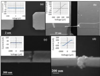
Following the NW alignment, after the field is applied and before the methanol dries over the chip, we clean the chip gently by nitrogen gun to get rid of the unaligned NWs. Additionally, if desired, 20-nm Ti/300-nm-thick Au clamps are patterned on the two sides of the microelectrode arrays to anchor the NWs on the fingers of electrodes (Fig. 8). Also, these clamps facil-itate a better contact between the electrodes and NWs. At this stage, we obtain I–V characterization of the on-chip-integrated NWs (by applying a compliance of 100 nA to prevent the NWs potentially from heating and melting with large current densities).
Fig. 8. SEM images of (a) microelectrode fingers before NW alignment (along with their I –V showing open circuit in the inset), (b) aligned Au–Ag–Au segmented NW by using DEP and clamps (along with its I –V showing electrical
conduction in the inset), (c) NW after gap formation in the middle (along with
its I –V showing open circuit again in the inset), and (d) NPs captured in the size controllable nanogap by using DEP (along with I –V showing electrical
conduction in the inset).
B. Dielectrophoretic Capturing of Nanoparticles
We achieve high electric fields across the etched nanogap be-tween Au segments of the NWs. As a proof-of-concept demon-stration, gold NPs that have a diameter distribution of 80–120 nm in aqueous solution are dropped on the chip where they are ini-tially randomly distributed. Applying a sinusoidal wave with
Vpp of 10 V at 1 MHz across primary pads for 45 s, we
ap-ply electric field between nanogaps formed in the middle of the NWs. Polarized Au NPs are then trapped in these nanogaps where the field gradient and the resulting dielectrophoretic force are large. Finally, after capturing NPs in the gap, we observe strong electrical conduction again across the electrodes.
This approach combines the benefits of using segmented NWs and their alignment using DEP. One of the key benefits in this combined approach is that the aligned NWs automati-cally provide electrical contacts to the captured NPs to allow for their probing and characterization at the nanoscale. Also, since nanogaps are formed with the selective removal of the midsection of the NWs, the two ends of the NWs are auto-matically self-aligned. In the process, before the removal of middle Ag section, we observe electrical conductance through the continuous Au–Ag–Au NW by probing the two connected microelectrodes [shown in the inset of Fig. 8(b)]. However, af-ter the removal of middle section, we observe the open circuit behavior, confirming the formation of a full gap [shown in the inset of Fig. 8(c)].
Finally, after capturing NPs in the gap, we observe strong electrical conduction again across the electrodes. This indicates that metal NPs are captured in the nanogap to bridge and re-tain the conductivity. This implies that our NW arrays with size controllable nanogaps potentially provide a nanoscale device platform convenient for NP capturing and electrical characteri-zation [Fig. 8(d)].
1418 IEEE JOURNAL OF SELECTED TOPICS IN QUANTUM ELECTRONICS, VOL. 15, NO. 5, SEPTEMBER/OCTOBER 2009
Fig. 9. Nanocrystals (20 nm) captured by DEP in 50-nm gap.
Furthermore, with the help of UV illumination at an optical wavelength of 254 nm, we achieve the successful capturing of cadmium selenide/zinc sulfide (CdSe/ZnS) nanocrystals (NCs) in toluene with diameters of∼20 nm (Fig. 9). For this, we ap-ply a sinusoidal wave with a magnitude of Vpp = 10 V between
the primary pads of our chip. Without using UV illumination, we observe no capturing of NCs under the identical experimen-tal conditions. In the previous literature, NCs were captured in 200-nm-wide gaps fabricated by EBL using very high dc biases [13]. In our case, using reasonable ac field, the UV illu-mination increases the polarizability of the NCs, by photogen-erating electron–hole pairs inside them. Increased polarizability directly affects the net DEP force acting on these NCs. This might open up possibilities for the construction of semiconduc-tor NC/nanorod embedded nanoscale devices (e.g. [14]).
V. CONCLUSION
In our study, we proposed and demonstrated constructing an on-chip NW device platform for manipulating, capturing, and electrical characterization of NPs. For this purpose, we syn-thesized Au–Ag–Au segmented NWs and dielectrophoretically aligned them on our microfabricated array of electrodes. After the NWs were aligned, we selectively removed the middle Ag segments, obtaining self-aligned pairs of end Au segments with a nanogap forming between them. Also making a systematic study of the gap size variation, we opened nanogaps of dif-ferent sizes, which can be used for difdif-ferent characterizations and different applications, showing the feasibility of tuning gap formation controllably.
In each step of integration, we made I–V measurements and SEM imaging to show our proof-of-concept demonstration of the NW platform integrated with microelectrodes. In this char-acterization sequence, we first observed an open circuit between the empty microelectrode fingers before NW alignment. Second, a short circuit was obtained when we aligned the Au–Ag–Au segmented NWs on the microelectrodes. Third, an open cir-cuit was achieved between the Au ends of the NWs when we formed nanogaps by removing the middle Ag segments. Fi-nally, a short circuit was accomplished between the Au ends of the NWs after capturing of gold NPs in the nanogaps. This shows that we electrically contacted the NPs trapped in these nanogaps to the NWs and the NWs to the microelectrodes. We
also dielectrophoretically captured NCs. We show that these semiconductor NPs can be captured, enabling their use possibly in optoelectronic nanodevice architectures. The fabrication of such devices is currently underway. Our approach holds great promise for full integration from a single NP to NWs to micro-electrodes to macroprobes on a single chip, possibly enabling such single NP devices.
REFERENCES
[1] M. P. Hughes, “AC electrokinetics: Applications for nanotechnology,”
Nanotechnology, vol. 11, pp. 124–132, 2000.
[2] S. Liu, J. B. H. Tok, and Z. Bao, “Nanowire lithography: Fabricating controllable electrode gaps using Au-Ag-Au wires,” Nano Lett., vol. 5, pp. 1071–1076, 2005.
[3] P. A. Smith, C. D. Nordquist, T. N. Jackson, T. S. Mayer, B. R. Martin, J. Mbindyo, and T. E. Mallouk, “Electric-field assisted assembly and alignment of metallic nanowires,” Appl. Phys. Lett., vol. 77, pp. 1399– 1401, 2000.
[4] J. J. Boote and S. D. Evans, “Dielectrophoretic manipulation and electrical characterization of gold nanowires,” Nanotechnology, vol. 16, pp. 1500– 1505, 2005.
[5] K. H. Bhatt and O. D. Velev, “Control and modeling of the dielec-trophoretic assembly of on-chip nanoparticle wires,” Langmuir, vol. 20, pp. 467–476, 2004.
[6] A. Bezryadin, C. Dekker, and G. Schmid, “Electrostatic trapping of single conducting nanoparticles between nanoelectrodes,” Appl. Phys. Lett., vol. 71, pp. 1273–1275, 1997.
[7] X. Xiong, A. Busnaina, S. Selvarasah, S. Somu, M. Wei, J. Mead, C. L. Chen, J. Aceros, P. Makaram, and M. R. Dokmeci, “Directed assem-bly of gold nanoparticle nanowires and networks for nanodevices,” Appl.
Phys Lett., vol. 91, pp. 063101-1–063101-3, 2007.
[8] N. G. Green and H. Morgan, “Dielectrophoretic separation of nano-particles,” J. Phys. D: Appl. Phys., vol. 30, pp. L41–L44, 1997. [9] B. Razavi, B. R. Martin, T. E. Mallouk, and T. N. Jackson, “Electric
field assisted nanoparticle assembly,” in Proc. Int. Semicond. Device Res.
Symp., 2001, pp. 318–321.
[10] A. Huczko, “Template-based synthesis of nanomaterials,” Appl. Phys. A, vol. 70, pp. 365–376, 2000.
[11] C. Schonenberger, B. M. I. van der Zande, L. G. J. Fokkink, M. Henny, C. Schmid, M. Kruger, A. Bachtold, R. Huber, H. Birk, and U. Staufer, “Template synthesis of nanowires in porous polycarbonate membranes: Electrochemistry and morphology,” J. Phys. Chem. B, vol. 101, pp. 5497– 5505, 1997.
[12] J. J. Mock, S. J. Oldenburg, D. R. Smith, D. A. Schultz, and S. Schultz, “Composite plasmon resonant nanowires,” Nano Lett., vol. 2, pp. 465– 469, 2002.
[13] K. Hoshino, K. Yamada, K. Matsumoto, and I. Shimoyama, “Creating a nano-sized light source by electrostatic trapping of nanoparticles in a nanogap,” J. Micromech. Microeng., vol. 16, pp. 1285–1289, 2006. [14] R. Zhou, H. C. Chang, V. Protasenko, M. Kuno, A. K. Singh, D. Jena, and
H. G. Jing, “CdSe nanowires with illumination-enhanced conductivity: induced dipoles, dielectrophoretic assembly, and field-sensitive emission,”
J. Appl. Phys., vol. 101, pp. 073704-1–073704-9, 2007.
Can Uran received the B.Sc. and M.Sc. degrees in
2006 and 2008, respectively, from the Department of Electrical and Electronics Engineering, Bilkent University, Ankara, Turkey, where he is currently working toward the Ph.D. degree in nanowire device platforms.
Bilkent University, Ankara, where he is engaged in the development of microwave, optoelectronic, and microfluidic devices.
Ramazan Kizil, photograph and biography not available at the time of publication.
Since 2004, he has been working as a Faculty Member at Bilkent University, with joint appoint-ments at the Department of Electrical and Electron-ics Engineering and the Department of PhysElectron-ics. He is the Principal Investigator of the Devices and Sensors Laboratory, and the Associate Director of Nanotechnology Research Center. He also received the Docent title (Associate Professor) in optics and photon-ics from Turkish Council of Higher Education in 2007. His current research interests include the development of nanocrystal/nanowire embedded devices (solid-state lighting devices, photovoltaic devices, modulators, and switches), innovative optoelectronic and RF devices and sensors, and light–matter inter-action at nanoscale. With his students and collaborators, he has authored or coauthored over 100 peer-reviewed research articles in major scientific journals and conferences, presented over 100 invited seminars and talks, and has over ten patents at various stages of the process.
Dr. Demir is the recipient of Parlar Foundation Young Scientist Award (2008), European Science Foundation European Young Investigator (ESF-EURYI) Award (2007), Turkish National Academy of Sciences Distinguished Young Scientist (TUBA-GEBIP) Award (2006), and European Union Marie Curie Fellowship (2005).