Graphene-Based Optical Modulators
Chapter · January 2017 DOI: 10.1142/9789813148758_0013 CITATIONS 0 READS 131 2 authors:Some of the authors of this publication are also working on these related projects:
Single-layer graphene in chemistry and biology: fabrication and applicationsView project Sinan Balci
Izmir Institute of Technology 48PUBLICATIONS 673CITATIONS
SEE PROFILE
Coskun Kocabas
The University of Manchester 138PUBLICATIONS 4,420CITATIONS
SEE PROFILE
All content following this page was uploaded by Sinan Balci on 26 March 2018. The user has requested enhancement of the downloaded file.
435
Chapter 13
Graphene-Based Optical Modulators
Sinan Balci1, and Coskun Kocabas2
1Department of Astronautical Engineering, University of Turkish
Aeronautical Association, 06790 Ankara, Turkey
2Department of Physics, Bilkent University, 06800 Ankara, Turkey
In this chapter, we summarize the recent progress on graphene based optical modulators. Ability to control density of high mobility electrons on large area graphene surface enables realization of new type of electro-optical modulators in optoelectronics. Due to the low electronic density of states, accumulation of charges on graphene significantly shifts the Fermi energy up to 1 eV giving rise to profound optical effects in the infrared and visible spectra. On the other hand, graphene operates as a tunable Drude metal in long wavelengths such as THz and microwave. This unique broadband activity of graphene has stimulated a great deal of interest in graphene community due to its potential use in new optoelectronic devices. After discussing the electrically tunable optical properties of graphene, we highlight the key achievements in the field.
13.1. Introduction
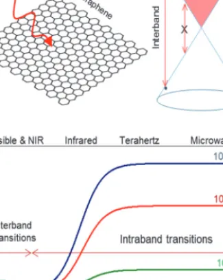
The two-dimensional crystal of carbon, graphene, yields a new platform to control light-matter interaction in a very broad spectrum [1, 2]. Atomic thickness together with the tunable high mobility charge carriers on graphene provides gate-tunable optical properties, which have attracted great interest in the graphene community in order to realize novel optoelectronic devices [3]. Although graphene is one-atom thick, it can yield profound optical absorption due to interband and intraband
Optical Properties of Graphene Downloaded from www.worldscientific.com
electronic transitions. Figure 13.1(a) and 13.1(b) show free standing graphene sheet and its linear band structure. Since the band structure of graphene does not have any energy specific transitions, the optical response of graphene is flat over a very broad spectrum. In the visible and near infrared wavelengths, graphene yields 2.3% optical absorption thanks to the interband transitions between valence and conduction bands [4]. These vertical transitions yield a universal constant optical conductivity of
h
e 2
20
, which yields 2.3% optical absorption in the free standing graphene monolayer. However, on a dielectric substrate, the optical absorption is reduced due the dielectric properties of the environment.Electrostatic gating makes graphene transparent due to Pauli blocking. Doped graphene has a gap in the optical absorption when the photon energy is less than 2EF (EF refers to the shift in Fermi energy from
the Dirac point). Due to unintentional doping and charge puddle formations, pristine graphene has Fermi energy around 0.2 eV which makes graphene transparent for energies less than 0.4 eV. (see Fig.13.1(c))
For longer wavelengths, far-IR, terahertz, and microwave graphene shows metallic like optical response, which can be modeled with Drude like optical conductivity as
σ ω =
ℏ (13.1)where, EF is the Fermi energy, τ is the transport scattering time. Figure
13.1(c) shows the calculated optical absorption of graphene with varying doping levels. As the charge density is varied from 1012 to 1014 cm-2 the
Fermi energy increases from 0.2 to 1 eV resulting in optical transparency in the visible and near IR whereas the absorption of graphene increases up to 50% in THz and microwave regions. These profound activity yields a new platform to control light in a very broad spectrum. This intriguing response originates from the high mobility free electrons on graphene surface. Since the thickness of graphene (~0.3 nm) is much smaller than the wavelength of the incident light (400 nm to 1 m), the optical activity solely originates from the tunable electrons. The lack of bulk material eliminates the
Optical Properties of Graphene Downloaded from www.worldscientific.com
Fig. 13.1. (a,b) Schematic showing of a free standing graphene sheet and its band structure. The interband and intraband electronic transitions are shown on the band structure. Due to Pauli blocking, doped graphene has a gap in the optical absorption. Graphene is transparent for photon energies less than 2EF. (c) Calculated optical absorption of graphene at different doping levels. (τ =200 fs) Graphene is electrically tunable in a very broad spectrum ranging from visible to microwave wavelengths. The activity in the visible is due to Pauli blocking principle. Shifting the Fermi energy blocks the interband transitions and makes graphene transparent for photon energies less than 2EF. For long wavelengths, however, graphene operates as a tunable Drude metal whose response is defined by charge density and transport scattering time.
unnecessary absorption, which gives rise to large unmodulated insertion losses.
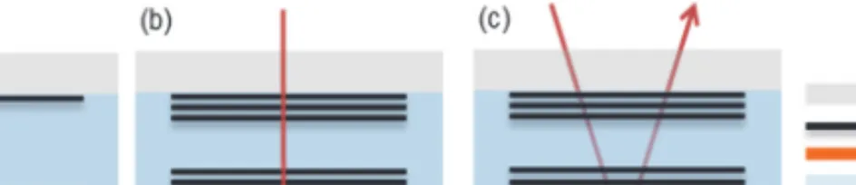
Various electrostatic gating schemes have been developed to control electron density on graphene. Figure 13.2 shows the schematic drawing of the electrostatic gating methods. The most common approach is the back-gating scheme that uses a doped silicon as a back-gate electrode and a thin oxide layer as the gate dielectric. Graphene layer is transferred onto the
Optical Properties of Graphene Downloaded from www.worldscientific.com
oxide surface by using polymer assisted mechanical exfoliation transfer process. In this device configuration, charge densities of 1012 cm-2 and
Fermi energies of 0.3 eV can be easily achieved with large gate voltages (>50 V). However, dielectric breakdown at high gate voltages and common gate electrode are the limiting factors of the back-gating scheme.
Top-gating scheme (Fig. 13.2(b)) is developed to address individual devices on a single chip. A thin dielectric layer is deposited on graphene and followed by a metallization process to define the local gate electrodes. The main advantage of the top-gating scheme is that each device on a single chip can be individually addressable. This is a key requirement for multipixel devices. However, due to hydrophobic nature of graphene surface and incompatible nature of graphene with plasma assisted processes the quality of dielectric films deposited on graphene is very poor. The third approach is the electrolyte gating scheme that uses mobile ions in an electrolyte to gate graphene (Fig. 13.2(c)). Application of a bias voltage between graphene and electrolyte polarizes the ions and forms an electrical double layer (EDL) on the graphene-electrolyte interface. Since the thickness of the EDL is only a few nanometers, the voltage drops rapidly across the EDL and hence leading to a significant electric field that is not possible to obtain by using dielectric based gating schemes (Fig. 13.2(d)). By using this approach, charge density of 1014 and Fermi energy
of 1 eV can be easily achieved. The electrochemical window of the electrolyte is the limiting factor of the achievable charge densities on graphene. Ionic liquids are the most promising electrolyte with large electrochemical window. Alternatively, liquid crystal based proton conducting gel electrolytes have been recently introduced as an electrolyte in graphene optical modulators and graphene Fermi energies of around 1.5 eV has been successfully reached [5].
Based on these gating schemes, rich variety of graphene based optical modulators have been demonstrated [2]. We can classify these modulators into four main categories: (1) waveguide-based modulators, (2) photonic crystal based modulators, (3) supercapacitor-based modulators, and (4) plasmonic based modulators. Although the operation principle of these modulators are the same -Pauli blocking principle- they differ in the way
Optical Properties of Graphene Downloaded from www.worldscientific.com
incident light interacts with graphene layer that defines the interaction path.
Fig. 13.2. (a-c) Common gating schemes used for controlling electronic and optical properties of graphene. (d) Schematic showing of the voltage drop across the gate dielectric and electrolyte based devices. For solid dielectrics, voltage drops linearly between the graphene and gate electrode; however, for liquid electrolytes, voltage drops very rapidly on the interface due the thin electrical double layers which yield very large electric field on graphene.
13.2 Waveguide-based optical modulators
The first class of graphene based electro-optical modulators use a waveguide structure integrated with gated-graphene layer [6-8]. In this configuration, high refractive index waveguide –usually Si- operates as the gate electrode and a thin oxide layer coated on the waveguide serves as the gate dielectric. Graphene is transferred onto the waveguide structure. Figure 12.3(a) shows the first demonstration of the graphene optical modulators operating at the telecommunication wavelengths [7]. The graphene layer on the slot waveguide introduces additional losses due to interband transitions. The evanescent field of the waveguide mode overlaps with the graphene layer. Application of a bias voltage between
Optical Properties of Graphene Downloaded from www.worldscientific.com
the waveguide and the graphene layers shifts the Fermi energy around 0.3 eV, and blocks the
Fig. 13.3. Waveguide based optical modulators. (a) Graphene integrated on a Si slot waveguide. (b) Graphene integrated on a ring resonator. (c) Graphene integrated on a fiber optic waveguide. Figure adapted with permission from: a, ref. 7, b, Ref. [8], and c, Ref. [6], Nature Publishing Group. (For color reference, go to page 497.)
interband transitions at 1550 nm wavelength. The advantage of waveguide configuration is that, the interaction path can be increased with the length of the waveguide. They were able to demonstrate a strong electroabsorption modulation of 0.1 dBµm-1 over a broad range of
wavelengths ranging from 1.35 µm to 1.6 µm [7]. Small footprint of the waveguide structure, 25 µm2, allows switching speed up to 1.2 GHz at 3
dB. Later, different designs including double layer graphene structure have been demonstrated [9]. Very recently Phare et al. implemented the same principle on a ring-shaped optical waveguide with switching speed up to 30 GHz [8]. Figure 12.3(b) shows the schematic drawing of the proposed device structure. Although the switching speed of these devices are promising, the operation wavelength of these modulators are limited to near-IR wavelengths due to limited tunability of the Fermi energy with the back-gating. To overcome this problem, Lee et al. introduced electrolyte gating, which yields Fermi energy shifts up to 0.5 eV [6].
Optical Properties of Graphene Downloaded from www.worldscientific.com
In their optic modulator design, they used a side-polished optical fiber and placed graphene onto the polished side of the optical fiber such that the evanescent field of the fiber can overlap with the graphene layer, Fig. 13.3(c). To achieve high level of doping, they used electrolyte gating. Thanks to the centimeter-long optical path, they were able to show absorption tunability as large as 70%. For the waveguide based optical modulators, there is a tradeoff between switching speed and operation wavelengths. Dielectric based gating provides small footprint with fast switching at IR frequencies (low frequency), whereas electrolyte gating provides slow operation in the visible spectrum (high frequency).
13.2.1 Photonic crystal based optical modulators
The second class of graphene based optical modulators are based on photonic crystals integrated with active graphene layers. The presence of graphene in the photonic crystal cavity introduces additional optical loses that can be controlled via electrical means. Gan et al. demonstrated high-contrast electro-optic modulation of a photonic crystal nanocavity integrated with an electrically gated monolayer graphene [10]. They used ionic gel electrolyte to control Fermi energy of graphene up to 0.8 eV, which yields significant modulation in the quality factor and the resonance wavelength of the cavity. Independently, Majumdar et al. demonstrated a very similar photonic crystal modulator with 60 dB reflectivity modulation [11]. They fabricated a photonic crystal on Si-on-insulator platform with three holes defect. The defect forms the optical nanocavity, which localizes the light inside the photonic crystal. After coating the surface of the cavity with graphene, the quality factor of the cavity is drastically reduced from 1500 to down to 500 due to additional optical losses. They observed narrowing in the cavity line width and an increase in the cavity reflectivity with increasing charge density on graphene. Both designs provide an electrically tunable photonic cavity operating in near-IR wavelengths. The physical footprint for the graphene-photonic crystal cavity (~a few µm2) is significantly reduced when compared with
graphene-waveguide optical modulator footprint (~25 µm2). Very
recently, Gao et al. demonstrated high speed photonic crystal modulator using graphene-boron-nitride heterostructure integrated with the photonic
Optical Properties of Graphene Downloaded from www.worldscientific.com
nanocavity [12]. Sandwiching graphene between two monalayer-BN layers, which operate as gate
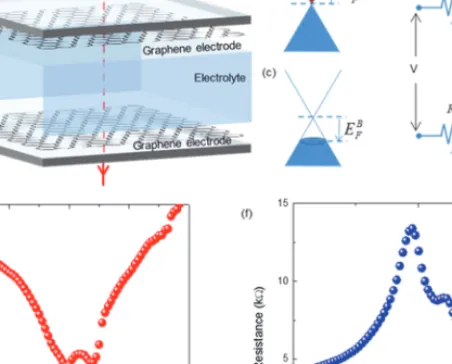
Fig. 13.4. Graphene supercapacitor operates as an optical modulator. (a) Schematic drawing of a parallel plate graphene supercapacitor formed by two large area graphene electrodes and electrolyte medium in between. (b,c) Band structure of graphene electrodes under a voltage bias. (d) Small signal circuit model of the device. (e,f) Variation of the resistance and capacitance of the device. Figure adapted with permission from: Ref. [14], American Chemical Society.
dielectric, yields very high mobility graphene due to the lower number of charged impurities on the substrate. The improvement of the quality of graphene yields a significant enhancement in the switching speed and reduction in the operation voltage. These initial works provide the foundation of graphene based electrically tunable integrated optical components that could yield more complex photonic integrated circuits.
Optical Properties of Graphene Downloaded from www.worldscientific.com
13.2.2 Graphene supercapacitor based optical modulators
One unique advantage of graphene over other conventional 2D electronic systems (such as Si inversion layer and GaAs heterostructures) is that it can be grown over very large area [13]. Combining electrical tunability with the large area growth yields new perspective for large area electrically reconfigurable devices. Polat et al demonstrated a large area optical
Fig. 13.5. (a) Variation of the optical transmittance spectra of graphene supercapacitor at different bias voltages. (b) The extracted Fermi energy and total capacitance of the device. Figure adapted with permission from: Ref. [14], American Chemical Society. (For color reference, go to page 497.)
modulators using graphene supercapacitor, which is a good example for graphene enabled devices [14]. Figure 13.4(a) shows their design which includes a parallel plate graphene supercapacitor filled with a liquid electrolyte. Two large area graphene electrodes are transferred onto optically transparent quartz substrates. Electrolyte is injected between the graphene electrodes. This device structure provides self-gating mechanism between the graphene electrodes without requirement of a metallic gate electrodes. Under a bias voltage, the electrolyte gets polarized and forms electrical double layers at the graphene-electrolyte interface. Since the electrical double layer is very thin, the accumulated ions yield very large electric field and increase the carrier concentration on the graphene electrodes. Holes and electrons accumulate on opposite electrodes. Figure 13.4(b) and 13.4(c) show the band structure of graphene electrodes under a bias voltage. In this design, the graphene electrodes have double role,
Optical Properties of Graphene Downloaded from www.worldscientific.com
they operate as (i) the conductive electrode and (ii) the active layer. As the charges accumulate on the electrodes, the Fermi energy shifts to higher energies resulting in variation of resistance and quantum capacitance of the electrodes. The small signal model of the device is shown in Fig. 13.4(d), where the graphene electrodes are modeled with a variable resistor and a capacitor and the electrolyte is modeled by a capacitor representing the double layer capacitance. Since the electrostatic capacitance of the double layers is much larger than the quantum capacitance of the
Fig. 13.6. Various modulator designs to improve the optical modulation. Figure adapted with permission from: ref. 14, American Chemical Society.
electrodes, total capacitance is limited by the quantum capacitance. The Fermi energy of the graphene defines the resistance (R) and quantum capacitance (CQ) of the electrodes. Since the density of states of the atomic
electrodes are very small, accumulation of charges results in large shifts of Fermi energy. Figure 13.4(e) and 13.4(f) show the variation of the total capacitance and resistance of the device. At charge neutrality point, the capacitance shows a minima and resistance reaches to a maxima. Two distinct maxima and minima are due to the differences between the Dirac point of the top and bottom electrodes.
Figure 13.5(a) shows the modulation of the transmittance at different bias voltages. Due to Pauli blocking, graphene becomes transparent to energies less than 2EF. The transmittance spectra shows a step-like
function with cutoff energy at 2EF.
Fermi energy of the graphene electrodes can be extracted from the transmittance spectra. Figure 13.5(b) shows the variation of the Fermi energy with bias voltages and its comparison with the capacitance of the
Optical Properties of Graphene Downloaded from www.worldscientific.com
device which scales similarly with the charge density. The performance of the device is limited with the optical absorption of the graphene electrodes. Figure 13.6 shows various device configurations to improve the modulation depth of the graphene supercapacitor.
13.2.3 Graphene based electrochromic devices
Replacing single layer graphene with multilayer graphene in the supercapacitor modulators provides new perspective for optical modulators and electrochromic devices. Besides broad optical activity,
Fig. 13.7. (a) Schematic drawing of multilayer graphene based flexible electrochromic devices. (b) Optical transmittance of the device at different bias voltages. (c,d) Photograph of the device at 0 and 5 V bias voltage. Figure adapted with permission from: Ref. [15], Nature Publishing Group.
thickness of graphene enables fabrication of these devices on flexible substrates. Using CVD grown multilayer graphene, Polat et. al demonstrated new types of flexible electrochromic devices on polymer substrates [15]. Figure 13.7 depicts the schematic drawing of the flexible electrochromic device using multilayer graphene as an optically active layer. Multilayer graphene (MLG) simultaneously offers all key
Optical Properties of Graphene Downloaded from www.worldscientific.com
requirements for practical applications; high-contrast optical modulation over a broad spectrum, good electrical conductivity, and mechanical flexibility. This method relies on electro-modulation of interband transition of MLG via intercalation of ions into the graphene layers which yields significant modulation in optical transmittance.
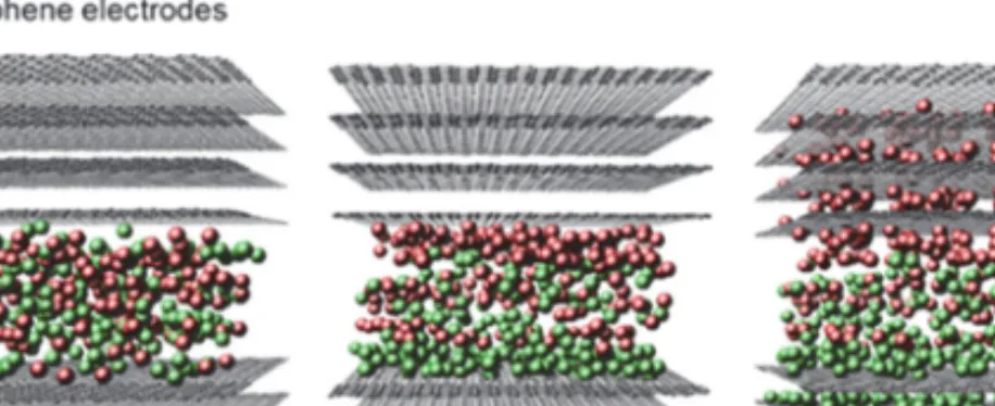
Figure 13.8 shows the proposed mechanism for controlling optical properties of multilayer graphene supercapacitor. In single layer graphene case, formation of ionic double layer at graphene-electrolyte interface is sufficient to control doping on graphene electrodes. However, for multilayer graphene electrodes, accumulation of ions can only dopes first
Fig. 13.8. Electrostatic doping of multilayer graphene via intercalation process. Unlike single layer graphene, formation of electrical double layer is not enough to gate the underneath layers due to screening. At large bias voltages, ions intercalate multilayer graphene which results in efficient gating of Fermi energies up to 1.5 eV. Figure adapted with permission from: Ref. [15], Nature Publishing Group. (For color reference, go to page 498.)
a few layers due to the electrostatic screening of the underneath layers. However, during ion intercalation process, ions can penetrate into thick film up to 100 graphene layers that yields optical modulation of 60% in the visible and near IR wavelengths, Fig. 13.9. There is a tradeoff between the modulation depth and thickness of the graphene film. As the thickness of the film increases, the modulation depth increases, however for very
Optical Properties of Graphene Downloaded from www.worldscientific.com
thick samples, the efficiency of intercalation process decreases and leads to less smaller
Fig. 13.9. Modulation of optical transmittance of multilayer graphene with varying multilayer graphene thicknesses. Figure adapted with permission from: ref. 15, Nature Publishing Group.
modulation and large insertion losses. Polat et al also demonstrated a reflection type electrochromic devices by replacing one graphene electrode with a reflecting gold electrode [15]. Furthermore, multi pixel display devices using pattered multilayer graphene has been demonstrated on flexible polymer substrates [15].
13.2.4 Plasmonics based graphene optical modulators
The third class of graphene based optical modulators is based on plasmonic based optical modulators where metallic nanostructures have been elegantly combined with single graphene layer [16-18]. Metallic nanostructures support surface plasmon polaritons (SPPs), which can concentrate incident light into a deep subwavelength volume, and thus SPPs lead to variety of appealing fundamental and practical applications such as spectroscopy, biosensing, nanophotonics, nanoelectronics, and solar cells [19]. To boost the performance of plasmonic devices at the nanoscale dimension and to enlarge the applicability of plasmonic nanostructures active control of the SPPs is always desirable and thus a large amount of efforts has been recently dedicated in this direction to actively control plasmon resonance in the visible and infrared part of the electromagnetic spectrum [20, 21]. Graphene provides a unique
Optical Properties of Graphene Downloaded from www.worldscientific.com
opportunity to modulate plasmon resonance at optical frequencies due to the presence of electrically controllable electronic interband transitions in graphene and the tunability of graphene conductivity by electronic gating as well. In addition, graphene can be easily integrated into the plasmonic nanostructures such as flat metal thin films, and metallic nanoparticles because of flexible nature of graphene sheets and graphene’s compatibility with the nanofabrication processes. For example, Salihoglu et al placed graphene onto silver and gold surfaces and investigated SPPs on graphene-metal surfaces [22]. Ansel et al. fabricated and studied hybrid graphene plasmonic waveguide optical modulator, Fig. 13.10(a) [17]. The non-transparent grating on a gold surface couples incident light into SPPs, on the other hand, the transparent grating located at the other end of the device then decouples SPPs into light. The gated graphene placed on top of a boron
Optical Properties of Graphene Downloaded from www.worldscientific.com
Fig. 13.10. Principles of plasmonic based optical modulators. (a) Hybrid plasmonic waveguide optic modulator. Uniform non-transparent grating couples incident light into SPPs which are modulated by graphene located on top of the dielectric spacer layer. Uniform transparent grating, on the other hand, decouples SPPs into light. (b) Graphene-gold nanowire hybrid nanostructure on a glass substrate. An electrolyte is used to control optical interband optical transitions in graphene. (c) Graphene-Ag nanoprism hybrid nanostructure placed on a glass substrate. The separation between graphene and Ag NPs are controlled with a spacer dielectric layer grown by ALD. Energy transfers from Ag NPs to graphene where graphene and Ag NPs behave as energy acceptors and donors, respectively. Figure adapted with permission from: a, Ref. [17], Nature Publishing Group, b, Ref. [16], American Chemical Society, and c, ref. 18, Optical Society of America. (For color reference, go to page 498.)
nitride flake affects SPPs propagation on the gold surface. In this way, the optical plasmonic modulator working at the telecom range was
Optical Properties of Graphene Downloaded from www.worldscientific.com
demonstrated. Furthermore, the demonstrated optical modulator had a modulation depth of >0.03dBµm-1 at low gating voltages. Graphene
interaction with light has been greatly increased by fabricating a simple coplanar graphene configuration that involves SPPs propagation along a metal-dielectric interface adjacent to a graphene layer. At normal light incidence, graphene has relatively small absorption of 2.3% defined by the fine structure constant [4]. When light is incident on and transmitted through a graphene layer, the interaction between graphene and incident light has been enormously increased. Therefore, in this coplanar configuration a modulation depth of around 0.1 dB per graphene layer can be achieved.
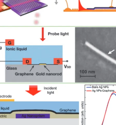
In an another type of device structure, Kim et al demonstrated electrical controlled plasmonic resonance at infrared using gold nanorod-graphene hybrid nanostructure [16]. The principle of the plasmonic based optical modulator is shown in Fig. 13.10(b). It should be notified here that, in this study, the hybrid graphene-gold nanostructure was probed at the single-nanoparticle level using dark-field Rayleigh scattering spectroscopy of individual gold nanorods. Both the plasmon resonance and quality factor of gold nanorod plasmon is efficiently modulated. The results reveal that plasmon-graphene coupling is remarkably strong and they claim that even a single electron resting in graphene could affect the plasmon resonance in gold nanowire. Electrically tunable interband transitions in graphene at optical frequencies enable electrical modulation of plasmon resonance. For electrical gating of graphene a top electrolyte gating with an ionic liquid was used.
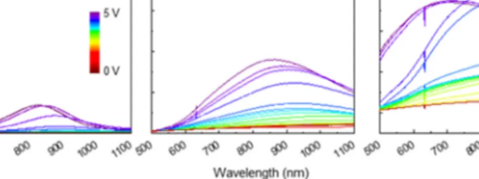
Recently, in the visible spectrum, Balci et al have actively modulated plasmon resonance of silver nanoprisms (Ag NPs) in graphene-Ag NPs hybrid nanostructure, Fig. 13.10(c) [18]. Ag NPs have tunable plasmon resonances ranging from 400 nm to 1100 nm and they can be uniformly coated on glass or silicon substrates [23]. The fabricated structure was in large area and the optical measurements were performed at the ensemble level. The interband transitions in graphene at optical frequencies can be easily controlled by ionic liquid top gating of graphene. As a result, the Fermi energy level of graphene can be tuned from around 0.2 eV to 1.2 eV which enables efficient control of graphene absorption in the visible spectrum because of the Pauli blocking. Both plasmon resonance
Optical Properties of Graphene Downloaded from www.worldscientific.com
Fig. 13.11. Modulating plasmon resonance with graphene in the visible spectrum. (a) Optical transmission of the hybrid device for various applied bias voltages. (b) Plasmon resonance frequency (wavelength) increases (decreases) with the applied bias voltages. (c) Quality factor of the plasmon resonance at around 800 nm is significantly increased with the increase in the applied bias voltages. At low voltages, graphene induced loss in the medium is large due to the interband transitions in the graphene in the visible spectrum. At high voltages, the interband transitions are blocked and thus quality factor of the plasmon increases. Figure adapted with permission from: Ref. [18], Optical Society of America.
frequency and quality factor have been reversibly modulated by 20 and 35 meV, respectively. The separation between graphene and Ag NPs were controlled at the atomic scale by using atomic layer deposition (ALD) technique. The results indicate that the coupling between graphene and Ag NPs strongly depends on the dielectric layer thickness between them. Transmission spectra of the graphene-Ag NPs structure as a function of the applied bias voltage demonstrate that plasmon resonance of the Ag NPs can be electrically tunable, Fig. 13.11. The experimental results obtained in this work was explained by a damped harmonic oscillator (DHO) model [18]. In this model, a plasmon is considered as a damped harmonic oscillator in which an electron having a mass m attached to a spring having a spring constant k oscillates with a natural frequency f = (k/m)1/2/2п. If there is a damping force represented as F
damping = -bv where
b and v are damping constant and velocity of oscillating object here an
electron, respectively. Under damping condition, fdamped =
(k/m-(b2/4m2))1/2/2п = (f2-γ2)1/2 where γ is the total damping rate. It is obvious
here that under the damping condition, both the magnitude of the plasmon
Optical Properties of Graphene Downloaded from www.worldscientific.com
frequency and the quality factor of the plasmon resonance decrease. The DHO model successfully explains the observed modification in plasmon resonance as a function of the applied bias, Figure 13.11. At high bias voltages, the interband transitions in graphene are totally blocked and thus the loss in the medium because of the presence of graphene layer is blocked out and hence plasmon resonance frequency is shifted to high frequency. At low bias voltages, the interband transitions in graphene are not blocked out and the loss in the medium is large and thus plasmon resonance frequency is now at low frequency.
13.2.5 Graphene-based long wavelength optical modulators
In the previous sections, we summarize the graphene based optical modulators operating in the visible and near IR wavelengths. The operation principle of all of these devices are based on Pauli blocking principle that yields around 2.3% modulation per graphene layer. We now turn our attention to long wavelengths, i.e. terahertz and microwave. However, at long wavelengths, graphene operates as a tunable Drude metal, which yields much larger activity. The mechanism behind this large tunability is the intraband transitions whose rate is controlled by Fermi level and the associated density of charge carriers on the graphene. The activity in long wavelength makes graphene a unique material for active THz and microwave devices [24, 25]. The main challenge for long wavelength photonic devices is the physical dimensions of the device defined by the wavelength. For example, for an active microwave device operating at a frequency of 10 GHz (wavelength of 3 cm), the device dimension should be larger than 10 cm [26]. The conventional high mobility semiconducting materials are not suitable for large scale applications. High mobility of graphene, together with the ability to be synthesized over large areas, opens new opportunities for active long wavelength devices. Figure 13.12 summarizes some recent achievements in graphene enabled long wavelength active devices including switchable radar absorbing surfaces [25] and THz spatial light modulators [24]. Figure 13.12(a) shows an active microwave surface fabricated by graphene supercapacitors. Two very large area graphene sheets were synthesized by chemical vapor deposition and transferred on microwave
Optical Properties of Graphene Downloaded from www.worldscientific.com
transparent polymer substrates. Under a bias voltage, high mobility electrons accumulate on graphene electrodes and control the microwave
Fig. 13.12. Graphene enabled large scale active devices operating in THz and microwave frequencies. (a) Active microwave surface. (b) Multipixel spatial THz modulator. (c) Switchable radar absorbing surfaces. (d,e) Nonplanar active microwave surfaces. Figure adapted with permission from: a, c and d from Ref. [25], Nature Publishing Group. And b, from Ref. [24] Optical Society of America. (For color reference, go to page 499.)
Optical Properties of Graphene Downloaded from www.worldscientific.com
reflectivity and transmittance of the surface. This device is a microwave analog of smart windows whose transmittance is modulated by electrical means. Combining these active microwave surfaces with different device designs enables electrically switchable radar absorbing surfaces with more than 50dB switchable suppression ratio. Kakenov et al. implemented similar device concept to control THz waves [26]. They were able to control THz transmittance through graphene capacitor with moderate bias voltages. They extended their work by integrated arrays of graphene device to form a spatial THz modulator (Fig. 13.12(b)) [24].
13.3. Conclusions
In conclusion, graphene provides a tunable optical platform to control light-matter interaction in a very broad spectrum ranging from visible to microwave frequencies. This profound tunability originates from high mobility free carriers on graphene surface whose density can be controlled by various gating schemes. Rich variety of active optoelectronic devices has been demonstrated. In this chapter, we summarize the recent progress on graphene based optical modulators fabricated by active graphene layer integrated on waveguides, photonic crystals, and plasmonic structures. In addition to the optoelectronic devices operating in the visible and infrared, there are recent examples for long wavelength modulators, which could find immediate applications, for example, in radar absorbing surfaces and THz communications.
Acknowledgements
Coskun Kocabas acknowledges the partial funding from TUBİTAK (The Scientific and Technological Research Council of Turkey) under the Project No. 113F278 and 114F052. He also acknowledges the support from the European Research Council (ERC) Consolidator Grant ERC – 682723 SmartGraphene.
Optical Properties of Graphene Downloaded from www.worldscientific.com
References
[1] Novoselov, K.S., et al., Electric field effect in atomically thin
carbon films. Science, 2004. 306(5696): p. 666-669.
[2] Sun, Z., A. Martinez, and F. Wang, Optical modulators with 2D
layered materials. Nat Photon, 2016. 10(4): p. 227-238.
[3] Bonaccorso, F., et al., Graphene photonics and optoelectronics. Nature Photonics, 2010. 4(9): p. 611-622.
[4] Nair, R.R., et al., Fine structure constant defines visual
transparency of graphene. Science, 2008. 320(5881): p.
1308-1308.
[5] Tunkara, E., et al., Highly Proton Conductive Phosphoric
Acid-Nonionic Surfactant Lyotropic Liquid Crystalline Mesophases and Application in Graphene Optical Modulators. Acs Nano,
2014. 8(10): p. 11007-11012.
[6] Lee, E.J., et al., Active control of all-fibre graphene devices with
electrical gating. Nature Communications, 2015. 6.
[7] Liu, M., et al., A graphene-based broadband optical modulator. Nature, 2011. 474(7349): p. 64-67.
[8] Phare, C.T., et al., Graphene electro-optic modulator with 30 GHz
bandwidth. Nature Photonics, 2015. 9(8): p. 511-+.
[9] Liu, M., X.B. Yin, and X. Zhang, Double-Layer Graphene
Optical Modulator. Nano Letters, 2012. 12(3): p. 1482-1485.
[10] Gan, X.T., et al., High-Contrast Electrooptic Modulation of a
Photonic Crystal Nanocavity by Electrical Gating of Graphene.
Nano Letters, 2013. 13(2): p. 691-696.
[11] Majumdar, A., et al., Electrical Control of Silicon Photonic
Crystal Cavity by Graphene. Nano Letters, 2013. 13(2): p.
515-518.
Optical Properties of Graphene Downloaded from www.worldscientific.com
[12] Gao, Y.D., et al., High-Speed Electro-Optic Modulator Integrated
with Graphene-Boron Nitride Heterostructure and Photonic Crystal Nanocavity. Nano Letters, 2015. 15(3): p. 2001-2005.
[13] Polat, E.O., et al., Synthesis of Large Area Graphene for High
Performance in Flexible Optoelectronic Devices. Scientific
Reports, 2015. 5.
[14] Polat, E.O. and C. Kocabas, Broadband Optical Modulators
Based on Graphene Supercapacitors. Nano Letters, 2013. 13(12):
p. 5851-5857.
[15] Polat, E.O., O. Balci, and C. Kocabas, Graphene based flexible
electrochromic devices. Scientific Reports, 2014. 4.
[16] Kim, J., et al., Electrical Control of Optical Plasmon Resonance
with Graphene. Nano Letters, 2012. 12(11): p. 5598-5602.
[17] Ansell, D., et al., Hybrid graphene plasmonic waveguide
modulators. Nature Communications, 2015. 6.
[18] Balci, S., et al., Dynamic tuning of plasmon resonance in the
visible using graphene. Optics Letters, 2016. 41(6): p. 1241-1244.
[19] Ebbesen, T.W., et al., Extraordinary optical transmission through
sub-wavelength hole arrays. Nature, 1998. 391(6668): p. 667-669.
[20] Pala, R.A., et al., A nonvolatile plasmonic switch employing
photochromic molecules. Nano Letters, 2008. 8(5): p. 1506-1510.
[21] Sterl, F., et al., Magnesium as Novel Material for Active
Plasmonics in the Visible Wavelength Range. Nano Letters, 2015.
15(12): p. 7949-7955.
[22] Salihoglu, O., S. Balci, and C. Kocabas, Plasmon-polaritons on
graphene-metal surface and their use in biosensors. Applied
Physics Letters, 2012. 100(21).
[23] Balci, S., Ultrastrong plasmon-exciton coupling in metal nanoprisms with J-aggregates. Optics Letters, 2013. 38(21): p.
4498-4501.
[24] Kakenov, N., et al., Graphene-enabled electrically controlled
terahertz spatial light modulators. Optics Letters, 2015. 40(9): p.
1984-1987.
[25] Balci, O., et al., Graphene-enabled electrically switchable
radar-absorbing surfaces. Nature Communications, 2015. 6.
[26] Kakenov, N., et al., Broadband terahertz modulators using
self-gated graphene capacitors. Journal of the Optical Society of
America B-Optical Physics, 2015. 32(9): p. 1861-1866.
Optical Properties of Graphene Downloaded from www.worldscientific.com
by CHINESE UNIVERSITY OF HONG KONG on 02/28/17. For personal use only.
View publication stats View publication stats