An Efficient Computation Model for Coarse Grained Reconfigurable Architectures
and its Applications to a Reconfigurable Computer
Oguzhan Atak and Abdullah Atalar
Department of Electrical and Electronics Engineering Bilkent University, Ankara, Turkey
{atak,atalar}@ee.bilkent.edu.tr
Abstract—The mapping of high level applications onto the
coarse grained reconfigurable architectures (CGRA) are usu-ally performed manuusu-ally by using graphical tools or when automatic compilation is used, some restrictions are imposed to the high level code. Since high level applications do not contain parallelism explicitly, mapping the application directly to CGRA is very difficult. In this paper, we present a middle level Language for Reconfigurable Computing (LRC). LRC is similar to assembly languages of microprocessors, with the difference that parallelism can be coded in LRC. LRC is an efficient language for describing control data flow graphs. Several applications such as FIR, multirate, multichannel filtering, FFT, 2D-IDCT, Viterbi decoding, UMTS and CCSDC turbo decoding, Wimax LDPC decoding are coded in LRC and mapped to the Bilkent Reconfigurable Computer with a performance (in terms of cycle count) close to that of ASIC implementations. The applicability of the computation model to a CGRA having low cost interconnection network has been validated by using placement and routing algorithms.
Keywords-Coarse Grained Reconfigurable Architectures I. INTRODUCTION
Reconfigurable computing has evolved from Field Pro-grammable Gate Array (FPGA) architectures. FPGA im-plementation of many applications have been shown to be efficient both in terms of performance and power con-sumption as compared to processor implementations. How-ever, large configuration memory, long configuration time and lack of dynamic programmability prevent its appli-cability into the main stream computing. Coarse Grained Reconfigurable Architectures (CGRA) are proposed to heal the drawbacks of FPGAs. CGRAs work on word level data and thus decreases the amount of configuration bits and routing resources to connect processing elements. Several reconfigurable architectures originating from commercial and academic institutions have been proposed. Detailed descriptions and comparisons of these architectures can be found in survey papers [1], [2]. The rest of the paper is organized as follows. In the next section, the architecture of Bilkent Reconfigurable Computer (BilRC) will be presented. In Section-III, the computation model will be explained with example Language for Reconfigurable Computing (LRC) codes. The simulation and compilation environment will be presented in the following section. In Section-V, the results
PE PE PE PE PE PE PE PE PE PE PE PE PE PE PE PE PE PE PE PE PE PE PE PE PE PE PE PE PE PE PE PE PE PE PE PE
(a) 36-PE BilRC
Port3 Port4 Port5 Port6 Port7 Port8 Port1 Port2 Processing Core out1 out2 (b) PE-Output Routing Figure 1. BilRC Architecture
of the mapped applications will be presented and compared to the existing CGRAs.
II. BILRC ARCHITECTURE
BilRC is formed by tiling the processing elements (PE) into a two-dimensional mesh structure as shown in Fig 1(a). Each PE is connected to the neighbor PEs from the four sides through a communication channel. A communication channel is composed of a number of ports,Np. Therefore,
the total number of ports a PE has is4Np. In Fig. 1(a), each
channel has two ports, i.e.,Np = 2, which are represented
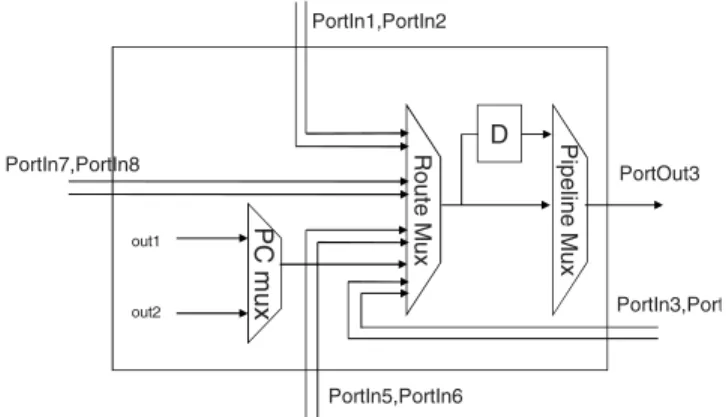
by two bidirectional arcs. This structure is detailed in Fig. 1(b). Each PE contains a processing core (PC) in the center which performs the computations, and the Port Route Boxes (PRB) at the sides which are used for signal routing. Obviously, a PE can simultaneously perform computation and several signal routings. Decoupling computation from communication has also been presented in [3] and [4]. A port is composed of two signals, an input signal (PortIn) and an output signal (PortOut). The PC has access to all input signals, the operands are selected from these input port signals by using internal multiplexors. The PC has two outputs which are distributed to all PRBs as shown in Fig. 1(b). Internal structure of a PRB is shown in Fig. 2. The selection inputs of the multiplexors in the PRB are programmed during configuration and they are fixed during program execution. The PortIn and PortOut signals are 17 bits wide, one bit is used for execution control, and the remaining 16 bits are used for data. BilRC is different
Rout e M u x P ipel ine M u x D PortIn1,PortIn2 PortIn7,PortIn8 PortIn5,PortIn6 PortOut3 PC m u x out1 out2 PortIn3,PortIn4
Figure 2. Port Routing Box (PRB) Architecture
from the architecture presented in [3] in that, BilRC does not employ a data-flow type computation model. In BilRC, execution flow is controlled by using a single control bit. In [4] on the other hand, the execution is controlled by using 5 control bits, the condition to trigger execution is programmed by using 4-input Look-Up-Tables. Another novel feature in BilRC is that, the PC has two outputs. The second output is used for various purposes such as carry output for addition, MSB output of multiplication, loop exit output for loop instructions, index of maximum calculation etc. By using the second output, arbitrary length arithmetic can be implemented.
The PC has a 1024-entry bit wide RAM, entry 16-bit wide register file (RF), a number of special purpose regis-ters, 4 data operand multiplexors, a 64-bit wide configuration register (CR) and the Execution Unit (EU). The function that the EU will perform, the operands and the port indexes of the Execute Enable signal are selected from the corresponding bit positions in the CR. The operands to the EU can either be immediate operands, i.e., constants, which are read from the RF or variables which are received from the input ports. III. A LANGUAGE FORRECONFIGURABLECOMPUTING
The architecture of the BilRC is suitable for direct map-ping of control data flow graphs (CDFG). In a CDFG every node represents a computation, and connections represent the operands. An example CDFG is shown in Fig. 3(a). In this CDFG, the node marked as ADD performs an addition operation on its two operands Op1 Data and Op2 Data when its third operand Op3 EE is activated. Here, Op1 and Op2 are data operands and Op3 is a control operand. It will be assumed a signal, x is composed of a data signal x Data and the execute enable signal x EE. Below is the LRC line for the CFDG in Fig. 3(a).
[Res, 0] = ADD(Op1, Op2) < −[Op3] (1) In LRC, the outputs are represented between the brackets on the left of the “=” sign. A node can have two outputs, for
ADD
Res_Data
Op1_Data Op2_Data Op3_EE
Res_EE (a) CDFG clock Op3_EE Op1_ODATA Op2_DATA 26 11 99 01 Res_EE Res_DATA 37 100 (b) Timing Figure 3. CDFG and Timing Diagram
this example only the first output Res is utilized. A “0” in place of an output means that it is unused, hence the second output is unused. The output Res is a 17-bit signal which is composed of 16-bit data Res Data and 1-bit EE signal, Res EE. The name of the function is provided after the equal sign. The operands of the function is given between the parentheses. The control signal which triggers the execution is provided between the brackets on the right of “< −” characters. Fig. 3(b) shows the timing diagram for the LRC example in (1). As can be seen from the timing diagram the instruction is executed when its EE input is active. The execution of an instruction takes one clock cycle, therefore Res EE signal is active one clock cycle after Op3 EE.
A typical FOR loop in LRC is given as follows: [i, i Exit] =F OR SMALLER(Start, End,
Incr) < −[LoopStart, N ext] (2) When the LoopStart signal in (2) is active, the output, i Data is assigned to the value in Start. When the signal Next is active the output is incremented by the value in Incr. When i Data reaches or exceeds the value in End, i Exit EE output is activated, which indicates that the loop is finished. The parameters, Start, End and Incr can be variables or constants. When a parameter is variable, the CDFG node receives the parameter from another node. If it is a constant the parameter is kept inside the node. In the example below all operands of the FOR SMALLER are constants.
[i, i Exit] =F OR SMALLER(1, 5, 1) < −[LoopStart, k] [k, 0] = ADD(i, i) < −[i]
[m, 0] = MUL SHIF T (i, 3, 0) < −[i]
(3) It is apparent from the LRC code that, ADD and MUL SHIFT instructions are independent, i.e., there is no data or control dependency. Hence, these two instructions execute concurrently.
LRC has support for a novel initialization mechanism which is very useful for recursive computations.
1 :[i, i Exit] = SF OR SMALLER(0, 256, 1, 0) < −[LoopStart]
2 :[A, 0] = MEM(0, i, data.txt, AddrW, DataW ) < −[] 3 :[min(32767), 0] = MIN(min, 0, A, 0)
< −[A, LoopStart]
(4)
LRC Compiler BilRC Simulator Netlist LRC Source Code Matlab or C Code High Level Simulation Verification Place & Route
Figure 4. Simulation Environment
The LRC code in (4) finds the minimum value of an array. The first instruction is SFOR SMALLER, self triggering for-loop, is similar to FOR SMALLER. However, it does not have the Next input, instead it has a 4th constant operand
which determines the number of clock cycles between loop iterations. The 2nd instruction is used for reading data from
the memory. The memory is initialized with the array in the file data.txt. The 3rdinstruction, MIN finds the minimum of
its first and third operands (second and fourth operands are used for index of minimum calculation which is not utilized in this example). The execute enable input of the MIN instruction is A EE. The second control signal between the brackets right of “< −” characters is used as initialization enable. When this signal is active, the Data part of the first output is initialized. For this example, min is initialized to the value 32767 which is in parentheses after the output signal min.
Conditional executions are inevitable in almost all kinds of algorithms. LRC has novel conditional execution control instructions. Below is a conditional assignment statement in C language:
if(A > B){result = C; }else{result = D; } (5) and its corresponding LRC code is given as:
[c result, result] = BIGGER(A, B, C, D) < −[Opr] (6) The instruction, BIGGER, executes only if its execute en-able input, Opr EE, is active. The second output result is assigned to operand C, if A is bigger than B, otherwise it is assigned to D. The first output, c result is activated only if the condition is satisfied, i.e. if A is bigger than B.
IV. TOOLS ANDSIMULATIONENVIRONMENT Fig. 4 illustrates the simulation environment. The three key components are, LRC compiler, BilRC simulator and the place & route tool. The LRC compiler takes the code written in LRC and generates a pipelined netlist. Every instruction in LRC corresponds a node in CDFG which is assigned to a PC in the BilRC and every connection between two nodes is
a net. LRC compiler maps constant operands to the register file inside the processing core. Variables are mapped to the input ports.
The BilRC simulator is implemented using SystemC. It has two main modules: the processing core (PC) and the delay element. The pipelined netlist which is produced by LRC compiler is used as the input to the BilRC simulator. The PCs are interconnected according to the nets. If a net has delay elements, then these delay elements are inserted between the PCs. The results of the simulation can be observed in three different ways: from SystemC console window, Value Change Dump (VCD) file and BilRC log files.
BilRC Place & Route tool maps the nodes of CDFG into the two dimensional architecture, and finds a path for every net. Since the interconnection architecture of BilRC is similar to that of FPGAs, similar techniques can be used for placement and routing. It must be noted that the interconnection network of BilRC is pipelined. This is the basic difference between FPGA and BilRC interconnection networks. BilRC place and route tool places the delay elements during the placement phase. The placement algo-rithm uses the simulated annealing technique. Each PE is considered as a node in the two dimensional graph. Total number of delay elements that can be mapped to a node is 4Np. For every output of a PC, a pipelined network is
formed. While placing the delay elements, contiguous delay elements are not assigned to the same node. A counter is assigned for every node which counts the number of delay elements assigned to the node. The counter values are used as a cost in the algorithm. Therefore, delay elements are forced to spread around the nodes. The routing algorithm is similar to the one presented in [5].
V. RESULTS
The performance and the resource utilization of the ap-plications mapped to the BilRC is shown in Table I. In the 3rd and 4th columns the required number of PCs and
delay elements are given respectively. The column for Np,
refers to the number of ports required for a congestion free routing of the applications on the architecture. The maximum value of Np is 4 which is only required for
the rather big LDPC decoder. The FIR, multichannel (and multirate) FIR filters have a regular computation structure. Therefore, peak and average Instruction Per Cycle (IPC) are very close to each other. In BilRC an 8×8 2D-IDCT is computed in 9 clock cycles, whereas in [6] 37 clock cycles and in [7], 54 cycles are required. This high throughput is obtained by pipelining the horizontal and vertical IDCT computations. The average IPC obtained for 2D-IDCT is 128, whereas in [8] the maximum IPC obtained is 42. The FFT is the radix-2, 1024 point FFT algorithm. By using a 2-ported memory (one for reading and one for writing), the minimum number of cycles required for the algorithm is
Table I
PERFORMANCES OFAPPLICATIONS
Application Explanation # of PCs # Delay El. Np Throughput Peak IPC Av. IPC
16 Tap FIR Frame Length=1024 33 15 1 1 sample/clock cycle 32 31.4
16 Tap Multi-Channel FIR 2 Ch., Frame Length=1024 35 31 1 1 sample/clock cycle 33 31.9
2D-IDCT 8× 8 151 91 3 1 2D-IDCT Frame / 9 clocks 142 128.3
FFT 1024 Point 33 15 2 1 Block/10359 clocks 20 17.8
Viterbi Decoder Frame Length=100 32 8 2 1 frame/809 clocks 14 3.8
UMTS Turbo Decoder Info Len=100 Rate=1/2 120 89 3 10 iterations/8590 clocks 48 29.5 CCSDC Turbo Decoder Info Len=1784 Rate=1/3 270 95 3 10 iterations/143311 clocks 111 65.4 Wimax LDPC Decoder Code Length=576 Rate=1/2 699 340 4 20 iterations/7126 clocks 252 182.2
10240. The FFT mapped on BilRC consumes 10369 cycles for one frame, only a few cycles are lost for pipelining. To our knowledge, all parts of LDPC decoding algorithm is mapped to a CGRA for the first time in this work. In [9], only the variable node processing is mapped to the CGRA (XPP-ALU arrays) with several algorithmic modi-fications. The check node processing is performed in VLIW processors. In [9], the throughput of decoding is increased by concurrently decoding more than one frame at the cost of increased latency. The maximum throughput obtained in [9] is 31.4 Mbps with a very large latency. Scaling to the same clock frequency of 400 MHz in [9], BilRC achieves almost the same throughput of 30.9 Mbps. If further throughput is required, two frames can be decoded concurrently. The Viterbi, UMTS Turbo and CCSDS Turbo decoders have a similar computation structure. These algorithms are used to decode convolutionally encoded bit streams. The complexity of the algorithms are proportional to the number of states in the convolutional coding. The Viterbi decoder has 4, UMTS has 8 and the CCSDS has 16 states. In [10], application specific processors are proposed for turbo decoders, only turbo decoders having upto 8 states are supported. In BilRC, as long as there are sufficient number of PCs, there is no limit on the number of states that can be supported. In [10], a throughput of 7.4 Mbps is obtained with an ASIP running at 335 MHz at 6 iterations. Scaling to the same frequency, the UMTS and CCSDS decoders on BilRC achieves a throughput of 6.5 Mbps and 6.95 Mbps. If further throughput is required, two sub-decoders can be employed to execute concurrently.
VI. CONCLUSION
In this paper, we have proposed a new CGRA having a very flexible interconnect network and flexible instruction set to support spatial computing. In order to program the proposed CGRA, a language, LRC is presented. LRC ef-ficiently models the CDFGs. The flexibility of BilRC and efficiency of the computation model allowed us to map several challenging algorithms onto the architecture. Com-pared to existing CGRAs, BilRC is more flexible and has a larger IPC. Compared to ASIP or ASIC implementations,
BilRC achieves almost the same performance in terms of the number of clock cycles.
REFERENCES
[1] R. Hartenstein, “A decade of reconfigurable computing: A visionary perspective,” in Proc. DATE, 2001.
[2] K. Compton and S. Hauck, “Reconfigurable computing: A survey of systems and software,” ACM Computing Surveys, vol. 34, no. 2, pp. 171–210, 2002.
[3] R. Hartenstein, M. Herz, , T. Hoffmann, and U. Nageldinger, “KressArray Xplorer: a new CAD environment to optimize reconfigurable datapath array architectures,” in Proc.
ASP-Design Automation Conference, Jan. 2000, pp. 163–168.
[4] (2010, January) Mathstar Inc., Field Programmable Object Array Architecture Guide. [Online]. Available: http://www.mathstar.com/ Documentation/ TechnicalDocs/ ArchitectureGuide ARRIX REL V1.02.pdf/
[5] L. E. McMurchie and C. Ebeling, “Pathfinder: A negotiation-based path-driven router for FPGAs,” in Proc. ACM/IEEE Int.
Symp. Field Programmable Gate Arrays, 1995.
[6] H. Singh, M.-H. Lee, G. Lu, F. Kurdahi, N. Bagherzadeh, and E. C. Filho, “MorphoSys: An integrated reconfigurable system for data-parallel and computation-intensive applica-tions,” IEEE Trans. Computers, vol. 49, no. 5, pp. 465–481, May 2000.
[7] T. Miyamori and K.Olukotun, “REMARC: Reconfigurable Multimedia Array Coprocessor,” in ACM/SIGDA FPGA, Feb. 1998.
[8] B. Mei, S. Vernalde, D. Verkest, H. D. Man, and R. Lauw-ereins, “ADRES: An architecture with tightly coupled VLIW processor and coarse-grained reconfigurable matrix,” in
Field-Programmable Logic and Applications, 2003.
[9] (2010, January) IEEE Std 802.16e LDPC Decoder on XPP-III. [Online]. Available: http://www.pactxpp.com/ main/ download/ XPP-III LDPC decoding WP.pdf/
[10] O. Muller, A. Baghdadi, and M. Jezequel, “ASIP-Based Multiprocessor SoC Design for Simple and Double Binary Turbo Decoding,” in Design, Automation and Test in Europe
(DATE 06), Mar. 2006.