Concentric Ring Structures as Efficient
SERS Substrates
Neval A. Cinel, Semih C
¸ akmakyapan, G¨ulay Ertas¸, and Ekmel ¨
Ozbay
(Invited Paper)
Abstract—Plasmonic nanopatterned structures that can work as
highly efficient surface-enhanced Raman scattering (SERS) sub-strates are presented in this study. A “coupled” concentric ring structure has been designed, fabricated, tuned, and compared to an “etched” concentric ring structure and plain gold film via SERS experiments. The proposed design gives Raman signal intensity 630 times larger than plain gold film and 8 times larger than an “etched” concentric ring structure. The surface plasmons were imaged with the fluorescence imaging technique and supporting numerical simulations were done.
Index Terms—Concentric ring, fluorescence imaging,
surface-enhanced Raman spectroscopy (SERS), surface plasmon (SP).
I. INTRODUCTION
S
URFACE-enhanced Raman spectroscopy (SERS) is a type of vibrational spectroscopy used for the fingerprinting and quantitation of molecular species. It overcomes the inefficiency of Raman spectroscopy and provides highly resolved vibrational information of the Raman-active molecules adsorbed on rough-ened metallic surfaces. Among its two primary enhancement mechanisms, electromagnetic enhancement, which states that the SER signal is enhanced proportionally to the fourth power of the local electric field intensity [1], [2] is commonly believed to be more influential than the chemical enhancement, although the subject is still under debate [3]–[6].The nanoscale surface roughnesses serve for the electromag-netic enhancement mechanism via the propagating and/or local-ized surface plasmons (SPs) that they support. Classical meth-ods such as oxidation–reduction cycling, use of metal colloids, metal island, or cold deposited films result in a heterogeneous
Manuscript received August 5, 2012; revised December 17, 2012; accepted December 17, 2012. Date of publication December 20, 2012; date of current version April 25, 2013. This work was supported by Projects DPT-HAMIT, ESF-EPIGRAT, and NATO-SET-181, and by the Scientific and Technological Research Council of Turkey under Projects 107A004, 109A015, and 109E301. The work of E. ¨Ozbay was supported by the Turkish Academy of Sciences.
N. A. Cinel and S. C¸ akmakyapan are with the Nanotechnology Re-search Center and the Department of Electrical and Electronics Engineering, Bilkent University, Ankara 06800, Turkey (e-mail: [email protected]; [email protected]).
G. Ertas¸ was with the Department of Chemistry, Bilkent University, Ankara 06800, Turkey. She is now with the Department of Chemistry, Middle East Technical University, Ankara 06800, Turkey (e-mail: [email protected]).
E. ¨Ozbay is with the Nanotechnology Research Center, Department of Elec-trical and Electronics Engineering, and the Department of Physics, Bilkent University, Ankara 06800, Turkey (e-mail: [email protected]).
Color versions of one or more of the figures in this paper are available online at http://ieeexplore.ieee.org.
Digital Object Identifier 10.1109/JSTQE.2012.2235824
distribution of nanoparticles with various sizes, shapes, and ar-rangements. However, nano roughnesses specifically designed by lithographic methods can overcome the unpredictable and irreproducible nature of SERS while increasing the Raman sig-nal intensity [7]. Moreover, this type of controlled fabrication enables the tuning of the plasmon resonances to the desired excitation wavelength [8].
Among other lithographic methods, electron-beam lithogra-phy (EBL) offers a highly controllable means to fabricate nanos-tructured arrays with minimum disparity in the shape and size of the nanoparticles. It also enables different dimension arrays to be fabricated on the same substrate at once which further facilitates the parameter optimization process and reduces the fabrication time. There are numerous reports employing EBL for SERS-active substrate designs with different nanoparticle geometries, particle shapes, sizes, and spatial arrangements yielding high SERS enhancements [7], [9]–[11].
In this study, SERS active substrates are fabricated with EBL to assemble reproducible arrays that can tailor the SERS effi-ciency and enable parameter optimization. Two different designs are prepared for comparison. The first set constitutes circular concentric rings etched from a planar gold film. In the second set, the etched portions are filled with a dielectric spacer and a second layer of golden rings are deposited only at the top of the dielectric spacer forming a coupled ring structure. The perfor-mance of “coupled ring” samples are compared to those with “etched ring” samples and “plain gold” film via SERS experi-ments and simulations. It is also shown that the design can be tuned physically for better SERS performance.
Similar designs such as concentric arcs [12] and concentric rings [13] are also available in the literature. These designs mainly depend on focusing the propagating SPs at the center of the rings. However, our motivation in this study is to show that the proposed dual layer concentric ring structure can provide increased electric field intensity due to the coupling of plasmons localized between the rings and the center disk and, therefore, be used as an efficient SERS substrate.
II. MATERIALS ANDMETHODS
A. Fabrication
The fabrication of the concentric ring samples start with the spin coating of the sapphire substrate with Poly(methylmethacrylate) (PMMA 950 A-2) resist at 2500 r/min for 40 s. It is baked for 90 s at 180 ◦C and the hydrogen silsesquioxane (HSQ), negative tone electron-beam 1077-260X/$31.00 © 2012 IEEE
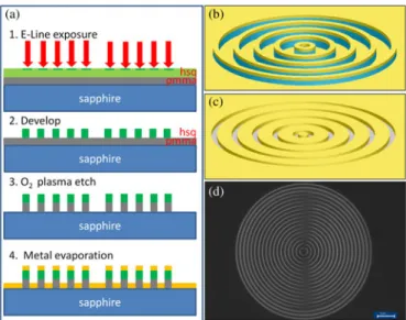
Fig. 1. (a) Illustration of fabrication steps for a five-ring “coupled” structure (b) conceptual image of “coupled” concentric rings (c) conceptual image of “etched” concentric rings (d) SEM image of the coupled structure. Inner ring diameter 965 nm, period 500 nm. The scale bar corresponds to 2 μm.
resist, is spin coated at 2000 r/min for 40 s. The substrate is then baked again for 90 s at 150◦C and aqua-save (polymer) coating is done to reduce the charging effects during e-beam exposure. Af-ter lithography is performed with the “RAITH E-Line” system, the substrate is developed in tetramethyl ammonium hydroxide (TMAH) for 75 s. A TMAH developer removes the unexposed parts of HSQ resist, leaving behind the ring patterns residing on the preserved PMMA resist layer. To remove the PMMA under the HSQ mask, O2 plasma etch is done by the “Sentech SI 500
ICP-RIE Dry Etching System” at a 50 W RF and 100 W ICP power for a duration of 30 s. Finally, 5-nm Ti adhesion layer and 40 nm Au is evaporated on the patterned sample by “Ley-bold Univex 350 Coating System.” This ends the fabrication of the “coupled ring” structure as shown in Fig. 1(b). For the “etched ring” sample shown in Fig. 1(c), a final lift off step in acetone is necessary to resolve the remaining PMMA under the upper rings. The fabrication steps are visualized in Fig. 1(a) for a 5-ring “coupled” structure. The SEM image of the resultant structure is shown in Fig. 1(d).
Physically different structures that have varying dimensions are fabricated to optimize the SERS signal intensity. The num-ber of rings for different samples are chosen as 18 considering that the increased number of rings is expected to increase the resultant E-field intensity [14]. The inner disk diameter changes from 0.965 to 1.750 um. The period of slits vary between 500 and 860 nm.
B. Imaging of SPs
There are several methods to visualize the plasmon fields accompanied by nanostructures. The most convenient method for SP imaging is to use near-field optical microscopy [15]. A more practical way is to distribute fluorescent molecules ho-mogeneously close to the metal surface and use optical mi-croscopy [16]. The fluorescent molecules should be positioned
Fig. 2. Optical microscope image (a) under white light illumination (b) imag-ing of surface under LED excitation. The scale bar corresponds to 2 μm for both figures.
at a distance from the metallic surface preferably by a few nanometers thick dielectric layer since fluorescence can quench in direct contact with the metal.
In the experimental setup, a high flux red LED is used for excitation purposes. A Leica optical microscope and its inte-grated charge-coupled devices are used to observe and image the surface. The 100× objective with numerical aperture 0.9 is used. The thin dielectric spacer is maintained by the ben-zenethiol monolayer coated for SERS measurements. No other means of dielectric deposition was necessary and no fluores-cence quenching effect was observed. A monolayer of Rho-damine 6G molecules were deposited on the spacer layer by incubating the samples for 1 h and postcleaning several times with deionized water (DI) to remove any residue after incuba-tion. Momentum matching between light and SPs is maintained by the corrugations on the gold surface. The images obtained in this way represent the SPs qualitatively rather than in a quanti-tative way [16]. The data presented in Fig. 2 are in accordance with the near-field energy density distribution measurements done with near-field scanning optical microscopy for a plas-monic lens structure made of multiple concentric metallic rings similar to our proposed design [15].
C. Simulations
A commercial software package called “Lumerical” relying on finite-difference time-domain technique is used in the simu-lations. All the physical boundary conditions are chosen as per-fectly matched layer to avoid undesired reflections from bound-aries. A maximum mesh size of 5 nm is used in the simulations to save computation time while preserving accuracy. Two-ring counterparts of the proposed structures are used for comparison to save computational sources. The physical dimensions of the disk and the rings are the same as the fabricated structures except the number of rings. The 5-nm Ti adhesion layer is excluded and a 45-nm gold layer is assumed in the simulations considering the maximum mesh size would not resolve the Ti layer. The material data for sapphire and gold are taken from the works of Palik [17] and Johnson and Christy [18], respectively. The structures are illuminated with a single wavelength plane wave source at 632.8 nm that matches the laser excitation wavelength. Two-dimensional cross-sectional monitors are used to visualize
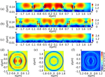
Fig. 3. Cross-sectional E -field distributions (|E|2) of the coupled resonant (a, d), coupled nonresonant (b), (e) and etched ring (c), (f) structures, respec-tively. The same color scale is used for (d), (e) and (f).
the E-field distributions. Different sized coupled structures that provide the best and worst signal intensity (corresponding to the resonant and nonresonant conditions) and etched ring structures are compared.
In accordance with the SERS experiments, the coupled struc-tures end up with a higher E-field intensity distribution and hence higher SER intensity as can be seen in Fig. 3. In the resonant-coupled structure, the upper rings are coupled to the bottom rings which results in the increase of “hot spots” respon-sible for the enhancement. This is degraded for the nonresonant structure and minimized for the etched-ring structure.
The experimentally obtained enhancement obtained from the coupled structures with respect to the etched structures is also validated by simulations. The SERS intensity is considered to be proportional to|E|4 at the laser excitation frequency for this
calculation. The E-field distributions obtained through simu-lations are integrated over the gold surfaces for both designs using 4 μm spot size. The resultant ratio gives total|E|4
coupled/
total|E|4etched∼12 which is close to the experimentally derived 8 times larger signal intensity.
III. SERS EXPERIMENTS ANDRESULTS
The SERS data are collected under excitation with an He– Ne laser at 632.8 nm with the Horiba LABRAM system. The 100× objective with a 0.9 numerical aperture is used throughout the measurements. A slit size of 200 μm and a hole size of 1100 μm ended up with the best resolution. The samples to be measured are incubated in 100 mM benzenethiol in an ethanol solution for 2 h and then thoroughly rinsed with ethanol to ensure a self-assembled monolayer formation on the surface and to remove residues. The measurements are taken right after the coating. The missing S–H bonds (at 2550–2600 cm−1, not shown in the graphs) in the SER spectrum verify that Au–S bonds are formed and indicates the formation of a monolayer [19]. Benzenethiol was purchased from Sigma-Aldrich and used as is in the Raman experiments. It has a known packing density
Fig. 4. SER spectra of Benzenethiol from the “coupled ring” structures and “plain gold” film. No background correction is done. Spectra are shifted for a better view. A horizontal axis break is applied to save space. In the legend, the letter “P ” denotes period and the letter “D” denotes diameter.
and it is a widely used molecule in SERS studies, which makes it an ideal candidate for enhancement factor (EF) calculation and comparison with previous reports in the literature.
The same integration and exposure times are used for all the samples except for the “plain gold” sample. Although four times larger integration time is used for the “plain gold” sam-ple, no distinguishable signal is observed. Considering the max-imum intensity obtained from “coupled ring” structures and the minimum detectable intensity throughout the experiment, it is derived that patterned structures have 630 times larger SER in-tensity when compared with “plain gold” film. The data are presented in stack form in Fig. 4 for easy visual comparison.
For all the fabricated samples, the number of rings is the same and the slit widths are at close proximity. Therefore, the change in signal intensity may be due to the inner ring diameter and the period. The acquired SER signal from different samples shown in Fig. 4 indicates that the sample with the smallest inner ring diameter has the largest signal intensity. One reason for this situation may be the increase in the number of rings (and, therefore, the number of hot-spots) that is included within the laser spot area, as the inner radius decreases. The increased E-field intensity is considered to be mainly due to the interaction (coupling) of the upper rings residing on dielectric and lower rings residing on sapphire. This coupling can also be visualized from the simulation results presented in Fig. 3. The period does not seem to have a major impact on the resultant signal for this design.
The effect of coupling between the upper and lower rings is also studied by comparing the “coupled” and “etched” ring structures. The coupled structures shown in Fig. 1(b) have upper and lower rings separated by a dielectric spacer layer, whereas the etched ring structures only have the lower rings as shown in Fig. 1(c). The “etched ring” structures are similar to the plasmonic lens designs that exist in the literature [14]. In a plas-monic lens structure, the period has to be chosen so as to match the SP wavelength to maximize the focusing and, therefore, the
E-field intensity that dominates the resultant SERS signal
in-tensity [20], [21]. Accordingly, the period of the “etched ring” structure is chosen to match the SP wavelength (calculated as 605 nm corresponding to the incident wavelength of 632.8 nm) in order to maximize the focusing. The SERS experiments show
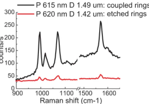
Fig. 5. SER spectrum of Benzenethiol from the “coupled” rings and the “etched” rings. No background correction is done. A horizontal axis break is applied to save space. In the legend, the letter “P ” denotes period and the letter “D” denotes diameter.
that the “coupled ring” structure that has similar physical dimen-sions with the “etched ring” structure gives eight times better signal intensity than such an optimally designed plasmonic lens structure, as depicted in Fig. 5.
An objective measure to compare the performance of dif-ferent designs existing in the literature is the EF calcu-lation. The most commonly used EF definition is EF =
(ISER S/Nsurf)/(IR S/Nvol) [22]–[24]. Here, Nsurfand Nvolare
the number of molecules probed for SERS and the Raman ex-periments; ISER S and IR S are the SERS and Raman signal
intensities, respectively. The intensity of the strongest band in the spectra at 1075 cm−1is employed for the EF calculation.
In the Raman experiment, a thin glass container with neat Benzenethiol is used where the detection volume is approxi-mated as a cylinder of height that equals the thickness of neat benzenethiol following the same steps and reasoning as in [25] and [26]. Nvolis determined from Nvol = N AρhA/M where
NA is Avogadro’s number, ρ is volume density (1.073 g/cm3),
and M is molar mass (110.18 g/mol) of benzenethiol molecules,
h is the thickness of the neat Benzenethiol, and A is the spot
area. Nsurf is defined as Nsurf − ρsA, where ρs is the surface packing density (6.8× 10¹⁴ 1/cm2) and A is the total exposed
gold area [26]. The exposed gold surface area of the structures is calculated by taking into account the lateral and top surfaces of the rings and the disk. A perfectly ordered self-assembled mono-layer is assumed on the exposed surfaces to calculate the maxi-mum possible Nsurf [23], [27], [28]. Under this assumption, the
calculated EF is an underestimate rather than an overestimate of the enhancement.
The EF calculated as described earlier is 1.67 × 10⁷ for
the coupled-concentric ring structures. On the other hand, the conventional SERS EF is on the order of 106 [29]. Therefore,
we can conclude that the coupled-concentric ring structure can be used for increasing efficiency in SERS experiments.
IV. CONCLUSION
We present here our preliminary results in designing plas-monic nanopatterned structures that can work as highly efficient SERS substrates. We relate the obtained results with theory and support with simulations. The proposed design gives 630 times larger signal intensity than “plain gold” film and 8 times larger
than an optimally designed “etched-ring” plasmonic lens struc-ture. There is still room for improvement through tuning the physical dimensions of the structures.
Future study includes the investigation of the optical re-sponses through reflection-transmission measurements and tun-ing the resonance of the structures for a better match with the laser excitation frequency to obtain a better SER signal. Under such resonant excitation, the enhancements obtained thus far are expected to increase significantly [30]. The relationship be-tween the signal intensity and the physical sizes and parameters such as slit width, number of rings, thickness, and material of the separation layer and period should also be further studied.
REFERENCES
[1] S. A. Maier, Plasmonics: Fundamentals and Applications. New York: Springer, 2006.
[2] K. Kneipp, M. Moskovits, and H. Kneipp, Surface-Enhanced Raman
Scat-tering: Physics and Applications. New York: Springer-Verlag, 2006. [3] A. Campion and P. Kambhampati, “Surface-enhanced Raman scattering,”
Chem. Soc. Rev., vol. 27, pp. 241–250, Jul. 1998.
[4] C. L. Haynes, A. D. McFarland, and R. P. Van Duyne, “Surface-enhanced Raman spectroscopy,” Anal. Chem., vol. 77, pp. 338a–346a, Sep. 2005. [5] P. L. Stiles, J. A. Dieringer, N. C. Shah, and R. R. Van Duyne,
“Surface-enhanced Raman spectroscopy,” Annu. Rev. Anal. Chem., vol. 1, pp. 601– 626, Jul. 2008.
[6] M. Moskovits, “Surface-enhanced spectroscopy,” Rev. Mod. Phys., vol. 57, pp. 783–826, 1985.
[7] M. Kahl, E. Voges, S. Kostrewa, C. Viets, and W. Hill, “Periodically structured metallic substrates for SERS,” Sensor. Actuat. B-Chem., vol. 51, pp. 285–291, Aug. 1998.
[8] N. A. Cinel, S. Butun, and E. Ozbay, “Electron beam lithography designed silver nano-disks used as label free nano-biosensors based on localized surface plasmon resonance,” Opt. Exp., vol. 20, pp. 2587–2597, Jan. 2012. [9] J. Beermann, S. M. Novikov, K. Leosson, and S. I. Bozhevolnyi, “Surface enhanced Raman imaging: Periodic arrays and individual metal nanopar-ticles,” Opt. Exp., vol. 17, pp. 12698–12705, Jul. 2009.
[10] N. Guillot, H. Shen, B. Fremaux, O. Peron, E. Rinnert, T. Toury, and M. Lamy de la Chapelle, “Surface enhanced Raman scattering optimiza-tion of gold nanocylinder arrays: Influence of the localized surface plas-mon resonance and excitation wavelength,” Appl. Phys. Lett., vol. 97, pp. 023113-1–023113-3, Jul. 2010.
[11] J. M. Oran, R. J. Hinde, N. Abu Hatab, S. T. Retterer, and M. J. Sepaniak, “Nanofabricated periodic arrays of silver elliptical discs as SERS sub-strates,” J. Raman Spectroscopy, vol. 39, pp. 1811–1820, Dec. 2008. [12] J. T. Bahns, A. Imre, V. K. Vlasko-Vlasov, J. Pearson, J. M. Hiller,
L. H. Chen, and U. Welp, “Enhanced Raman scattering from focused surface plasmons,” Appl. Phys. Lett., vol. 91, pp. 081104-1–081104-3, Aug. 2007.
[13] G. F. S. Andrade, Q. Min, R. Gordon, and A. G. Brolo, “Surface-enhanced resonance Raman scattering on gold concentric rings: Polarization depen-dence and intensity fluctuations,” J. Phys. Chem. C, vol. 116, pp. 2672– 2676, Feb. 2012.
[14] J. M. Steele, Z. W. Liu, Y. Wang, and X. Zhang, “Resonant and non-resonant generation and focusing of surface plasmons with circular grat-ings,” Opt. Exp., vol. 14, pp. 5664–5670, Jun. 2006.
[15] W. B. Chen, D. C. Abeysinghe, R. L. Nelson, and Q. W. Zhan, “Plasmonic lens made of multiple concentric metallic rings under radially polarized illumination,” Nano Lett., vol. 9, pp. 4320–4325, Dec. 2009.
[16] H. Ditlbacher, J. R. Krenn, N. Felidj, B. Lamprecht, G. Schider, M. Salerno, A. Leitner, and F. R. Aussenegg, “Fluorescence imaging of surface plasmon fields,” Appl. Phys. Lett., vol. 80, pp. 404–406, Jan. 2002. [17] E. D. Palik, “Handbook of optical-constants,” J. Opt. Soc. Amer. A, vol. 1,
pp. 1297–1297, 1984.
[18] R. W. Christy and P. B. Johnson, “Optical constants of the noble metals,”
Phys. Rev. B, vol. 6, pp. 4370–4379, 1972.
[19] S. Mahajan, M. Abdelsalam, Y. Suguwara, S. Cintra, A. Russell, J. Baumberg, and P. Bartlett, “Tuning plasmons on nano-structured sub-strates for NIR-SERS,” Phys. Chem. Chem. Phys., vol. 9, pp. 104–109, Jan. 2007.
[20] J. J. Miao, Y. S. Wang, C. F. Guo, Y. Tian, S. M. Guo, Q. Liu, and Z. Zhou, “Plasmonic lens with multiple-turn spiral nano-structures,” Plasmonics, vol. 6, pp. 235–239, Jun. 2011.
[21] H. Ditlbacher, J. R. Krenn, A. Hohenau, A. Leitner, and F. R. Aussenegg, “Efficiency of local light-plasmon coupling,” Appl. Phys. Lett., vol. 83, pp. 3665–3667, Nov. 2003.
[22] E. C. Le Ru, E. Blackie, M. Meyer, and P. G. Etchegoin, “Surface en-hanced Raman scattering enhancement factors: A comprehensive study,”
J. Phys. Chem. C, vol. 111, pp. 13794–13803, Sep. 2007.
[23] C. L. Haynes and R. P. Van Duyne, “Plasmon-sampled surface-enhanced Raman excitation spectroscopy,” J. Phys. Chem. B, vol. 107, pp. 7426– 7433, Jul. 2003.
[24] A. D. McFarland, M. A. Young, J. A. Dieringer, and R. P. Van Duyne, “Wavelength-scanned surface-enhanced Raman excitation spectroscopy,”
J. Phys. Chem. B, vol. 109, pp. 11279–11285, Jun. 2005.
[25] M. G. Banaee, P. Peng, E. D. Diebold, E. Mazur, and K. B. Crozier, “Mixed dimer double resonance substrates for surface-enhanced Raman spectroscopy,” in Proc. Conf. Lasers Electro-Opt. Quantum Electron.
Laser Sci. Conf., 2010, pp. 1–2.
[26] Y. Z. Chu, M. G. Banaee, and K. B. Crozier, “Double-resonance plasmon substrates for surface-enhanced Raman scattering with enhancement at excitation and Stokes frequencies,” Acs Nano, vol. 4, pp. 2804–2810, May 2010.
[27] L. J. Wan, M. Terashima, H. Noda, and M. Osawa, “Molecular orientation and ordered structure of benzenethiol adsorbed on gold(111),” J. Phys.
Chem. B, vol. 104, pp. 3563–3569, Apr. 2000.
[28] C. M. Whelan, M. R. Smyth, and C. J. Barnes, “HREELS, XPS, and elec-trochemical study of benzenethiol adsorption on Au(111),” Langmuir, vol. 15, pp. 116–126, Jan. 1999.
[29] L. A. Dick, A. D. McFarland, C. L. Haynes, and R. P. Van Duyne, “Metal film over nanosphere (MFON) electrodes for surface-enhanced Raman spectroscopy (SERS): Improvements in surface nanostructure stability and suppression of irreversible loss,” J. Phys. Chem. B, vol. 106, pp. 853– 860, Jan. 2002.
[30] E. C. Le Ru and P. G. Etchegoin, Principles of Surface-Enhanced Raman
Spectroscopy: and Related Plasmonic Effects. London, U.K.: Elsevier, 2009.
Neval A. Cinel received the B.Sc. and M.Sc. degrees from the Middle East
Technical University, Ankara, Turkey, in 2003 and 2006, respectively. She is currently working toward the Ph.D. degree in the Department of Electrical and Electronics Engineering, Bilkent University, Ankara.
Her research interests include biosensing, nanoplasmonics, localized surface plasmon resonance biosensors, and surface-enhanced Raman spectroscopy.
Semih C¸ akmakyapan received the B.Sc. degree from Bilkent University,
Ankara, Turkey, in 2009, where he is currently working toward the Ph.D. degree. His research interests include subwavelength plasmonic structures and the characterization, electrical, and optical properties of graphene.
G ¨ulay Ertas¸ received the B.Sc., M.Sc., and Ph.D. degrees from the Middle East
Technical University, Ankara, Turkey, in 1994, 1997, and 2003, respectively. She was an Assistant Professor Doctor in the Department of Chemistry, Bilkent University, Ankara, until February 2012. She is currently an Associate Professor Doctor in the Department of Chemistry, Middle East Technical Uni-versity. Her research interests include surface-enhanced Raman spectroscopy (SERS), magnetic microparticles, evaluation of the SERS substrate, and use of synthetic biopolymers for metal extraction.
Ekmel ¨Ozbay received the B.S. degree in electrical engineering from Middle
East Technical University, Ankara, Turkey, in 1983, and the M.S. and Ph.D. degrees in electrical engineering from Stanford University, Stanford, CA, in 1989 and 1992, respectively.
Since 1995, he has been a Full Professor in the Department of Physics and the Department of Electrical and Electronics Engineering, Bilkent Univer-sity, Ankara. His research interests include nanophotonics, nanometamaterials, nanoelectronics, nanoplasmonics, nanodevices, photonic crystals, GaN/AlGaN MOCVD growth, fabrication and characterization of GaN-based devices, and high-speed optoelectronics.
Dr. ¨Ozbay is the 1997 recipient of the Adolph Lomb Medal of the Optical Society of America and the 2005 European Union Descartes Science award.