SILICON CARBIDE HIGH VOLTAGE
DEVICES
A THESIS
SUBMITTED TO THE DEPARTMENT OF ELECTRICAL AND ELECTRONICS ENGINEERING
AND THE GRADUATE SCHOOL OF ENGINEERING AND SCIENCE OF BILKENT UNIVERSITY
IN PARTIAL FULFILLMENT OF THE REQUIREMENTS FOR THE DEGREE OF
MASTER OF SCIENCE
By
Özgür Kazar
September 2011
ii
I certify that I have read this thesis and that in my opinion it is fully adequate, in scope and in quality, as a thesis for the degree of Master of Science.
Prof. Dr. Ekmel Özbay (Supervisor)
I certify that I have read this thesis and that in my opinion it is fully adequate, in scope and in quality, as a thesis for the degree of Master of Science.
Prof. Dr. Ali Teke
I certify that I have read this thesis and that in my opinion it is fully adequate, in scope and in quality, as a thesis for the degree of Master of Science.
Assist. Prof. Dr. Ali Kemal Okyay
Approved for the Graduate School of Engineering and Science:
Prof. Dr. Levent Onural
iii
ABSTRACT
SILICON CARBIDE HIGH VOLTAGE DEVICES
Özgür Kazar
M.S. in Electrical and Electronics Engineering
Supervisor: Prof. Dr. Ekmel Özbay
September 2011
The superior properties such as wide band gap, high breakdown electric field strength, high carrier mobility, and high thermal conductivity make Silicon Carbide (SiC) preferred over Silicon (Si) and Gallium Arsenide (GaAs), in high frequency, high temperature, and high voltage applications.
SiC high voltage devices are preferred for their low reverse leakage current, low on-state voltage and resistance, high blocking voltage, and high performance at different temperatures. There are two types of the well-known SiC high voltage devices. One is Schottky diodes, which offer extremely high switching speed, but suffer from high leakage current. The other is, PiN diodes, which offer low leakage current, but show reverse recovery charge during switching and have a large junction forward voltage drop due to the wide band gap of SiC.
In this work, various SiC Schottky and PiN epilayers with different doping
concentrations between 1015 and 1016cm-3 and i-layer thicknesses between 6 and
20 µm are used. First, taking the diode radius as 1 mm, resistance and capacitance values are calculated assuming the i-layer is fully depleted. The capacitance values are much less than 100pF and the resistance values are less than 100 mΩ. The capacitance value at a reverse bias of 50 volts is calculated with another approach, which is derived from the C-V graph of the diode, assuming the diode does not have to be fully-depleted at the given bias. The resulting capacitance is 106pF. At a reverse bias lower than the breakdown voltage, the minimum capacitance value cannot be reached. Knowledge of the
iv
capacitance value in a fully depleted thickness case reveals the breakdown voltage, which was found as -3030 volts for the Poland growth SiC PiN epilayer. In the second study, the Poland growth SiC PiN epilayer with a doping concentration of 8.4*1015 cm-3 was again used. With diode diameters ranging from 0.5 mm to 3 mm and depletion thicknesses ranging from 6 µm to 100 µm, the resistance and capacitance of the diode are calculated. The minimum
resistance of 0.007Ω corresponds to the maximum capacitance of 1.05*10-10F,
whereas the minimum capacitance of 1.75*10-13 F, corresponds to the maximum
resistance of 4.4 Ω. According to the resulting data sets, the optimal diode diameter and i-layer thickness for the desired resistance and capacitance values that is needed for the switching diode design can be selected.
4H-SiC Schottky and PiN diodes with selected Ohmic, Schottky contacts and dielectric coating are fabricated. As the static characterization, we observe diodes with reverse breakdown voltages above 900 V, forward maximum current of 12.5A (current density up to 500 A/cm2), on-state diode resistance
below 10 mΩ.cm2,and a capacitance value of 50 pF at a reverse bias of 40 volts.
We also characterize the forward and reverse behaviors at different temperatures. As the dynamic characteristic, the rise-fall time is measured as 120 ns.
Keywords: Silicon Carbide, Schottky diode, PiN diode, high breakdown electric
field strength, Schottky contact, on-state voltage and resistance, capacitance, switching diode
v
ÖZET
SILICON CARBIDE YÜKSEK GERİLİM AYGITLARI
Özgür Kazar
Elektrik ve Elektronik Mühendisliği Bölümü Yüksek Lisans Tez Yöneticisi: Prof. Dr. Ekmel Özbay
Eylül 2011
Geniş bant aralığı, yüksek kırılma elektrik alan kuvveti, yüksek taşıyıcı mobilitesi ve yüksek ısıl iletkenliği gibi üstün özelliklere sahip olan Silicon Carbide (SiC) malzemesi yüksek frekans, yüksek sıcaklık ve yüksek gerilim uygulamalarında Silicon (Si) ve Gallium Arsenide (GaAs) malzemelerine tercih edilmektedir.
Düşük ters sızıntı akım, düşük ileri açılma gerilimi ve direnci, yüksek kırılma gerilimi ve farklı sıcaklıklarda yüksek performans SiC yüksek gerilim aygıtlarının tercih edilme sebeplerinin başlıcalarıdır. Anahtarlama hızı çok yüksek olmasıyla beraber PiN diyota nazaran yüksek sızıntı akıma Schottky diyotlar ve düşük sızıntı akımın yanısıra anahtarlama esnasında ters toparlanma yükü ve SiC malzemesinin geniş bant aralığı sebebiyle yüksek bileşke ileri gerilim düşmesi gösteren PiN diyotlar bilinen SiC yüksek gerilim aygıtlarının bazılarıdır.
Bu tezde katkı konsantrasyonu 1015 ile 1016 cm-3 ve intrinsic tabakası kalınlığı 6 ile 20 µm arasında değişen çeşitli SiC Schottky ve PiN epi tabakaları kullanılmıştır. İlk çalışma olarak 1mm çaplı ve intrinsic tabakası tüm yüklerden arındırılmış diyotların direnç ve kapasitans değerleri hesaplanmıştır. Kapasitans değerleri 100 pF dan, direnç değerleri ise 100 mΩ dan daha düşüktür. Ardından belirli bir ters gerilimde intrinsic tabakasının tüm yüklerden arınmış olmak
vi
zorunda olmadığı fikriyle diyotun C-V grafiği kullanılarak 50V ters gerilimde kapasitans değerleri hesaplanmıştır. Sonuç 106 pF çıkmıştır. Kırılma geriliminden daha düşük gerilimlerde en düşük kapasitans değerine ulaşılamamaktadır. Intrinsic tabakası tüm yüklerden arındırılmış diyotun kapasitans değeri bilgisi kırılma gerilimini buldurmaktadır. Bu değer Polonya büyütmesi SiC PiN epi tabakası için -3030V olarak hesaplanmıştır. İkinci
çalışmada da 8.4*1015 cm-3 katkı konsantrasyonuna sahip Polonya büyütmesi
SiC PiN epi tabakası kullanılmıştır. Diyot çapı 0.5 ile 3 mm arasında, intrinsic tabakası kalınlığı ise 6 ile 100 µm arasında alınarak direnç ve kapasitans değerleri hesaplanmıştır. En düşük direnç değeri 0.007Ω en yüksek kapasitans
değeri 1.05*10-10 F a denk gelirken, en düşük kapasitans değeri 1.75*10-13 F en
yüksek direnç değeri 4.4Ω a denk gelmektedir. Elde edilen verilere göre anahtar diyot tasarımının gerektirdiği direnç ve kapasitans değerleri için en uygun diyot çapı ve intrinsic katmanı kalınlığı seçilebilmektedir.
Seçilmiş ohmik, Schottky kontaklarla ve dielektrik kaplamayla 4H-SiC Schottky ve PiN diyotlar üretilmiştir. Statik karakterizasyon olarak diyotların
kırılma gerilimi 900V dan yüksek, ileri en yüksek akımı 12.5 A (500 A/cm2 e
kadar akım yoğunluğu), ileri konum direnci 10 mΩ.cm2 den düşük ve 40 V ters
gerilimde kapasitansı 50 pF olarak ölçülmüştür. İleri ve ters konumdaki ölçümler farklı sıcaklıklarda da gerçekleştirilmiştir. Dinamik karakterizasyon olarak yükselme ve düşme süreleri 120 nsec olarak ölçülmüştür.
Anahtar Kelimeler: Silicon Carbide, Schottky diyot, PiN diyot, yüksek kırılma
elektrik alan kuvveti, Schottky kontak, ileri açılma gerilimi ve direnci, kapasitans, anahtar diyot
vii
Acknowledgements
It is my pleasure to express my deepest gratitude to my supervisor Prof. Dr. Ekmel Özbay for his invaluable guidance, motivation, encouragement, confidence, understanding, and endless support. My graduate study under his supervision was my lifetime experience. It was an honor to work with him, and I learned a lot from his superior academic personality.
I would like to thank the members of the thesis committee, Prof. Dr. Ali Teke, Assist. Prof. Dr. Ali Kemal Okyay for their useful comments and suggestions. I would also like to thank all the former and present members of NANOTAM and Advanced Research Laboratory for their continuous support. It was a pleasure to work with these hard-working guys in the same group.
I am also grateful to my close friends for their valuable support in every step of my life.
Finally I would express my endless thank to my family; Kemal, Mualla, Barış and Neslihan for their understanding and continuous moral support. Very special thanks belong to my future wife, Merve, for her endless moral support, understanding, and love.
viii
Table of Contents
Abstract……….iii
Özet………v
Acknowledgements……….vii
Table of Contents………...viii
List of Figures………....x
List of Tables………...xii
1. Introduction and Thesis Outline………1
2. Silicon Carbide: Material and Electronic Device Design………..4
2.1. Historical Background……….4
2.2. Material Properties………..5
2.3. Electronic Properties………...6
2.4. Theory and Drift Layer Design………...7
2.5. Microwave Shunt and Series Circuit Models………14
2.6. 3kV SiC PiN Diode Design………...16
3. Fabrication Process Steps………18
3.1. Wafer Cleaving and Cleaning………....18
3.2. Photolithography and Development………..20
3.3. Ohmic and Schottky Metallization………23
3.4. Lift-off………...24
3.5. Annealing (Rapid Thermal Annealing)……….26
3.6. Dielectric Coating………..26
ix
4. Characterization………...33
4.1. SiC Schottky Diodes………..33
4.1.1. Reverse Breakdown Voltage……….33
4.1.2. Maximum Forward Current, Resistance and
On-Voltage………34
4.1.3. Switching Characteristics………..38
4.1.4. Temperature Dependent Forward Current………39
4.1.5. Temperature Dependent Leakage Current………40
4.1.6. Diode Off-Capacitance………..41
4.2 .SiC PiN Diodes………..42
4.2.1 Reverse Breakdown Voltage………42
4.2.2 Maximum Forward Current, Resistance and
On-Voltage……….42
4.2.3 Switching Characteristics……….45
4.2.4 Diode Off-Capacitance……….46
4.3 .Conclusion...47
5. Summary and Future Suggestions……….…...49
x
List of Figures
Figure 2.1 Linear Fit of 1/C
2- DC Bias……….9
Figure 2.2 Low-field electron mobility as a function of doping
concentration in 4H SiC (perpendicular to the c-axis, T = 300 K).
Full circles: experimental data from [4]; open circles: experimental
data from [13]; open squares: experimental data from [14]; open
triangles: experimental data from [1], full line: fit………...12
Figure 2.3 Resistance and Capacitance values of Poland 420/421
growth epilayer as a function of the depletion thickness and diode
area………13
Figure 2.4 Series SPST Switch………15
Figure 2.5 Shunt SPST Switch……….15
Figure 3.1 Photographs of fabricated SiC Schottky and PiN
diodes………....19
Figure 3.2 Photographs of quartz photo mask……….20
Figure 3.3 Direct and Image-reversal Photolithography…………..22
Figure 3.4 Alignment and development Microphotographs………23
Figure 3.5 Lift-off process, both for direct and image-reversal
xi
Figure 3.6 Lateral Structure of Schottky Diode………...31
Figure 3.7 Lateral Structure of PiN Diode………...32
Figure 4.1 Breakdown voltage of SiCrystal 0539-A2………..34
Figure 4.2 a) Maximum Forward Current b) Differential
On-Resistance of SiCrystal 0539-A2………..36
Figure 4.3 100mA limited Forward I-V graph of SiCrystal 0539-A2,
(a) Linear, (b) Logarithmic………...37
Figure 4.4 SiC Schottky diode Rise and Fall Time………..38
Figure 4.5 SiC Schottky Diode temperature dependent forward
characteristics………39
Figure 4.6 SiC Schottky Diode temperature dependent reverse
characteristics………40
Figure 4.7 SiC Schottky Diode total capacitance (C
T) with respect to
reverse bias voltage………...41
Figure 4.8 Breakdown voltage of PiN 545/546 Poland…………...42
Figure 4.9 a) Maximum Forward Current b) Differential
On-Resistance of PiN 545/546 Poland………43
Figure 4.10 100mA limited Forward I-V graph of PiN 545/546
Poland, (a) Linear, (b) Logarithmic………..44
Figure 4.11 SiC PiN diode Rise and Fall Time………45
Figure 4.12 SiC PiN Diode total capacitance (C
T) with respect to
reverse bias voltage………...46
xii
List of Tables
Table 2.1 Doping concentration, mobility, resistivity, diode area,
and the depletion thickness of different epilayers……….10
Table 2.2 Minimum capacitance and resistance values for different
epilayers ………...10
Table 2.3 Capacitance value at a reverse bias of 50 volts for Poland
420/421 growth epilayer………...11
Table 2.4 Capacitance value of fully depleted Poland 420/421
growth epilayer along with breakdown voltage of the epilayer……11
Table 2.5 Resistance and Capacitance of Poland 420/421 growth
epilayer, at 50 volts and 3000 volts of reverse bias such that 3000
volts of reverse bias is the breakdown voltage of the epilayer…….17
Table 2.6 Insertion loss and isolation calculation in dB units……..17
Table 3.1 Detailed fabrication recipes of SiC Schottky and PiN
diodes………28
1
Chapter 1
Introduction and Thesis Outline
Power semiconductor devices are a key component of all power electronic systems. It is estimated that at least 50 percent of the electricity used in the world is controlled by power devices. With the widespread use of electronics in the consumer, industrial, medical, and transportation sectors, power devices have a major impact on the economy because they determine the cost and efficiency of systems. After the initial replacement of vacuum tubes by solid state devices in the 1950s, semiconductor power devices based on silicon material took a dominant role [27]. Silicon has long been the dominant semiconductor of choice for high-voltage power electronics applications [20, 21]. However, with the passage of time, the demands on electronic devices are rapidly changing from low power/speed to high power/speed with their compatibility in very harsh temperature, high pressure, and corrosive environments. The physical properties of Si do not meet such demands. Wide
2
bandgap semiconductors, particularly Silicon Carbide (SiC) and Gallium Nitride (GaN), have begun to attract much attention because they are projected to have much better performance than silicon [22-26]. The advantage of wide bandgap materials is due to their outstanding material properties. Power electronics devices based on wide bandgap semiconductor materials will likely result in substantial improvements in the performance of power electronics systems in terms of higher blocking voltages, efficiency, and reliability, as well as reduced thermal requirements [29].
Silicon carbide (SiC) is a semiconductor material with suitable properties for high-power, high-frequency, and high temperature applications. Silicon carbide is a wide bandgap semiconductor material with high breakdown electric field strength, high saturated drift velocity of electrons, and a high thermal conductivity. Due to its higher thermal conductivity, silicon carbide material can operate at higher temperatures without the destruction of the device. In addition, silicon carbide is also extremely radiation hard, which means that radiation does not degrade its electronic properties [11]. In addition to these properties, a native substrate of SiC with reasonable size exists, and it can be doped with both n- and p-types. Moreover, SiC, like silicon (Si), has SiO2 as its stable native oxide.
These properties make SiC ideally suited for a number of applications such as unipolar devices: Schottky diodes, junction field effect transistors (JFETs), and metal oxide semiconductor field-effect transistors (MOSFETs) and bipolar devices: PiN diodes [28].
Silicon carbide power devices based on its 4H polytype (4H-SiC) have the potential to revolutionize the power semiconductor industry. Benefitting from an order of magnitude larger critical breakdown electric field than silicon (Si) and sufficiently high carrier mobility, 4H-SiC power devices are designed with thinner, and heavily doped drift layers enabling ultra high voltage capability with minimal conduction and switching losses [19].
Many companies have been producing SiC as a semiconductor material for more than twenty years. Recently, defect density has been reducing to a level low
3
enough to allow the fabrication of large area power devices. At the same time, the cost is dropping in order to compete with silicon power diodes [8].
In this work, we study the drift layer design of SiC high voltage devices and design a microwave 1GHz 3kV SiC PiN diode switch. We fabricate SiC Schottky and PiN diodes with various diode diameters and depletion layer thicknesses. Finally, we demonstrate our best effort.
This thesis consists of five chapters including this introduction.
In chapter 2, we give a historical background of Silicon Carbide material and study its material and electrical characteristics. Then, we move on to the theory and drift layer design of high voltage SiC devices. After that, possible microwave shunt and series circuit models are explained with isolation and insertion loss parameters. At the end of the chapter, a 3kV SiC PiN diode switch design is given.
In chapter 3, we study the detailed process steps during the fabrication of SiC Schottky and PiN high voltage devices. All of the processes were completed at the Nanotechnology Research Center within a Class-100 clean room environment. The chapter finishes with the recipes of SiC Schottky and PiN diode fabrications.
The characterization of the fabricated diodes is performed in chapter 4. Both static and dynamic characteristics of SiC Schottky and PiN diodes, as well as the measurement setups are presented. We begin with I-V characteristics; reverse breakdown voltage, forward maximum current and on-resistance, and then move on to the switching behaviors. Finally, we present the capacitance-voltage measurements, which gives an idea about the doping concentration of the drift layer (2.4), as a necessary design parameter for a practical SiC PiN diode.
The summary and conclusion of the research is given in chapter 5, which also includes critiques of our work and future plans.
4
Chapter 2
Silicon Carbide: Material and
Electronic Device Design
In this chapter, firstly, the historical background, material and electronic properties of Silicon Carbide (SiC) material are given. Then, the theory and drift layer design of high voltage SiC devices are studied. After that, microwave shunt and series circuit models along with isolation and insertion loss are presented. Finally, the chapter is finished with a practical 3kV SiC PiN diode switch design.
2.1 Historical Background
The first report on silicon carbide was published in 1824 by the Swedish chemist Jöns Jacob Berzelius, Professor in chemistry at the Karolinska Institute in Stockholm [30]. Berzelius burnt an unknown compound and observed an equal
5
number of silicon (Si) and carbon (C) atoms [10]. In 1905, Henri Moissan found out that SiC occurred in nature when he investigated a meteorite from Cañon Diablo, Arizona, USA [31]. American inventor Edward Acheson first made Silicon Carbide (SiC) in 1891 while he was trying to make a diamond [8]. He worked for the synthesis of “carborundum” to be used as an abrasive material, however the crystal quality was not sufficient for studies till 1950s [35]. In 1955, J. A. Lely developed a process for producing the pure SiC single crystals with high quality [32], and in 1959 the first SiC conference was held in Boston. In the 1960s and 1970s Silicon (Si) technology became dominant and the work on SiC was centered on basic solid-state physics and crystal growth. In the early 1980s, Tariov presented the seeded sublimation growth technique to grow SiC bulk crystals [33], and Matsunami made it possible to grow cubic single crystalline SiC on silicon substrates [34]. In the 1990s, limitations to the silicon and III-V technologies came out and the interest for SiC started to grow and has been substantial since then [35]. In recent years, the development of SiC devices has made significant progress and demonstrated advantages over Si devices in the area of high power electronics due to its superior physical and electrical properties [10]. As with all new technologies, the cost was stayed as the limiting factor on marketing the SiC based devices widespread. Cree and some other companies have been utilizing Silicon Carbide as a semiconductor material for more than 20 years in the production of blue and green LEDs. Recently, the defect density has been reduced to a level low enough to allow the fabrication of large area power devices with an acceptable yield. At the same time, material costs are dropping and a realistic competition with silicon power devices is rising [8].
2.2 Material Properties
The chemically stable form of silicon (Si) and carbon (C) is silicon carbide (SiC). SiC consists of Si and C atoms, where each Si atom shares electrons with four C atoms, that is, each atom is bonded covalently to four neighbors and vice
6
versa, in a tetrahedral arrangement. SiC occurs in many different crystal structures, called polytypes. The polytypes differ in the stacking sequence of Si-C double layers. The polytype notation is composed of a number, specifying the number of planes, where each plane is a double layer of Si and C atoms, in the stacking sequence; and a capital letter, indicating the resulting structure of the crystal. For instance, the sequence is ABC for 3C-SiC, ABAC for 4H-SiC, and ABCACB for 6H-SiC. Within 250 polytypes of silicon carbide, three types are commonly grown for use as an electronic semiconductor. These are; cubic polytype devoted as 3C- or β-SiC, hexagonal polytypes denoted as 2H-, 4H-, 6H-SiC; and rhombohedral polytypes denoted as 15R-, 21R-, 27R-SiC. The hexagonal and rhombohedral polytypes are collectively referred as α-SiC. The most common polytypes for electronic devices are 3C-, , and 6H-SiC. 4H-SiC is the preferred polytype for device processing, with higher and more isotropic carrier mobility than 6H-SiC, which is essential for achieving low on-resistance, and wider band gap than 3C- and 6H-SiC.
2.3 Electronic Properties
SiC, owing almost three times wider band gap than silicon allows high temperature operation. In wider band gap materials, higher energy is needed to excite an electron from a valence band to a conduction band and forms an electron-hole pair. Hence, SiC enters its intrinsic region at a higher temperature compared to silicon [11]. The operating temperature of SiC based devices is 4 or 5 times higher than Si counterparts. Besides for the wide band gap, SiC has a critical electric field of 2 ~ 4 MV/cm, which is almost ten times higher than silicon, under reverse bias [15]. This means an almost ten times higher breakdown voltage rating for SiC based devices compared to silicon counter parts. As a result, the drift layer of such high voltage devices can be designed 10x thinner and 100x highly doped [10, 15]. The resistance of the power diode with such a thinner and highly doped drift layer is 1000x lower (2.1, 2.2). The switching speed of SiC devices is nearly 30 times higher than Si counterparts.
7
The thermal conductivity is 4 times higher than Si, which enables un-cooled
operation. With a sufficient electron mobility of ~1000cm2/Vs [16], this value is
only 20% less than Si counterparts.
2.4 Theory and Drift Layer Design
SiC high voltage devices are preferred for their low reverse leakage current, low on-state voltage and resistance, high blocking voltage, and high performance at different temperatures. Schottky diodes, which offer extremely high switching speed, but suffer from high leakage current, and PiN diodes, which offer low leakage current, but show reverse recovery charge during switching and have a large junction forward voltage drop due to the wide band gap of SiC, are two of the well-known SiC high voltage devices [12]. In a Schottky diode, being a unipolar majority carrier device, only electrons are injected from the semiconductor into the Schottky metal layer, in turn resulting in forward current. Since no holes are injected into the semiconductor, there is no stored charge and no reverse recovery transient and, therefore, the SBD turns off very rapidly. However, PiN diodes, being a bipolar minority carrier device, have reverse recovery current [9]. They consist of heavily doped p+ and n+ end regions separated by a lightly doped region that can usually be regarded as intrinsic. It operates as a variable resistor at radio and microwave frequencies. At zero or reverse bias, the intrinsic layer represents high resistance, whereas, under forward bias, the carriers reduce the resistance of the intrinsic layer [5]. The low loss RF device, PiN diode is resistive under forward-bias, and capacitive under zero or reverse-bias. These two parameters are mainly determined by the doping concentration of the I-layer. The capacitance of the diode is closely related to the reverse blocking voltage and leakage current (2.4). As the other important parameter, the resistance of the diode is also in relation with the blocking voltage, such that these diodes have very high blocking voltages that result in
8
high on-resistance [16]. The way to reduce on-resistance is to increase the doping concentration of the intrinsic drift layer [6] (2.1, 2.2).
However, besides for other limitations, there is a significant obstacle that keeps the doping concentration at convenient values. In a typical PiN diode, both holes and electrons inject into the intrinsic drift layer in forward conduction mode. In addition, some reverse bias is needed to deplete this region of mobile charge. In a highly doped intrinsic region, it becomes harder to deplete the carriers. These mobile carriers in the depletion region result in current flow at reverse bias, which is called leakage current [2].
In the highly doped I-layer, the depleted thickness is lower, due to its relatively depleted state at a given reverse bias. With a relatively low depleted thickness, it is infeasible to obtain lower capacitance values (2.3).
In (2.3), the parameter “L” is the depleted thickness of the I-layer. Assuming the thickness of I-layer as “L”, (2.3) gives us the capacitance of the fully-depleted PiN diode layer. Therefore, it is easy to find the minimum capacitance of the I-layer. However, as mentioned hereinabove, at a given bias, it is erroneous to say that the whole I-region is depleted of mobile charges. Therefore, with (2.3), we cannot determine the depleted thickness at a given bias, and thus cannot determine the capacitance.
There is another approach for finding the capacitance of the PiN diode, which is
9
function of V (Fig. 2.1) gives us a relation between the doping concentration and capacitance [3] (2.4).
Therefore, optimal doping concentration values of I-layer are set, in order to keep the resistance and capacitance of the diode lower.
Fig. 2.1: Linear Fit of 1/C2 - DC Bias
-12 -10 -8 -6 -4 -2 0 2 4 0,00E+000 1,00E+019 2,00E+019 1/C^2 DC bias (V) B Linear Fit of B Equation y = a + b*x Adj. R-Square 0,99996
Value Standard Error B Intercept 4,76282E18 2,42292E15 B Slope -1,678E18 1,11667E15
10
Cree-‐D Cree-‐E Poland 420/421 Poland 545/546
q (As) 1,60E-‐19 1,60E-‐19 1,60E-‐19 1,60E-‐19
μ (cm2/Vs) 825 910 860 860
n (cm-‐3) 1,70E+16 3,00E+15 8,40E+15 8,40E+15
ρ (Ωcm) 4,46E-‐01 2,29E+00 8,65E-‐01 8,65E-‐01
ρ (Ωm) 0,00446 0,0229 0,00865 0,00865
Diode radius (m) 1,00E-03 1,00E-03 1,00E-03 1,00E-03
Diode Area (m2) 3,14E-‐06 3,14E-‐06 3,14E-‐06 3,14E-‐06
Depletion
thickness (m) 6,00E-‐06 1,00E-‐05 2,00E-‐05 2,00E-‐05
ε0 (F/m) 8,85E-‐12 8,85E-‐12 8,85E-‐12 8,85E-‐12
εR (SiC) 10,1 10,1 10,1 10,1
Table 2.1: Doping concentration, mobility, resistivity, diode area, and the depletion thickness of different epilayers
In Table 2.1, four different SiC PIN epilayers with different doping concentrations and I-layer thicknesses are given. The mobility (µ) is dependent on the doping concentration [7] and we determine mobility from Fig. 2.2 for each epilayer. Resistivity (ρ) is calculated for all of the epilayers (2.2). We assume all of the diodes have a radius of 1mm. As a first study, we simulate as if all the epilayers are fully depleted of charges. Following this assumption, we find the resistance and capacitance of the diodes as follows:
Cree-‐D Cree-‐E Poland 420/421
Poland 545/546
capacitance (F) 4,68E-‐11 2,80E-‐11 1,40E-‐11 1,40E-‐11
resistance (Ω) 0,00851 0,0728 0,0550 0,0550
Table 2.2: Minimum capacitance and resistance values for different epilayers Using (2.1), (2.2), and (2.3) we find the minimum capacitance and resistance values of each diode (Table 2.2). However, targeting a capacitance value at a given bias as a design constraint requires a different approach, knowing the fact that the diode does not have to be fully-depleted at the desired voltage value. In order to find the targeting capacitance at a bias voltage, we use (2.4).
11
Concerning Fig. 2.1, Vi is the intercept along the voltage axis in 1/C2-V graph.
Table 2.3 shows the capacitance value at a reverse bias of 50 volts for the Poland 420/421 epilayer.
Poland 420/421
Vi 2,836
Vbias -‐50
Capacitance @ Vbias (F) 1,06E-‐10
Table 2.3: Capacitance value at a reverse bias of 50 volts for Poland 420/421 growth epilayer
It is clear that capacitance at a reverse bias of 50 volts is larger than the capacitance at full depletion (Table 2.2, 2.3). Therefore, more reverse bias is needed to deplete all of the mobile charges in the I-layer. Again using (2.4), along with knowledge of the capacitance value of fully depleted Poland 420/421 epilayer, we find full-depletion voltage as 3030 volts (Table 2.4).
Poland 420/421
Vi 2,836
Vbias -‐3030
Capacitance @ Vbias (F) 1,40E-‐11
Table 2.4: Capacitance value of fully depleted Poland 420/421 growth epilayer along with full-depletion voltage of the epilayer
12
Figure 2.2: Low-field electron mobility as a function of doping concentration in 4H SiC (perpendicular to the c-axis, T = 300 K). Full circles: experimental data from [4]; open circles: experimental data from [13]; open squares: experimental data from [14]; open triangles: experimental data from [1], full line: fit.
In the next study, the Poland 420/421 growth SiC PiN epilayer with a doping
concentration of 8.4*1015 cm-3 is used. With diode diameters ranging from 0.5
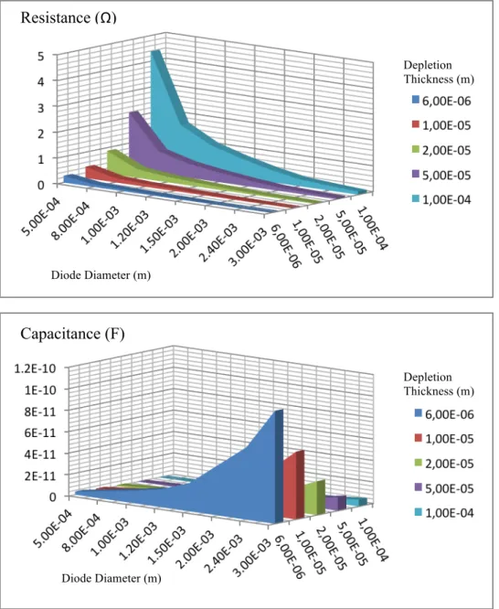
mm to 3 mm and depletion thicknesses ranging from 6 µm to 100 µm, the capacitance and resistance of the diode are calculated using (2.1), (2.2), and (2.3). Selecting the maximum diode diameter of 3mm and minimum epilayer thickness of 6µm, results in a minimum resistance of 0.007Ω and maximum
capacitance of 1.05*10-10 F. In contrast, selecting the minimum diode diameter
of 0.5 mm and maximum epilayer thickness of 100 µm, ends up with minimum
capacitance of 1.75*10-13 F and maximum resistance of 4.4 Ω (Fig. 2.3).
According to the results, we conclude that there is a trade-off between diode resistance and capacitance and, therefore, we should select the optimal diode diameter and I-layer thickness for the aimed design constraints such as the target capacitance, breakdown voltage, or resistance value.
13
Figure 2.3: Resistance and Capacitance values of Poland 420/421 growth epilayer as a function of the depletion thickness and diode diameter
Diode Diameter (m) Resistance (Ω) Capacitance (F) Diode Diameter (m) Depletion Thickness (m) Depletion Thickness (m)
14
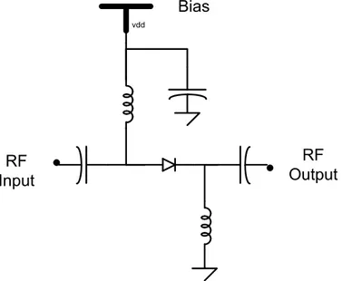
2.5 Microwave Shunt and Series Circuit Models
A typical PiN diode switch operates as a bridge between RF input and RF output in a microwave circuit. Depending on the circuitry, the switching is based on the forward and reverse characteristics of the diode [18]. An ideal switch shows zero impedance at forward bias and infinite impedance at reverse bias. We expect small impedance in the ON state and finite impedance in the OFF state, as working in the lower microwave frequency range. Two of the fundamental parameters that describe PiN diode switch performance are isolation and insertion loss. Isolation is a measure of how effectively a switch is turned OFF. We define isolation as the difference between the power at the switch output with the switch ON and the power at the switch output with the switch OFF. Insertion loss is the transmission loss during the ON state of the switch. We define insertion loss as the difference between the power at the output with no switch and the power at the output with the switch ON [2].
Single Pole Single Throw (SPST) Switches are composed of Series and Shunt Switches. In series SPST switch, insertion loss depends on the forward series resistance and isolation depends on the reverse capacitance. The related equations are given in (2.5) and (2.6).
dB (2.5) dB (2.6)
where, Ct is reverse capacitance, Rs is forward resistance, f is the frequency and
15 vdd RF Input RF Output Bias
Figure 2.4: Series SPST Switch
In the shunt SPST switch, unlike series, insertion loss is dependent on reverse capacitance and isolation depends on forward resistance. The related equations are given in (2.7) and (2.8). Fig. 2.4 shows the shunt SPST Switch RF circuit.
dB (2.7) dB (2.8) vdd RF Input RF Output Bias
16
2.6 3kV SiC PiN Diode Design
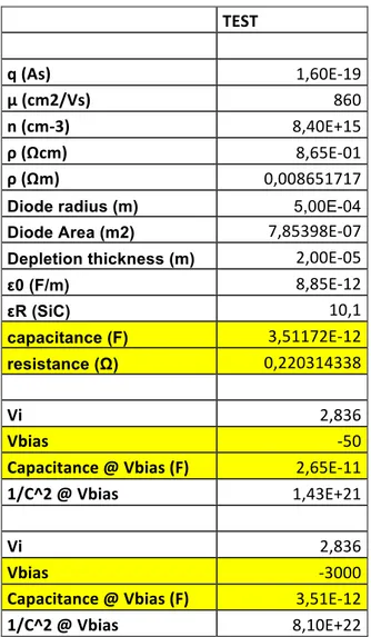
In this section, a practical SiC PiN diode design with the Poland 420/421 epilayer, which is to be used as a microwave switch at 1GHz, is presented. In the previous parts, we found the resistance, capacitance, and breakdown voltage of diodes with different diode areas defined in our photo mask and possible epilayer thicknesses. We also studied microwave series and shunt diode designs for switching RF circuit. Shunt circuit model is better for higher isolation and low insertion loss due to the non-presence of the diode on the transmission line.
The doping density of Poland 420/421 epilayer is 8.4*1015 cm-3. As design
constraints, we are asked to obtain a capacitance of 50 pF at 50 volts of reverse bias and resistance below 0.5 Ω. Moreover, insertion loss should not be higher than 2 dB and isolation should be at least 25 dB. In order to meet the criteria, we need to find the optimum diode radius (area) and minimum depletion thickness. Using equations (2.1), (2.2), (2.3), and (2.4); with a diode radius of 0.5 mm and depletion thickness of 20 µm, a capacitance of 26.5 pF at 50 volts of reverse bias and resistance of 0.22 Ω are obtained. Equating (2.3) and (2.4), the breakdown voltage of the diode is 3000 V (Table 2.6).
With forward series resistance of 0.22 Ω and reverse capacitance of 3.51 pF, insertion loss and isolation are 1.15 dB and 41.2 dB, respectively (Table 2.7). We meet the criterion of the shunt switch as well.
17 TEST q (As) 1,60E-‐19 μ (cm2/Vs) 860 n (cm-‐3) 8,40E+15 ρ (Ωcm) 8,65E-‐01 ρ (Ωm) 0,008651717
Diode radius (m) 5,00E-04
Diode Area (m2) 7,85398E-‐07
Depletion thickness (m) 2,00E-‐05
ε0 (F/m) 8,85E-‐12 εR (SiC) 10,1 capacitance (F) 3,51172E-‐12 resistance (Ω) 0,220314338 Vi 2,836 Vbias -‐50
Capacitance @ Vbias (F) 2,65E-‐11
1/C^2 @ Vbias 1,43E+21
Vi 2,836
Vbias -‐3000
Capacitance @ Vbias (F) 3,51E-‐12
1/C^2 @ Vbias 8,10E+22
Table 2.5: Resistance and Capacitance of Poland 420/421 growth epilayer, at 50 volts and 3000 volts of reverse bias such that 3000 volts of reverse bias is the
breakdown voltage of the epilayer
Forward Resistance (Rs) (Ω) Load Impedance (Zo) (Ω) Reverse capacitance (Ct) (F) RF frequency (f) (Hz) Insertion Loss (dB) Isolation (dB) 0,22 50 3,51E-‐12 1,00E+09 1,15 41,18644803
18
Chapter 3
Fabrication Process Steps
In this chapter, the details of the fabrication of SiC Schottky and PiN High Voltage High Current Diodes are explained. All the processes were completed at the Nanotechnology Research Center within a Class-100 clean room environment.
3.1 Wafer Cleaving and Cleaning
Cleaving and cleaning of wafers before fabrication is a fundamental step that is to be taken seriously. As working with expensive SiC wafers, it is a good idea to cleave 2 inch wafers into many small pieces. Working with the 9 mm x 9 mm mask size, it is ideal to use a 10 mm x 10 mm sample size. The traditional way to prepare small pieces from 2 inch wafers is to scratch the back side of the substrate of a desired length, using a diamond tipped scriber pen. SiC is a tough material and it is easy to cleave small square samples without arbitrary shapes.
19
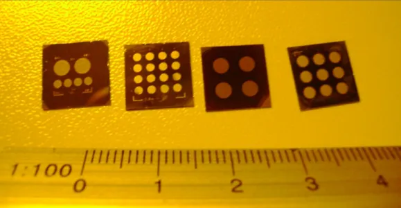
However, even a 10 mm x 10 mm sample is considerably expensive and it is not a good idea to waste one more sample for a single fabrication. In addition, the edges of the sample may be rough from using a scriber pen. It becomes harder to hold the sample during the whole fabrication steps. Therefore, a solution for cleaving is performed in our fabrication. We use Disco Automatic Dicing Saw DAD 3220 for the cleaving process of 2 inch SiC wafers. In this case, we have the opportunity of selecting the size of the samples. We obtain very sharp and accurate edges. In Figure 3.1, photographs of fabricated SiC Schottky and PiN diodes are shown.
Figure 3.1: Photographs of fabricated SiC Schottky and PiN diodes
At the very beginning and after each fabrication steps, cleaning is crucial. We perform a process called three solvent cleaning. First, the sample is dipped into boiling trichloroethane for 2 minutes. Then, the sample is kept in acetone for 5 minutes at room temperature. Finally, sample is dipped into boiling isopropanol for 2 minutes. Sequentially, oil, organic molecules or photo resist, and acetone are dissolved. After the three solvent cleaning processes, the sample is washed with deionized (DI) water and dried with a nitrogen gun. Even the very small water drop is vaporized with dehydration bake at 120°C for 2 minutes. An optical microscope is used to check the cleanliness of the sample at each step.
20
3.2 Photolithography and Development
Photolithography is the transfer of patterns from the photo mask to the sample surface. UV sensitive material, named photo resist, is coated on the surface of the sample using a Specialty Coating Systems spinner. Photolithography is performed at every fabrication step in order to define the regions to be coated or etched.
Photolithography starts with surface cleaning and resist coating. We use AZ5214E and TI35ES type photo resists. Process parameters for TI35ES are given in Table 3.1. For now, we continue with the AZ5214E type. Using the spinning parameters of 4000rpm and 40 seconds, the resulting resist thickness on the substrate is 1.4µm. The process continues with the soft-bake of the resist at 110°C for 55 seconds before exposure. The photographs of the quartz photo mask are given in Fig. 3.2.
Figure 3.2: Photographs of quartz photo mask
The photo mask is used for the selective exposure facing the substrate. We use a Karl Suss MA6 Mask Aligner for the alignment and exposure process. Both a photo mask and substrate coated with resist are loaded to the system. After proper alignment, the sample is subjected to UV exposure in “Hard” exposure
mode for 4.5 seconds with an 8mW/cm2 HG lamp. Depending on the patterns,
the photo resist under UV radiation becomes soluble in the developer. This is direct photolithography, which can be used for mesa etching. For the
image-21
reversal photolithography, after the first bake, the sample is subjected to UV exposure in “Hard” exposure mode for 1.5 seconds. After the exposure, we wait for 5 to 10 minutes following the image-reversal hard-bake at 110°C for 2 minutes. The exposed photo resist becomes inert. Then, the sample is again subjected to UV exposure in “Flood-E” exposure mode for 4.5 seconds; but this time without a photo mask. The photo resist, which was not subjected to UV radiation in the first step, becomes soluble in the developer after these steps. This lithography can be used for thick metallization lift-off. Figure 3.3 shows direct and image-reversal photolithography.
22
Photolithography
Image-Reversal Direct
Lithography Lithography
Bake Development
Development
23
The final step of photolithography is the development of the exposed samples.
We use the developer AZ400K with 1:4 (AZ400K:H2O) ratio. The optimized
developer time for the photolithography parameters given above is approx. 40 seconds. Etching away the soluble photo resist with a significant color change on the substrate can be followed by the naked eye. The substrate is dipped into DI water when one is ensured that this color change stops. Finally, the substrate is dried with a nitrogen gun. The photolithography should be checked as to whether the alignment and development are successful. If not, one should repeat the whole lithography process before proceeding to the next fabrication step. Figure 3.4 shows the successful alignment and development microphotographs.
Figure 3.4: Alignment and development Microphotographs
3.3 Ohmic and Schottky Metallization
Schottky and Ohmic contacts are formed with metal deposition. The Leybold Univex-350 electron beam evaporator system is used as the deposition tool. Metals, such as Ti, Al, Ni, Au, Ge, Pt, Ar and Cr, are put in different crucibles in solid form and situated in the lower part of the vacuum chamber. Samples are stuck to the sample holder and placed upside-down on the top. Solid metals in the crucible are subjected to an accelerated electron beam, resulting in the evaporation of the selected metal and deposition onto the sample. The pressure of the vacuum chamber is 8 x 10⁻⁶ mBar before the process and is not overly
24
crystal sensors, the deposited metal thickness and deposition rate can be monitored during the process. As a back side Ohmic contact for SiC Schottky diode, we use Ni with a thickness of 3000 Å, followed by rapid thermal annealing at 950 °C for 30 seconds. The Schottky metal of SiC Schottky diode is Ti-Ni-Au with thicknesses of 150-1000-1000 Å, respectively. The p+ Ohmic contact for SiC PiN diode is Ni-Au with thicknesses of 2500-1000 Å, followed by rapid thermal annealing at 950°C for 30 seconds. The back side Ohmic contact of SiC PiN diode is Ni with thickness 3000 Å, followed by rapid thermal annealing at 850°C for 30 seconds.
3.4 Lift-off
Except back side Ohmic contacts for SiC Schottky and PiN diodes, metallization is performed after photolithography. Using the appropriate photo mask, optimized exposure, and development parameters; photo resist remains in the defined parts of the sample, depending on the patterns. This photo resist should be removed with the metals deposited on it. As a technique, we keep the samples in acetone for a period of time, which can be seconds or up to hours. Metals deposited onto the openings of sample surface remain, where the rest of the metals are lifted-off with the photo resist. As an important fact, side wall metal deposition makes a connection between metals at the openings and the metals to be lifted-off with photo resist. Image-reversal photolithography is more appropriate for thick metallization, as the negative slope of the photo resist makes a discontinuity between photo resist to be lifted-off and the metals at the openings. Figure 3.5 shows lift-off process, both for direct and image-reversal photolithography.
25
Lift-off Process
Image-Reversal Direct
Lithography Lithography
Figure 3.5: Lift-off process, both for direct and image-reversal photolithography In case the lift-off process is not achieved with acetone successfully, ultrasound may be used. Samples are vibrated with ultrasonic waves, breaking the contacts between the metals at the openings and photo resist to be lifted-off; however, one should be very careful in order not to lose the patterns or even break the sample off. Ultrasound should be carried out no more than 5 times with periods of 5 seconds for SiC samples.
26
3.5 Annealing (Rapid Thermal Annealing)
In order to obtain low-resistance Ohmic contacts, we need a rapid thermal annealing process. After lift-off, the samples are loaded to the RTP equipment (Surface Science Integration), in which there are lamps that ramp up to temperatures of 1000°C very rapidly. The back side Ohmic contact of the SiC Schottky diode is obtained in Argon environment at a constant temperature of 950°C for 30 seconds. P+ Ohmic and back side Ohmic contacts of SiC PiN diode are obtained in Argon environment at a constant temperature of 950°C for 30 seconds and 850°C for 30 seconds, respectively. In the very high temperature environment, Ohmic metals melt and diffusion happens at the metal-semiconductor surface, in which Schottky contacts turn into low-resistance Ohmic contacts.
3.6 Dielectric Coating
Besides for many purposes, we deposit dielectric material as a passivation layer in order to isolate different devices on the same die. In our lab, we have plasma- enhanced chemical vapor deposition (PECVD). We use the same growth parameters for both SiC Schottky and SiC PiN diodes, except growth time, resulting in different dielectric thicknesses. Process gases for dielectric coating: Si3N4 are SiH4 in N2 (300 sccm), Ar (50 sccm), and NH3 (10 sccm). For
dielectric coating: SiO2, we replace NH3 with N2O. The process gases are SiH4
in N2 (100 sccm), Ar (100 sccm), and N2O (65 sccm). The growths are
performed at 300°C. Pressure Reactor is 80 Pa for both of the dielectrics. RF
Power is 50W and 20W for Si3N4 and SiO2, respectively. The growth rate is 19
nm/ min for Si3N4 and 22 nm/ min for SiO2. We grow 450 nm of Si3N4 for SiC
Schottky diode, and 310 nm of Si3N4 for SiC PiN diode. Growth is controlled
with ellipsometer. After dielectric deposition, we continue with photolithography and etching of the samples. Both in dielectric deposition and etching, dummy samples are used for accurate process parameters.
27
3.7 Etching
The etching process is performed in order to define the patterns on the photo mask onto the under layers, such as the semiconductor or metal layer. Etching is also used for wafer surface cleaning and polishing. There are two types of etching: wet etching and dry etching. Wet etching requires dipping wafers into a bath of liquid chemicals, while dry etching takes the benefit of ions and plasma for the etching process. As SiC is a wide band-gap material, we follow dry etching methods. There are many dry etching methods, such as plasma etching, reactive ion etching (RIE), reactive ion beam etching (RIBE), sputter etching, and ion milling. At the Nanotechnology Research Center, we have Sentech SI 500 ICP-RIE system, in which ions, bombarding the wafers, are more energetic than the plasma etching mode. RIE etching results in more directional etching, which is desired for wide band-gap materials. In our processes, we use RIE for dielectric coating etching, mesa etching for PiN diodes, and the cleaning wafer surface of resist residues. Both in the SiC Schottky and PiN diode fabrication process, we need to etch dielectric coating. The process parameters are as
follows: process gas: CHF3 (60 sccm), RF Power: 100W, ICP Power: 200W,
Pressure Reactor: 0.4 Pa and etching rate is 110nm/min. First, dielectric coated dummy samples are etched; along with the ellipsometer results, and then we etch the original samples for the same duration. In SiC PiN diode fabrication
process, we perform p+ mesa etching whose parameters are: process gases: SF6
(25 sccm) and O2 (7 sccm), RF Power: 250W, ICP Power: 500W, Pressure
Reactor: 8Pa and etching rate of above 180nm/min. This process is a quite fast etching process. We etch down to the intrinsic layer (~ 1800 nm) in several steps. In every step, we check the wavelength-transmission graph of the dummy sample, which is also subjected to the etching process with the original sample.
The cleaning process parameters of O2 plasma etching process are: process gas:
O2 (40 sccm), RF Power: 40W, ICP Power: 100W, Pressure Reactor: 1 Pa and
28
SiC Schottky Diode Fabrication
Step Parameters
Ohmic Metallization Metal: Ni
Thickness: 3000 Å
Rapid Thermal Annealing Temp: 950 °C
Time: 30 sec
Dielectric (Si3N4) Coating SiH4 in N2: 300 sccm
NH3: 10 sccm
Ar: 50 sccm Temp: 300 °C RF Power: 50 W Pressure Reactor: 80 Pa Growth Rate: 19 nm/min Film Thickness: 450 nm Photolithography (Image Reversal) Resist: AZ5214E Spin: 4000 rpm x 40 sec D. Bake: 110 °C x 55 sec
1st Expose: “Hard” mode x 1.5 sec
5 min wait
Hard Bake: 110 °C x 2 min
2nd Expose: “Flood-E” mode x 4.5 sec
Developer: AZ400K: H2O=15:60 ml
D. Time: 40~80 sec
Dielectric (Si3N4) Etching CHF3: 60 sccm
RF Power: 100 W ICP Power: 200 W Pressure Reactor: 0.4 Pa Etch Rate: 110 nm/min Etch Depth: ≥500 nm
29 Photolithography (Image Reversal) Resist: AZ5214E Spin: 4000 rpm x 40 sec D. Bake: 110 °C x 55 sec
1st Expose: “Hard” mode x 1.5 sec
5 min wait
Hard Bake: 110 °C x 2 min
2nd Expose: “Flood-E” mode x 4.5 sec
Developer: AZ400K: H2O=15:60 ml
D. Time: 40~80 sec
Schottky Metallization Metal: Ti-Ni-Au
Thickness: 150-1000-1000 Å
Lift-off Acetone
SiC PiN Diode Fabrication
Step Parameters Photolithography (Image Reversal) Resist: TI35ES Spin: 4000 rpm x 40 sec D. Bake: 110 °C x 2 min
1st Expose: “Hard” mode x 11 sec
5 min wait
Hard Bake: 110 °C x 2 min
2nd Expose: “Flood-E” mode x 28.5sec
Developer: AZ400K: H2O=15:60 ml
D. Time: 20~30 sec
P+ Metallization Metal: Ni-Au
Thickness: 2500-1000 Å
Rapid Thermal Annealing Temp: 950 °C
Time: 30 sec
30
Spin: 4000 rpm x 40 sec D. Bake: 110 °C x 2 min Expose: “Hard” mode x 11 sec
Developer: AZ400K: H2O=15:60 ml
D. Time: 20~30 sec P+ Mesa Etching SF6: 25 sccm O2: 7 sccm RF Power: 250W ICP Power: 500W Pressure Reactor: 8 Pa Etch Rate: 180 nm/min Etch Depth: ≥ 1800 nm
O2 plasma Etching O2: 40 sccm
RF Power: 40W ICP Power: 100W Pressure Reactor: 1 Pa Etch Time: 30 sec
N+ Ohmic Metallization Metal: Ni
Thickness: 3000 Å
Rapid Thermal Annealing Temp: 850 °C
Time: 30 sec
Dielectric (Si3N4) Coating SiH4 in N2: 300 sccm
NH3: 10 sccm
Ar: 50 sccm Temp: 300 °C RF Power: 50 W Pressure Reactor: 80 Pa Growth Rate: 19 nm/min Film Thickness: 310 nm
31
(Image Reversal) Spin: 4000 rpm x 40 sec
D. Bake: 110 °C x 2 min
1st Expose: “Hard” mode x 11 sec
5 min wait
Hard Bake: 110 °C x 2 min
2nd Expose: “Flood-E” mode x 28.5sec
Developer: AZ400K: H2O=15:60 ml
D. Time: 20~30 sec
Dielectric (Si3N4) Etching CHF3: 60 sccm
RF Power: 100 W ICP Power: 200 W Pressure Reactor: 0.4 Pa Etch Rate: 110 nm/min Etch Depth: ≥350 nm
Table 3.1: Detailed fabrication recipes of SiC Schottky and PiN diodes
32
33
Chapter 4
Characterization
In this chapter, the static and dynamic characteristics of SiC Schottky and PiN diodes, as well as the measurement setups are presented. First, we begin with I-V measurements to investigate the static characteristics of the diodes including reverse breakdown voltage and forward maximum current. Then, we move on to their switching behaviors. Finally, we present the capacitance-voltage measurements, which give the doping concentration of the drift layer (2.4), as a necessary design parameter for a practical SiC PiN diode. All the measurements are performed on-wafer, without wire bonding or packaging.
4.1 SiC Schottky Diode
4.1.1 Reverse Breakdown Voltage
The semiconductor parameter analyzer “Keithley 6517A Electrometer”, a probe station, and computer program controlling the reverse bias and time delay
34
through a GPIB interface were used for this measurement. The reverse breakdown voltage is assumed to be a voltage value where the leakage current reaches at 1mA. The breakdown voltage of 4H-SiC SiCrystal Schottky diode, (chip #0539), with a diameter of 2mm, is measured to be greater than 500 volts, as shown in Fig. 4.1. As seen in the figure the current does not reach at 1mA at 500 volts. 0 100 200 300 400 500 600 0,0 1,0x10-‐8 2,0x10-‐8 3,0x10-‐8 4,0x10-‐8 5,0x10-‐8 6,0x10-‐8 I r ( A m pe re s) S iC rys ta l 0539 A 2 D = 2mm Vr (volts )
Figure 4.1: Breakdown voltage of SiCrystal 0539-A2
4.1.2 Maximum Forward Current, On-Resistance,
and On-Voltage
In this section, we present the measurements of maximum forward current, on-resistance, and on-voltage of the diode (device under test or DUT). As measurement equipment, we used DC Power Supply- Agilent 6032A, HP 4145A Semiconductor Parameter Analyzer, an XYZ stage, and a GPIB interfaced
35
computer in which a program controls the maximum forward voltage, current, and time delays during measurement.
Maximum direct current of 4H-SiC SiCrystal Schottky diode, chip #0539, with a diameter of 2mm is 8.17 Amperes at a forward voltage of 9 volts (Fig. 4.2.a). We do not continue the tests above 8A of DC in order not to burn out the diodes. The low on-resistance of the device is basically the differential resistance, which is simply given in (2.5);
As seen in Fig. 4.2.b, we make a linear fit to the forward I-V graph. The slope of the fitted line is 1.83, which means R is equal to 0.55 Ω. The series resistance
(Rs) is the differential resistance multiplied with the diode area. With a radius of
1 mm (diameter of 2mm), the series resistance is found to be 17.27 mΩ cm2.
As the last measurement of this sub-section, the on-voltage of the DUT is examined. The maximum current is limited to 100 mA in the forward I-V measurement of SiC Schottky diode. The on-voltage of the diode is 1.25V where 1mA of forward current is passed through the diode. This result is better seen in the logarithmic graph, which is given in Fig. 4.3.b.
36 0 2 4 6 8 10 0,0 2,0x100 4,0x100 6,0x100 8,0x100 If ( A m pe re s) S iC rys tal 0539 A 2 D = 2mm Vf (volts ) 0 2 4 6 8 10 0,0 2,0x100 4,0x100 6,0x100 8,0x100 If (A mpere s) SiCrystal 0539 A2 D=2mm Vf (volts) Equation y = a + Adj. R-Sq 0,9987 Value Standard E Book1_B Interce -4,098 0,07912 Book1_B Slope 1,8263 0,02054
Figure 4.2: a) Maximum Forward Current b) Differential On-Resistance of SiCrystal 0539-A2
37 0,0 0,5 1,0 1,5 2,0 0,0 2,0x10⁻² 4,0x10⁻² 6,0x10⁻² 8,0x10⁻² 1,0x10⁻¹ If (amp ere s) Vf (volts) SiCrystal 0539-A2 (a) 0,0 0,5 1,0 1,5 2,0 10-10 10-9 10-8 10-7 10-6 10-5 10-4 10-3 10-2 10-1 If (amp ere s) Vf (volts) SiCrystal 0539-A2 (b)
Figure 4.3: 100mA limited Forward I-V graph of SiCrystal 0539-A2, (a) Linear, (b) Logarithmic
38
4.1.3 Switching Characteristics
The switching characteristic is examined using a setup that comprises of a power supply, signal generator, oscilloscope, capacitor and a FET. Alternative current is generated by a Signal Generator with a frequency of 10 kHz (100us period), 5 volts amplitude with 2.5 volts offset, 1us pulse width and rise and fall time of 5ns and is controlled by a DC biased FET. Voltage across DUT is observed with the oscilloscope. The time interval between 10% and 90% of the rising/ falling edges of voltage gives the rise/ fall time; which were found as 107 ns and 37 ns, respectively (Fig. 4.4). We did not experience any voltage dependence of rise/ fall time.
39
4.1.4 Temperature Dependent Forward Current
Temperature dependent forward characteristics are examined using an HP41420A Semiconductor Analyzer, a probe station, an XYZ stage, a hot plate, and a control computer. Samples at a higher temperature have less turn-on voltage, but their maximum forward current tends to be smaller due to the high resistance at high temperature. There is a cross- over in the data, which can be explained with multiple current transport mechanisms such as thermionic emission, tunneling or drift-diffusion (Fig. 4.5).
-‐1 0 1 2 3 4 5 6 7 8 0,0 0,2 0,4 0,6 0,8 1,0 80 C 120 C 160 C 200 C I f (a m pe re s) Vf(volts ) 0376 C 2 D = 1.5mm
40
4.1.5 Temperature Dependent Leakage Current
Temperature dependent reverse characteristics are examined. The measurement is performed with not only a reverse characteristics setup, which was given in section 4.1.1, but also a hot plate. Reverse voltage measurements were taken up to 400 volts, at different temperatures. As temperature is a degrading effect for reverse current, the cooler sample has less leakage current (Fig. 4.6) (degrees in Celcius). 0 100 200 300 400 1E -‐9 1E -‐8 1E -‐7 1E -‐6 0539 S iC rys ta l C 3 D = 1.5mm 80 100 120 160 Ir ( am pe re s) V r (volts )
41
4.1.6 Diode Off-Capacitance
SiC Schottky Diode total capacitance (CT) is measured with a setup that consists
of an Agilent E4980A precision LCR meter and a probe station. As reverse bias is applied, I-layer starts to be depleted of the mobile charges, and the thickness of depletion region increases. Using (2.3), more depleted thickness results in lower capacitance. Total capacitance (CT) with respect to reverse voltage is given at
different frequencies in Fig. 4.7. We observed that there was almost no frequency dependence. -‐10 -‐8 -‐6 -‐4 -‐2 0 2 100 1000 10000 f = 120 kH z f = 500 kH z f = 1MH z ca p a ci ta n ce ( p F ) D C bia s (V ) S iC rys ta l 0539 A 2
Figure 4.7: SiC Schottky Diode total capacitance (CT) with respect to reverse
42
4.2 SiC PiN Diode:
SiC PiN Diode measurements are performed with the same measurement setups of SiC Schottky Diodes.
4.2.1 Reverse Breakdown Voltage
Reverse breakdown voltage is again assumed to be a voltage value where the leakage current reaches 1mA. The breakdown voltage of the 4H-SiC PiN diode, 545/546 Poland growth, with a diameter of 1mm, is greater than 900 volts, which is presented in Fig. 4.8.
0 200 400 600 800 1000 -‐2,00E -‐008 0,00E + 000 2,00E -‐008 4,00E -‐008 6,00E -‐008 8,00E -‐008 1,00E -‐007 1,20E -‐007 1,40E -‐007 1,60E -‐007 1,80E -‐007 am ps volts P 545/546 D = 2m m
Figure 4.8: Breakdown voltage of PiN 545/546 Poland
4.2.2 Maximum Forward Current, On-Resistance,
and On-Voltage
We present the measurements of maximum forward current, on-resistance, and on-voltage of the SiC PiN diode. Maximum direct current of the 4H-SiC PiN diode, 545/546 Poland growth, with a diameter of 2mm is 12.5 Amperes at a
43
forward voltage of 8 volts (Fig. 4.9.a). We do not continue the tests above the maximum DC current measured in order not to burn out the diodes.
0 2 4 6 8 0,0 2,0x100 4,0x100 6,0x100 8,0x100 1,0x101 1,2x101 1,4x101 am ps P 545/546 D = 2mm volts 0 2 4 6 8 0,0 2,0x100 4,0x100 6,0x100 8,0x100 1,0x101 1,2x101 1,4x101 am ps P 545/546 D = 2mm volts
E quation y = a + b*
Adj. R -‐S quar 0,99706
Value S tandard E rr
Book1_B Intercept -‐17,85 0,69904
Book1_B S lope 3,294 0,10321
Figure 4.9: a) Maximum Forward Current b) Differential On-Resistance of PiN 545/546 Poland
We make a linear fit to the forward I-V graph (Fig. 4.9.b). The slope of the fitted
44
differential resistance multiplied with the diode area. With a radius of 1mm
(diameter of 2mm), the series resistance is found to be 9.42 mΩ cm2.
0 1 2 3 4 5 0,0 1,0x10-‐2 2,0x10-‐2 3,0x10-‐2 4,0x10-‐2 5,0x10-‐2 If ( A m pe re s) P 545/546 D = 2mm Vf (volts ) 0 1 2 3 4 5 10-‐8 10-‐7 10-‐6 10-‐5 10-‐4 10-‐3 10-‐2 10-‐1 If ( A m pe re s) P 545/546 D = 2mm Vf (volts )
Figure 4.10: 100mA limited Forward I-V graph of PiN 545/546 Poland, (a) Linear, (b) Logarithmic
As seen from Fig. 4.10, the on-voltage of PiN diode, which is 3.3V, is larger than the Schottky diode on-voltage, which was measured to be 1.25V.
45
4.2.3 Switching Characteristics
The time interval between 10% and 90% of the rising/falling edges of voltage gives the rise/fall time; which were found as 123 ns and 112 ns, respectively (Fig. 4.10). Due to the minority carrier lifetime of PiN diodes, the rise and fall time of a PiN diode is longer than the majority carrier device Schottky diode.
46
4.2.4 Diode Off-Capacitance
Total capacitance (CT) of the PiN diode with respect to reverse voltage is given in
Fig. 4.12. Following the same physical phenomenon in Schottky diodes, reverse bias results in a significant decrease in capacitance of the diode.
-‐40 -‐30 -‐20 -‐10 0 102 103 104 f= 120kH z f= 500kH z f= 1MH z ca pa ci ta nce ( pF ) D C B ia s (volts ) P 545/546 D = 2mm
Figure 4.12: SiC PiN Diode total capacitance (CT) with respect to reverse bias