This content has been downloaded from IOPscience. Please scroll down to see the full text.
Download details:
IP Address: 212.174.144.130
This content was downloaded on 03/11/2015 at 12:27
Please note that terms and conditions apply.
The ATLAS TRT electronics
View the table of contents for this issue, or go to the journal homepage for more 2008 JINST 3 P06007
(http://iopscience.iop.org/1748-0221/3/06/P06007)
2008 JINST 3 P06007
PUBLISHED BYINSTITUTE OFPHYSICSPUBLISHING ANDSISSA
RECEIVED: December 28, 2007 ACCEPTED: June 8, 2008 PUBLISHED: June 27, 2008
The ATLAS TRT electronics
The ATLAS TRT collaboration
E. Abat,a,∗T.N. Addy,j T.P.A. Åkesson,mJ. Alison,uF. Anghinolfi,cE. Arik,a,∗
M. Arik,aG. Atoian,zB. Auerbach,zO.K. Baker,zE. Banas,f S. Baron,cC. Bault,c
N. Becerici,aA. Beddall,a,1A.J. Beddall,a,1J. Bendotti,c D.P. Benjamin,g
H. Bertelsen,d A. Bingula,1, H. Blampey,c A. Bocci,gM. Bochenek,e
V.G. Bondarenko,pV. Bychkov,l J. Callahan,k M. Capeáns Garrido,cL. Cardiel Sas,c
A. Catinaccio,c S.A. Cetin,a,2 T. Chandler,zR. Chritin,h P. Cwetanski,k M. Dam,d
H. Danielsson,cE. Danilevich,v E. David,cJ. Degenhardt,uB. Di Girolamo,c
F. Dittus,c N. Dixon,cO.B. Dogan,a,∗B.A. Dolgoshein,pN. Dressnandt,uC. Driouchi,d
W.L. Ebenstein,gP. Eerola,mU. Egede,mK. Egorov,k H. Evans,k P. Farthouat,c O.L. Fedin,v A.J. Fowler,gS. Fratina,uD. Froidevaux,cA. Fry,j P. Gagnon,k
I.L. Gavrilenko,oC. Gay,yN. Ghodbane,rJ. Godlewski,c M. Goulette,cI. Gousakov,l
N. Grigalashvili,l Y. Grishkevich,qJ. Grognuz,cZ. Hajduk,f M. Hance,uF. Hansen,d J.B. Hansen,d P.H. Hansen,d G.A. Hare,uA. Harvey Jr.,j C. Hauviller,c A. High,u
W. Hulsbergen,cW. Huta,c V. Issakov,zS. Istin,aV. Jain,kG. Jarlskog,mL. Jeanty,y
V.A. Kantserov,pB. Kaplan,zA.S. Kapliy,uS. Katounin,vF. Kayumov,oP.T. Keener,u
G.D. Kekelidze,l E. Khabarova,l A. Khristachev,vB. Kisielewski,f T.H. Kittelmann,w
C. Kline,kE.B. Klinkby,d N.V. Klopov,vB.R. Ko,gT. Koffas,c N.V. Kondratieva,p
S.P. Konovalov,oS. Koperny,eH. Korsmo,mS. Kovalenko,vT.Z. Kowalski,e
K. Krüger,c V. Kramarenko,qL.G. Kudin,vA-C. Le Bihan,c B.C. LeGeyt,uK. Levterov,l
P. Lichard,c A. Lindahl,d V. Lisan,l S. Lobastov,l A. Loginov,zC.W. Loh,y S. Lokwitz,z
M.C. Long,j S. Lucas,c A. Lucotte,iF. Luehring,k B. Lundberg,mR. Mackeprang,d
V.P. Maleev,v A. Manara,k M. Mandl,cA.J. Martin,zF.F. Martin,uR. Mashinistov,p
G.M. Mayers,uK.W. McFarlane,j V. Mialkovski,l B.M. Mills,yB. Mindur,eV.A. Mitsou,x J.U. Mjörnmark,mS.V. Morozov,pE. Morris,k S.V. Mouraviev,oA.M. Muir,y A. Munar,u
A.V. Nadtochi,vS.Y. Nesterov,vF.M. Newcomer,uN. Nikitin,qO. Novgorodova,o
E.G. Novodvorski,v H. Ogren,k S.H. Oh,gS.B. Oleshko,v D. Olivito,uJ. Olszowska,f W. Ostrowicz,f M.S. Passmore,c S. Patrichev,vJ. Penwell,k F. Perez-Gomez,c
V.D. Peshekhonov,l T.C. Petersen,c R. Petti,bA. Placci,c A. Poblaguev,zX. Pons,c
M.J. Price,cO. Røhne,t R.D. Reece,uM.B. Reilly,uC. Rembser,cA. Romaniouk,p
D. Rousseau,sD. Rust,k Y.F. Ryabov,v V. Ryjov,c M. Söderberg,mA. Savenkov,l
J. Saxon,uM. Scandurra,k V.A. Schegelsky,vM.I. Scherzer,uM.P. Schmidt,z,∗
2008 JINST 3 P06007
S.Yu. Smirnov,pL. Smirnova,qO. Smirnova,mP. Smith,k V.V. Sosnovtsev,p
G. Sprachmann,c S. Subramania,k S.I. Suchkov,pV.V. Sulin,oR.R. Szczygiel,f
G. Tartarelli,nE. Thomson,uV.O. Tikhomirov,oP. Tipton,zJ.A. Valls Ferrer,x
R. Van Berg,u∗V.I. Vassilakopoulos,j L. Vassilieva,oP. Wagner,uR. Wall,zC. Wang,g
D. Whittington,k H.H. Williams,uA. Zhelezkopand K. Zhukovo aFaculty of Sciences, Department of Physics, Bogazici University,
TR - 80815 Bebek-Istanbul, Turkey
bBrookhaven National Laboratory, Physics Department,
Bldg. 510A, Upton, NY 11973, United States of America
cCERN, CH - 1211 Geneva 23, Switzerland, Switzerland dNiels Bohr Institute, University of Copenhagen,
Blegdamsvej 17, DK - 2100 Kobenhavn 0, Denmark
eFaculty of Physics and Applied Computer Science of the AGH-University of Science and
Technology, (FPACS, AGH-UST), al. Mickiewicza 30, PL-30059 Cracow, Poland
fThe Henryk Niewodniczanski Institute of Nuclear Physics, Polish Academy of Sciences, ul.
Radzikowskiego 152, PL - 31342 Krakow, Poland
gDuke University, Department of Physics, Durham, NC 27708, United States of America hUniversite de Geneve, Section de Physique,
24 rue Ernest Ansermet, CH - 1211 Geneve 4, Switzerland
iLaboratoire de Physique Subatomique et de Cosmologie, CNRS-IN2P3, Universite Joseph
Fourier, INPG, 53 avenue des Martyrs, FR - 38026 Grenoble Cedex, France
jHampton University, Department of Physics, Hampton, VA 23668, United States of America kIndiana University, Department of Physics, Swain Hall West, Room 117,
727 East Third St., Bloomington, IN 47405-7105, United States of America
lJoint Institute for Nuclear Research, JINR Dubna, RU - 141 980 Moscow Region, Russia mLunds Universitet, Fysiska Institutionen, Box 118, SE - 221 00 Lund, Sweden
nINFN Milano and Università di Milano, Dipartimento di Fisica,
via Celoria 16, IT - 20133 Milano, Italy
oP.N. Lebedev Institute of Physics, Academy of Sciences,
Leninsky pr. 53, RU - 117 924 Moscow, Russia
pMoscow Engineering & Physics Institute (MEPhI),
Kashirskoe Shosse 31, RU - 115409 Moscow, Russia
qLomonosov Moscow State University, Skobeltsyn Institute of Nuclear Physics, RU - 119 992
Moscow Lenskie gory 1, Russia
rMax Planck Institut fuer Physik, Postfach 401212,
Foehringer Ring 6, DE - 80805 Muenchen, Germany
sLAL, Univ. Paris-Sud, IN2P3/CNRS, Orsay, France
tDepartment of Physics, University of Oslo, Blindern, NO - 0316 Oslo 3, Norway uUniversity of Pennsylvania, Department of Physics & Astronomy,
209 S. 33rd Street, Philadelphia, PA 19104, United States of America
vPetersburg Nuclear Physics Institute, RU - 188 300 Gatchina, Russia
wUniversity of Pittsburgh, Department of Physics and Astronomy, 3941 O’Hara Street, Pittsburgh,
PA 15260, United States of America
xInstituto de Física Corpuscular (IFIC), Centro Mixto UVEG-CSIC, Apdo. 22085, ES-46071
Valencia; Dept. Física At., Mol. y Nuclear, Univ. of Valencia and Instituto de Microelectrónica de Barcelona (IMB-CNM-CSIC), 08193 Bellaterra, Barcelona, Spain
2008 JINST 3 P06007
yUniversity of British Columbia, Dept of Physics,6224 Agriculture Road, CA - Vancouver, B.C. V6T 1Z1, Canada
zYale University, Department of Physics,
PO Box 208121, New Haven CT, 06520-8121, United States of America
1Currently at Gaziantep University, Turkey 2Currently at Dogus University, Istanbul ∗Deceased
E-mail: [email protected]
ABSTRACT: The ATLAS inner detector consists of three sub-systems: the pixel detector spanning the radius range 4cm-20cm, the semiconductor tracker at radii from 30 to 52 cm, and the transition radiation tracker (TRT), tracking from 56 to 107 cm. The TRT provides a combination of contin-uous tracking with many projective measurements based on individual drift tubes (or straws) and of electron identification based on transition radiation from fibres or foils interleaved between the straws themselves. This paper describes the on and off detector electronics for the TRT as well as the TRT portion of the data acquisition (DAQ) system.
KEYWORDS: VLSI circuits; Analogue electronic circuits; Detector control systems (detector and
experiment monitoring and slow-control systems, architecture, hardware, algorithms, databases); Digital electronic circuits.
2008 JINST 3 P06007
Contents
I Front End — On detector 7
1. ASDBLR 7
1.1 TRT signal processing 7
1.2 Design goals 7
1.3 Description of the ASDBLR 8
1.3.1 Dual preamp 9
1.3.2 Shaping stages 10
1.3.3 Baseline restorer 10
1.3.4 High and low level discriminator 11
1.3.5 Ternary driver 11 1.4 Wafer fabrication 12 1.5 ASDBLR packaging 12 1.6 ASDBLR testing 12 1.7 Radiation hardness 14 2. DTMROC 15 2.1 Analog blocks 18 2.1.1 Ternary receiver 18 2.1.2 LVDS interface 18
2.1.3 Digital to analog converters 19
2.1.4 Testpulse generation 19
2.1.5 Temperature and voltage sense 19
2.2 Timing 20 2.2.1 DLL 20 2.2.2 Latch 20 2.3 Digital blocks 20 2.3.1 Pipeline 20 2.3.2 Derandomizer 21 2.3.3 Serializer 21 2.3.4 Command decoder 21 2.3.5 Error handling 22 2.4 Measured performance 22 3. Board designs 24
3.1 End cap boards 24
3.1.1 ASDBLR boards 24
2008 JINST 3 P06007
3.1.3 Shielding 25 3.1.4 Power distribution 25 3.2 Barrel boards 26 3.2.1 Design constraints 27 3.2.2 Design rules 283.2.3 Barrel printed circuit boards 29
3.2.4 Power distribution 30
3.3 Testing program 31
4. Cabling and cooling 31
4.1 Cabling 31
4.1.1 Detector to Patch Panels 31
4.1.2 Patch Panels to control room 33
4.2 Cooling 34
4.2.1 Power dissipation — Front End 34
4.2.2 Power dissipation — Patch Panels 34
4.2.3 Design and deployment 34
II Patch Panels 37
5. TRT-TTC Patch Panels 38
5.1 I/O compensation and filtering 38
5.2 Clock fine delay 39
5.3 Temperature read-out 41
6. TRT-ROD Patch Panel 41
6.1 Inputs and outputs 41
6.2 Concatenation and serialization 42
7. Interlocks, controls and DCS 43
7.1 Overview of architecture of the DCS 43
7.1.1 Components 43
7.2 Tools and methods 44
7.2.1 PVSS 44
7.2.2 Finite State Machine (FSM) methodology 46
7.3 Detector safety 47
7.3.1 DCS protections 47
7.3.2 TRT hardware interlock 48
2008 JINST 3 P06007
8. Timing, Trigger, Control (TTC) 52
8.1 TRT-TTC segmentation 53
8.2 Modes of operation 53
8.3 Interfaces 54
9. Readout drivers (ROD) 56
9.1 ROD-TTC communication 56
9.2 ROD-Patch Panel communication 57
9.3 Data flow 59
9.4 Compression 60
9.5 Self-test features 61
10. Data acquisition 61
10.1 ATLAS trigger 61
10.2 Data acquisition software framework 61
10.2.1 ATLAS DAQ framework 61
10.3 TRT software libraries and databases 62
10.4 Readout scheme 62
10.4.1 Physics data 62
10.4.2 Calibration data 63
10.4.3 Monitoring 63
10.4.4 ATLAS tools and the TRT viewer 63
10.4.5 Voltages and temperatures 64
11. High voltage power 64
11.1 HVSys power supply 65
11.2 Implementation 65
11.3 Control 67
12. Low voltage power 68
12.1 Requirements 68
12.2 WIENER MARATON supplies 69
12.3 Overall efficiency 70
12.4 Control 70
12.4.1 Bulk supplies 70
12.4.2 Patch Panels 71
12.4.3 Control and monitoring 72
IV Installation, integration and performance 74
13. Installation, integration and testing 74
13.1 Front End board initial tests and preparation 74
2008 JINST 3 P06007
13.3 TRT stand-alone noise and system tests 75
13.4 Combined noise tests with SCT 76
13.5 Cosmic ray runs with SCT and ATLAS 78
Introduction
The Transition Radiation Tracker (TRT) is composed of over 250,000 straws, ranging in length from 50cm (endcap) to 150cm (barrel). The analog readout is performed by a custom-designed Application Specific Integrated Circuit (ASIC) which performs Amplification, Shaping, Discrimi-nation, and Base-Line Restoration (ASDBLR — section 1). These analog results are sampled by a second ASIC, the Drift Time Measuring Read Out Chip (DTMROC — section 2), which makes the time measurement of the signals and provides a digitized result to off-detector electronics for up to 16 straw channels.
Control of the DTMROCs is supplied by the TRT specific Timing, Trigger, and Control mod-ule (TRT-TTC — section 8) each of which manages up to 480 DTMROCs. The readout of the DTMROCs is performed by the TRT specific Read Out Drivers (TRT ROD — section 9). Both the TRT TTCs and the RODs are single-width 9U VME64x modules, the entire collection of which fill 10 VME crates for the whole detector (96 RODs and 48 TTCs). Each VME crate is controlled by a single board computer running a customized linux operating system.
The ATLAS TRT electronics is designed to satisfy a number of challenging requirements: • Input signal sensitivity from about 2 to 100 femto Coulombs
• High and low threshold for transition radiation detection and tracking respectively • Input signal rate per channel up to 20 MHz
• Time measurement accuracy to 1ns rms • More than 350,000 input signals • Level 1 buffering to > 4 µs • Level 1 trigger rate up to 100 kHz
• Radiation levels > 10 Mrad and 1014n/cm2
• Tight on detector spatial constraints • Stringent detector radiation length goals
• At source cooling - no net heat load to the ATLAS cavern
• Very high reliability (expectation of no access to detector for extended periods) • Cable length from detector to counting room > 80 m
• At maximum Level 1 Accept rates, the data rate out of the detector is over 100 GB/s • Full compliance with the ATLAS Trigger DAQ Back End standards
2008 JINST 3 P06007
Figure 1. Overview of the TRT electronics from straws to Back End hardware in USA15.
The solutions adopted by the collaboration and detailed in this document involve separating the electronics system into three geographically distinct parts - on-detector or Front End, interme-diate Patch Panel and counting room Back End regions. The Front End electronics use full TRT custom radiation hard integrated circuits (the ASDBLR and DTMROC below). The Patch Panel boards located in the midst of the ATLAS muon system use radiation tolerant commercial parts plus several CERN designed custom chips, and the Back End electronics in the USA15 counting room are designed entirely with commercial components except for a few specialized LHC custom timing circuits. Power for the Front End and Patch Panel areas relies on LHC custom analog reg-ulators supplied from commercial bulk voltage supplies especially designed for LHC conditions. HV power for the straw detectors is provided by semi-custom crates of precision low current HV supplies with monitors and adjustable trips. The basic TRT electronics blocks are shown in figure1. The basic operational mode of the TRT is the detection of avalanche currents on the anode wire initiated by clusters of primary ionization electrons from a through-going track [1]. The arrival time of the cluster depends upon the distance from the wire of the primary ionization. This cluster arrival time relative to the time of a track from a collision coupled with knowledge of the drift velocity in the gas is what allows the TRT to make a precise measurement of track position. Tracks passing near the anode produce avalanche current with a leading edge at or near the track time and a trailing edge at a time corresponding to a 2 mm drift. For avalanche currents above threshold, the ASDBLR sends a pulse to the DTMROC — the leading edge of the pulse corresponds to the distance of closest approach and the trailing edge is, roughly, fixed to the 2 mm maximum drift time. This fixed maximum drift time is useful as a flag that a given hit is, in fact, associated with
2008 JINST 3 P06007
the beam crossing of interest. The DTMROC divides each 25 ns LHC bunch period into 8 equal time bins and records TRT hits to that precision — 3.12 ns (25/8). The DTMROC stores this data for up to 6 µs until a Level 1 Accept is received. On the receipt of a Level 1 Accept from the central ATLAS trigger, the DTMROC data (24 bits of tracking and 3 bits of high threshold hit information) for 3 LHC crossing times (75 ns) is shipped to the Back End RODs and assembled into events for Level 2 and later processing. The choice of sending three crossing times’ worth of data is governed by the maximum drift time in the magnetic field of about 60 ns.
Signal transmission from the Front End to the Patch Panels is, unlike most other ATLAS sub-detectors, implemented entirely with LVDS1 signals running on 36 AWG2 shielded twisted pair. This solution was chosen because of the distributed nature of the data sources (each DTMROC chip produces a 40 Mbit/sec data stream at the full L1Accept rate and the almost 22,000 DTMROCs are spread over many square meters of detector surface). In addition, the cost and power penalties associated with many low speed radiation tolerant optical links are avoided. The TRT output data is converted to optical fiber only at the Patch Panels where 30 DTMROC outputs can be merged to form a single 1.2 Gb/s fiber output using commercial optical devices located in a region that can be accessed relatively easily. This multiplexing of signals onto fiber at the Patch Panels also saves the very considerable monetary cost of running over 20,000 shielded twisted pairs nearly 100 meters while avoiding the costs of Front End mounted optical elements.
The Back End design, a TRT specific ROD and TTC plus a custom P3 backplane board set is similar to other ATLAS detectors but implements many TRT specific functions for control and data acquisition.
The TRT Detector Control System (DCS) that controls and monitors the TRT and its parts and the TRT Data Acquisition (DAQ) system that sets up and then controls the movement of data from the Front End into the larger ATLAS DAQ system are also discussed.
1Low Voltage Differential Signaling 2American Wire Gauge
2008 JINST 3 P06007
Part I
Front End — On detector
1. ASDBLR1.1 TRT signal processing
The analog signal processing for the ATLAS TRT requires detection of avalanche signals from a few primary drift electrons in the TRT straw sensors with nanosecond timing precision at counting rates as high as 18 MHz in the presence of a high radiation background. To minimize noise and pickup it was decided to mount the readout electronics on the detector as close to the anode wires as possible. Direct connection to the wire anodes was made possible by choosing to operate the straw cathode at a high negative potential. The closely packed 4mm diameter straws represent a high density challenge for on-detector electronics. This challenge was addressed by the design of a cus-tom analog Application Specific Integrated Circuit (ASIC), the ASDBLR, in the BiCMOS DMILL radiation hard process. The design primarily exploits NPN bipolar transistors for their intrinsically low noise, high current gain and excellent matching. This ASIC provides the complete analog sig-nal processing chain for eight straws. It amplifies and shapes the straw sigsig-nals eliminating the long ion tail and provides baseline restoration prior to presenting the signal to a dual comparator sec-tion. The output of the ASDBLR is a three level differential (ternary) current signal delivered to a custom receiver on its companion chip, the DTMROC. In the DTMROC the ASDBLR comparator output pulse width is recorded in 3.12 ns bins and stored in a pipeline. The 16 channel DTMROC provides timing, storage and control for two ASDBLR ASICS. More complete descriptions of the ASDBLR can be found in [2].
1.2 Design goals
The average electron drift velocity in the TRT straw gas is ∼ 50 µm/ns. Ignoring the curvature of the primary path this velocity can be used to set a limit on the timing required to satisfy the position resolution specification. The electronics goal of 1ns timing resolution is then small compared with the position resolution goal of less than 150µm. The wide dynamic range of straw track signals, up to 100 times threshold, high occupancy and the 25 ns beam crossing rate make this goal a challenging one. Electrons and gas atoms ionized in the avalanche process near the wire induce a signal current as they drift toward the anode and the cathode respectively. The time development of this current, the ion tail, is primarily determined by the type of gas and the anode wire diameter. The ASDBLR employs a traditional fixed time shaping technique to remove this unwanted, predictable, signal by building a mirror image impulse response into the signal processing electronics so that the ion tail and mirror signal cancel after the initial avalanche signal. After this cancellation process only a small fraction of the total avalanche signal is available. In our case about 5% or 0.15 fC per primary electron at a gas gain of 2.5 × 10⁴. Since our objective is to detect the earliest clusters of electrons arriving at the wire, the electronics must add as little noise as possible to the incoming signal. After careful study and several design iterations, an electronics peaking time of 7.5 ns with a semi-gaussian shape after ion tail cancellation was chosen. This shaping function allows integration of the avalanche signal from the first few clusters of drift electrons arriving at the wire
2008 JINST 3 P06007
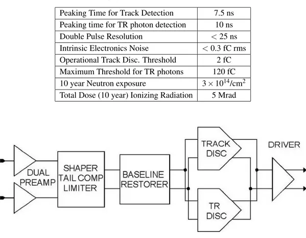
Table 1. Design goals for the TRT Front End electronics.
Peaking Time for Track Detection 7.5 ns Peaking time for TR photon detection 10 ns
Double Pulse Resolution < 25 ns
Intrinsic Electronics Noise < 0.3 fC rms
Operational Track Disc. Threshold 2 fC
Maximum Threshold for TR photons 120 fC
10 year Neutron exposure 3 × 10¹⁴/cm2
Total Dose (10 year) Ionizing Radiation 5 Mrad
Figure 2. Block Diagram of one channel of the ASDBLR
to give a trigger point based on a signal significantly higher than the intrinsic and systematic noise. Transition Radiation (TR) photons created by energetic electrons transiting layers of polypropylene radiator placed between the straws are stopped primarily by xenon atoms in the gas mixture. This high Z inert gas allows efficient absorption of TR photons whose energy is in the range of 5-15 keV, well above the typical 2 keV deposited by a minimum ionizing track. Extending the peaking time of the TR photon detection circuit to 10 ns allows integration of the direct and reflected signal from the far end of the unterminated 0.5–0.7 m straw. The extended peaking time reduces the variation in amplitude versus position of the avalanche along the straw [3]. The basic design goals for the ATLAS TRT Front End electronics are summarized in table 1.
1.3 Description of the ASDBLR
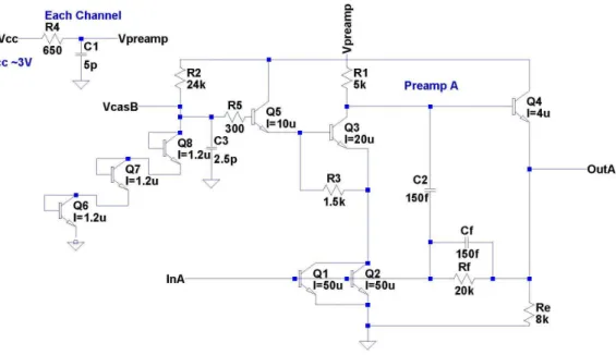
The ASDBLR consumes about 40 mW per channel and provides the complete analog signal pro-cessing chain for eight straw tubes from straw anode input to a three level digital output that signals arrival of the earliest ions at the wire with one level and the presence of a signal compatible with a transition radiation photon for the other level.
Figure 2 shows the signal processing blocks: Dual Preamp, Shaper, Baseline Restorer, High and Low level discriminator and driver. This largely differential design depends on good device
2008 JINST 3 P06007
Figure 3. Schematic of one of the two matched preamps used per channel.
matching rather than the absolute values of circuit elements in this DMILL process. The differential nature of the design also has the benefit of providing a rate independent power consumption. 1.3.1 Dual preamp
The dual cascoded common emitter preamp shown in figure3 is optimized for low-noise and radi-ation resistance. The duplicate circuits are interleaved in the layout to equalize topological effects and provide the best DC-balanced output to the differential shaper stage. The common emitter inputs are self-biasing at approximately +750mV. Since the preamp input is directly coupled to the wire, the common emitter input sets the anode potential. Anode current from the avalanche pro-cess flows directly into the preamp input. At high rate operation the average straw anode current is as high as 10 µA but does not significantly affect the operation of the circuit. The gain of the preamp is 1.5 mV/fC with a peaking time of 1.5 ns for an impulse input. Both preamp inputs for each channel are bonded out to package leads although only one input is attached to the straw wire anode. The second preamp input offers an important benefit in helping control channel-to-channel pickup external to the chip and reduces sensitivity to common-mode signals.
Significant attention was given to the protection of the preamp input since the input is directly attached to the straw anode wire. A breakdown or spark discharge in the straw sensor shorts the anode with the cathode which is held at a large negative voltage. Such a breakdown discharges significant current into the preamp input. To protect the input a fast response input protection diode was designed into the ASDBLR using the normally reverse biased collector-base junction of an array of large, single stripe, NPN transistors. The protection device on the preamp input that is attached to the wire is significantly larger than that on the other, typically unused, input. The “unused” input can be (and is in the board designs discussed in section 3) attached to a board level trace to help balance the common mode charge injection in the interconnect between the straw and the preamp. A total of 380 µm of emitter length provides 0.5 mJ breakdown protection when a
2008 JINST 3 P06007
series 24 Ohm resistor is used between this input and the wire. This external resistor contributes 8% of the total intrinsic noise at the track comparator input. Nevertheless, this on-chip breakdown protection is not entirely sufficient so an external diode (BAW56) is mounted on the Front End boards in parallel with the ASDBLR protection diode to fully guarantee the inputs.
In low-noise amplifier designs, the input transistor is the most significant source of additional noise from thermal noise due to unavoidable resistance in the base and from the statistics of tran-sistor current. Usually the technology dependent base resistance noise is ameliorated by increasing the size of the input transistor, but this results in reduced current density for a given power dissi-pation. Radiation studies (see section1.7) of the DMILL transistors have shown that in the high radiation environment of the ATLAS detector the minimum acceptable current density is 5 µA/µm of emitter length. At smaller values of current density, the gain of the transistor after ten years of ATLAS operation falls about an order of magnitude from its original value to ∼20-30.
The preamp is the part of the circuit most affected by the loss of transistor gain but will still maintain acceptable performance down to a beta of 30. Noise optimization showed that a collector current of 700 µA is a reasonable tradeoff between low power consumption and low intrinsic noise in the input transistor. This optimization sets the size of the input transistor to approximately 100 µ m. Each input transistor is realized as two physical transistors in parallel which allows the layout of the dual preamp to use a cross quad configuration. This cross quad helps to match the thermal and topological environment of the two preamps.
The dominant pole of the preamp is created by an 300 fF feedback capacitance in parallel with the 20 kΩ feedback resistor. These components help minimize noise and create a 275 Ohm input impedance that is well matched to the straw characteristic impedance of 295 Ohms3 and that is reasonably independent of frequency. The dynamic range of the preamp is greater than 600 fC making it the last stage to saturate from large signal depositions in the straw. The total preamp current per channel is about 2.4 mA.
1.3.2 Shaping stages
The differential three-stage shaper and preamp together provide four equivalent 1.25 ns poles of shaping to produce a nearly symmetric response with 5 ns peaking time for an impulse ionization input. The first shaper stage converts the dual preamp output to a differential signal with a gain of two. The second stage provides ion tail cancellation for either xenon or more conventional argon-based gases, as selected externally. A full scale range of 600 fC allows the tail cancellation to be effective over the widest feasible range of charge depositions. The final shaping stage contains a pole-zero network that cancels the short tail added by preamp feedback components and limits the maximum output response of the shaper to 140 fC equivalent input, the largest expected threshold setting for the TR discriminator.
1.3.3 Baseline restorer
The differential signal from the shaper is AC-coupled through 8 pF capacitors into the baseline restorer (BLR) where a bridge diode network with dynamic current control (figure 4) provides a 3Note that the anode wire resistance of about 80 Ω/m must also be taken into account in understanding the signal propagation.
2008 JINST 3 P06007
Figure 4. Baseline restorer functional schematic.
variable impedance shunt across the AC coupled differential signal. Current in the bridge deter-mines the shunt impedance and is dependent on the polarity of the differential output. The shunt impedance increases as signals of the desired polarity are passed to the next stage (discriminator), and decreases when the shaper output returns to baseline. Overshoot (due to discharge of the cou-pling capacitors) results in an increase in current in the bridge which lowers the shunt impedance across the outputs and quickly returns the signal to baseline.
1.3.4 High and low level discriminator
The BLR is followed by two independent discriminators, one with a low threshold level for track-ing, the other with a higher threshold for transition radiation (TR) detection. The low level discrim-inator contains additional integrations to increase the 5 ns peaking time of the shaper output to 7.5 ns and can reliably be set to trigger on signals between 1 and 10 fC. This discriminator is designed to mark the time of arrival of the avalanche signal from the earliest primary electrons liberated by an ionizing track. Since the primaries move at a predictable velocity, the time information can be used to designate the closest point of approach of the track to the wire. The high level transition radiation discriminator utilizes the same basic configuration, but has a 10 : 1 attenuation at its input and adds 5 ns to the shaping time for a shaping time of 10 ns. This longer time constant allows integration of the prompt and reflected straw signal for accurate energy discrimination of transition radiation photons.
1.3.5 Ternary driver
The low level and TR discriminators switch separate 200 µA currents between shared differential outputs to form a current sum of the combined discriminator outputs. This simple encoding scheme
2008 JINST 3 P06007
Table 2. ASDBLR Single Channel Ternary Encoded output.
Signal Detected Ternary Plus Ternary Minus
Below Low and High Threshold -200 µA 0 µA
Above Low Threshold -100 µA -100 µA
Above Low and High Threshold 0 µA -200 µA
shown in table2 is based on the assumption that the track discriminator output is always present when the TR discriminator is triggered due to its lower threshold [2].
1.4 Wafer fabrication
The ASDBLR was fabricated in a 0.8 µm minimum feature size, BiCMOS Silicon On Insulator (SOI) process. Two prototyping cycles allowed the understanding of issues of yield and substrate pickup that were not apparent from manufacturer provided information. Previous experience with several generations of similar analog wire chamber ASICS in fully commercial processes led to an expected a yield of 90% or greater. It was somewhat surprising to find that the yield was closer to 50 to 60% after folding in reasonable parametric limits on threshold. Measurement of test resistors on the fabricated wafers showed an unusually large number of devices whose absolute resistance varied by 20% or larger from the average value on the wafer. This variance was attributed to a high defect density in the process. Although there was no obvious circuit based way to eliminate this quality control problem it was possible to adjust the number of wafers purchased to accomodate this lower yield.
A second problem had to do with pickup between circuit blocks. Analog device models pro-vided by the manufacturer did not account for capacitance across the insulator layer to the back substrate leading to an observable difference between calculated and measured impulse response when the input capacitance was not balanced between the two inputs. Figure 4 shows a measure-ment on the first ASDBLR prototype at the analog monitor with and without balanced capacitance on the inputs. Once these were observed it was a relatively simple matter to revise the models, symmetrize the pickup and eliminate the harmonics. The final production of 141, six inch wafers with 1017 useable die per wafer took place in the second half of 2003.
1.5 ASDBLR packaging
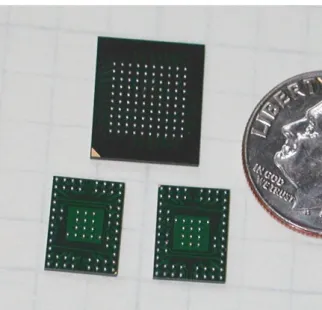
Geometric constraints of the TRT Barrel allow a space for each channel of only 30 mm2 on the surface normal to the direction of the wires. In addition there is less than 2 cm in distance along the direction of the wires. This tight constraint encouraged a search for a small footprint package for both the ASDBLR and the DTMROC. A custom Fine Pitch (0.8 mm) Ball Grid Array (FPBGA), shown in figure 6 was the most cost effective choice. Due to the relatively low lead count of the ASDBLR it was possible to depopulate part of the 0.8 mm2 grid near the inputs and outputs to improve the signal path and simplify the printed circuit board layout.
1.6 ASDBLR testing
Packaged ASDBLRs were delivered in 208 position JEDEC trays with laser engraved, 2-D bar coded, serial numbers. All chips were tested at the University of Pennsylvania Chip Testing Facility
2008 JINST 3 P06007
Figure 5. Response at the Shaper monitor output of the first DMILL prototype ASDBLR indicated a po-tential for harmonic ring when the capacitance at the inputs was not balanced (upper trace). In the lower trace the capacitance on one input was 22 pF and 7 pF on the other. The model parameters were modified to reflect these results and the second prototype and production devices show no harmonic ring.
Figure 6. Two ASDBLR and one DTMROC ASIC, in their custom FPGA packages are shown in comparison with a US dime for size comparison. The solder balls are 300 micrometers in diameter on an 800 micrometer grid.
- an 80 pin, 400 MHz, IMS MSTS chip tester fed by a custom adapted Exatron robotic chip handler. Each chip was DC tested for power supply currents, input channel resistance, output switching and output switching current. In addition, each channel was parametrically characterized for 50% efficiency thresholds using a test pulse injection at values of 0; 3; 5; 30; and 50 fC and the results were written into a mySQL database. Chip testing required slightly more than 30 seconds per chip including robotic handling from the tray to the test socket and back. More than two thirds of the available chips were tested before the selection criteria were finalized. Channel to channel matching at 3 and 30 fC test pulse proved the largest hit on final yield numbers of slightly better than 50%. After good chips were identified from the database, the same Exatron robot sorted good chips into trays that were sent on to board assemblers.
2008 JINST 3 P06007
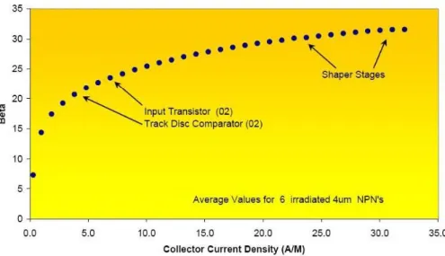
Figure 7. Measured single isolated DMILL SOI transistor current gain (Beta) prior to annealing but after 3.5 ×10¹⁴ neutrons per cm2as a function of current density in A/m. The arrows indicate approximate collector
current densities in various parts of the production ASDBLR circuit (Note that annealing at > 100oC for 24 hrs was found to improve the measured gain by a factor of 2.).
1.7 Radiation hardness
The ASDBLR relies on the characteristics of the DMILL NPN transistors, resistors and capacitors. The most sensitive parameter observed to change with radiation is the NPN transistor gain which is sensitive to displacement damage from exposure to neutrons and protons. Figure7 shows one of the preliminary measurements of the gain (Beta) of the SOI process NPN transistors as a function of current density after exposure to 3.5 × 10¹⁴n/cm2at the fast fission neutron source in Prospero, France. Although time efficient, exposure to a ten year accumulated dose in a few hours at a high rate facility is not a completely realistic test. It is well established that some gain recovery will take place over time due to self-annealing. An improvement of a factor of two in gain was measured after annealing the same transistors at > 100oC for 24 hrs. The results after annealing are generally believed to more realistically represent the expected result of low rate, long term exposure that the Front End electronics will actually experience. As can be seen in the plot the gain of the NPN transistors is a strong function of current density after exposure to neutrons. We chose to operate the preamp input transistor at a current density of 7 µA/m to minimize it’s gain loss. See Ref [4] for more details.
Radiation tests on production ASDBLRs have shown that the ASDBLR is capable of with-standing the predicted 3.5 × 10¹⁴ (1 MeV NIEL - Non Ionizing Energy Loss) neutrons/cm2and 7
Mrad ionizing radiation without significant loss of performance, although it has also been shown that unexpectedly high levels of thermal neutrons, in addition to the projected higher energy neu-tron dose, would compromise the useful lifetime of the ASDBLR [4]. The ASDBLR threshold input gives access to an on-chip transistor and, thus, a way to obtain a sensitive measurement of the change in NPN transistor gain after radiation damage. The threshold input is wired directly to the base of a 4 µm NPN transistor in each of the 8 channels. Measurement of the base current in those
2008 JINST 3 P06007
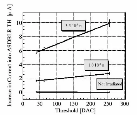
Figure 8. Measured change in ASDBLR threshold current versus DTMROC DAC setting (one DAC count = 5mV) after exposure to 3.5 × 10¹⁴n/cm21 MeV NIEL neutrons at the French Prospero facility and after annealing. Using the measured threshold current the worst case transistor gain was estimated to be 55 after neutron exposure and after annealing. The 20% variation from post annealing single transistor measurements is within the expected fabrication run to run variation.
threshold input transistors in conjunction with knowledge of the corresponding calculated collector current in those transistors allows a relatively accurate estimation of the ASDBLR current gain or beta (beta = Collector current/Base current). Figure8 shows the measured threshold current vs set-ting for production ASDBLR ASICS prior to and after exposure to a neutron source. It should be noted that the post exposure threshold measurements were taken after annealing for 24hrs at 100C. These results imply a transistor gain of 55 after exposure to to 3.5 × 10¹⁴n/cm2. Simulations show that the ASDBLR performance is threshold shifted but remains acceptable for values of transistor gain as low as 30.
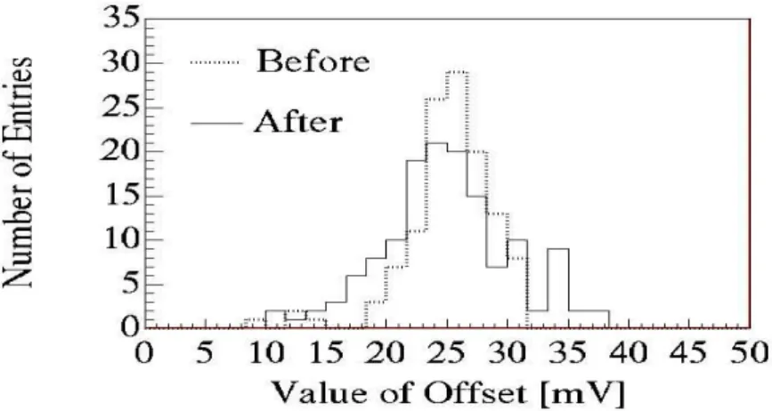
The DMILL NPN transistors in the ASDBLR show very little sensitivity to ionizing radiation at the doses expected after 10 years of operation at LHC. Figure 9 shows the channel by channel threshold offsets before and after exposure to 7 Mrad of Co60.
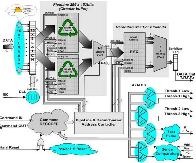
2. DTMROC
The complementary digital readout chip for the TRT is the Drift Time Measurement/Read Out Chip (DTMROC ). The initial prototype DTMROC [5] was produced in the same DMILL process as the ASDBLR but relatively low yields led to a redesign. The production chip [6] was implemented in a commercial 0.25 micron CMOS process and is designed to operate using the LHC 40 Mhz clock.
2008 JINST 3 P06007
Figure 9. The plot above shows the measured ASDBLR threshold offsets before and after exposure to 7 Mrad of Gamma radiation. A small amount of broadening is evident in the distribution plotted with the solid line.
A block diagram for the DTMROC is shown in figure10. We outline the functionality below and then describe each block in detail. Finally we provide performance information.
The DTMROC accepts 16 ternary inputs from two ASDBLRs, the analog Front End process-ing integrated circuit, described above. The ternary signal encodes time over threshold for the two separate discriminators on the ASDBLR. The low threshold signal is used for tracking and the DTMROC records it in 3.12 ns bins. The high level discriminator is sensitive to the presence of a transition radiation signal and the output of that high level discriminator is latched as a single bit during each 25 ns clock cycle that it is active.
The DTMROC has five differential LVDS connections to the Back End electronics: • BX — the 40 MHz LHC clock
• Reset — a hard reset
• Command In — trigger and control data input • Command Out — control data output
• Data Out — drift time data
BX, Reset, Command In, and Command Out are bussed to a group of DTMROC chips. Each DTMROC has a private Data Out line to the Back End electronics.
The DTMROC contains a programmable depth Level 1 pipeline to hold the front end data until the first level trigger arrives. When a trigger arrives as a serial string on the Command In line, the data (eight bits from the digitization of the low threshold input and a single bit from the state of high threshold input) for three successive bunch crossings are transferred to a derandomizing buffer. From the derandomizing buffer those 27 bits of data per channel are serialized and sent off chip over a low voltage differential signal (LVDS) twisted pair copper connection — Data Out. The data are preceded by a header giving the contents of a 3 bit trigger counter and a 4 bit clock counter. There is also a bit to indicate if the chip is in “SENDID mode,” in which case it sends its hardware address rather than the input data and a bit to indicate if any one of a number of error conditions is true — a total of 10 header bits.
2008 JINST 3 P06007
Figure 10. Overall block diagram of the DTMROC chip.
In addition to the main data path described above, the DTMROC Command Out port is used for reading back the contents of downloaded registers and of status registers. In addition, the Command Out port implements, an optional asynchronous wire-or output of the 16 low level outputs of ternary receivers for use in self triggered running.
The DTMROC also contains four 8 bit Digital to Analog Converters (DACs) to set the low and high thresholds on each of the two ASDBLRs to which the DTMROC is connected. There are also a pair of one bit digital outputs that are used to control the shaper of the ASDBLR.
A testpulse generator with programmable amplitude and timing is provided for testing and calibrating the ASDBLR. Four additional DACs and four comparators are available to measure the temperature and Vdd (+2.5V) on the DTMROC die as well as Vcc (+3V) and Vee (-3V) for the ASDBLR via two external connections. This array of DACs and comparators is referred to as VT-sense (Voltage/Temperature-Sense).
A Command Decoder provides register read and write functionality and well as general chip control and fast signal decoding. The Command Decoder receives commands over the Command In line and transmits readback data over the Command Out line.
2008 JINST 3 P06007
Table 3. Encoding function of the current in units “U” of current that are sourced from the DTMROC inputs into the ASDBLR outputs.
Amplified Signal in the ASDBLR True Signal Complementary Signal
No signal above thresholds 2U 0
Signal between low and high thresholds 1U 1U
Signal above both thresholds 0 2U
2.1 Analog blocks 2.1.1 Ternary receiver
The ASDBLR output is a constant total-current, differential ternary signal (0, 1 and 2 units as shown in table2.1.1) where a signal unit is 200 +100 / -40 µA. This current is pulled from the DTMROC Ternary Receiver inputs which sit at about +1.2 V and have an input impedance of about 200 Ohms. In this scheme, there is a constant return current flow through the negative ASDBLR supply to the analog and then digital grounds and then to the positive DTMROC supply. This non-zero return current produces a small DC offset between analog and digital grounds but obviates the need for a much more complex fully balanced output drive stage in the ASDBLR.
The ternary receivers convert the encoded currents back into two separate digital waveforms. Under quiescent conditions (no ASDBLR pulse) there is a current of 400µA leaving a TRUE input of the DTMROC. A pulse will be viewed as a rising voltage on the TRUE input.
The Ternary Receiver circuit is capable of accurately decoding tri-level differential current pulses as short as 4ns (at base). The circuit is based on differently ratioed differential current mirrors after the common gate current receiver. The use of ternary signals permits high-density communication between the ASDBLR and DTMROC chips without driving up pin-counts and without causing self-oscillations via large signal couplings back to amplifier inputs.
2.1.2 LVDS interface
The interfaces to the Back End electronics are all implemented as true LVDS differential signals. The BX, Reset and Command In input lines are received in standard high impedance differential receivers taken directly from the CERN-RAL library with a guaranteed sensitivity for signals of 25 mV differential or greater and minimum signal widths of about 5 ns.
The Data Out driver is a custom design based on standard LVDS topology with dual current sources driving an H bridge output. For the DTMROC Command Out driver to function on a multi-source Command Out bus it was necessary to include a tri-state function to turn off the current sources except when a particular chip was addressed. Given the need for the tri-state functionality, it was straightforward to include a secondary mode of operation for the Command Out driver where it can be used as a simple current drive into a distant summing node. By connecting the input of the Commmand Out driver to an OR of the 16 straw tracking signals, it is possible to treat the set of Command Outs on a given Front End board as a single current sum so that a distant comparator can act as a multiplicity trigger on any minimum number of simultaneous ternary inputs. This allows self-triggering for cosmic or source running and was used during some of the commissioning tests.
2008 JINST 3 P06007
2.1.3 Digital to analog converters
Four dual, eight-bit Digital to Analog Converter (DAC) blocks are used in the DTMROC to provide a total of four ASDBLR thresholds, two temperature — voltage monitor reference voltages and two Test Pulse Output References. Each dual DAC creates two eight bit reference voltages with a source impedance of 5 kOhms. Two eight bit switch arrays steer ratioed currents from current mirror slave devices to provide an eight bit current output into an internal 5 kOhm resistor. Current in the mirror master array is adjusted by an Opamp driver to provide an output voltage across an internal resistor (10 kOhm) that matches the internal band gap 1.25 V reference. The output of each DAC is a voltage in the range of 0 to 1.25 V with a least significant bit step of about 5 mV.
Two of the dual DACs are used to program thresholds for the ASDBLR chips associated with the DTMROC — two tracking thresholds and two transition radiation thresholds. The remaining two dual DACs are used to control test pulse amplitudes and measure on-chip temperature and voltage and two external voltages as explained in the next sections.
2.1.4 Testpulse generation
Each ASDBLR has two test inputs to couple an external test signal to an on-chip bus capacitively connected to each of four even or four odd ASDBLR preamp inputs. The DTMROC has a test pulse generator that provides a shaped signal to these ASDBLR test inputs. The DTMROC test signal is shaped as an integral of the expected point ionization signal in a TRT straw so that the differentiated signal at the ASDBLR preamp input closely follows the shape of a pulse from a Xe filled 4 mm straw.
Each test pulse generator is adjustable in amplitude (roughly 0 to 50 fC) and time (roughly 0 to 35 ns relative to the BX clock). A dual eight bit DAC (see above) controls the amplitude of the Odd and Even test pulse outputs although only the top six bits of the DACs are connected to the control register. An external connection (TPbias) can be used to adjust the output range — the nominal 0-50 fC range requires a 9 kOhm resistor between TPbias and 0V. The time delay of both Odd and Even outputs is controlled relative to BX through a single 32 position delay line, addressable via a five bit register field. There are separate enable bits for the Odd and Even test pulse outputs to simplify program control of the various test pulse sequences.
2.1.5 Temperature and voltage sense
A simple measuring scheme is used to monitor on-chip temperature, Vdd voltage, and two off chip sense inputs. A monitored voltage is compared to a programmed DAC value by a dual low offset voltage comparator. The comparator output value is stored in the Common Status Register and can be enabled as an input to the Error Bit. The DAC voltage range is limited to 1.25 V so the power supply voltages are scaled down suitably.
Two on-chip comparators are fed from one DAC output. These two comparators are attached to an external input via an on-chip or an external divider and to an internal current source feeding a temperature sensing diode. Two additional comparators are fed from a second DAC and compare that value to a second external voltage source and an internally divided copy of Vdd.
By sweeping the DAC setpoints it is possible to find the value of Vdd with a resolution of about 10 mV or the temperature with a resolution of about 2 degrees C given the 5 mV LSB of
2008 JINST 3 P06007
the DACs. By attaching the external voltage inputs of some DTMROCs on a board to the local ASDBLR Vcc or Vee power lines it is possible to monitor power supply and temperature values at each Front End board. Because the comparator outputs can be set as an input to the Error Bit, by properly enabling the error flags it is possible to learn of significant power or temperature changes in a few tens of microseconds.
2.2 Timing 2.2.1 DLL
The Delay Locked Loop (DLL) used in the DTMROC is a standard design with eight delay stages made with current starved inverters feeding back via the last inverter to a common point where there is a comparison with the incoming 40 MHz LHC clock. The control voltage for the starved inverters is then adjusted up or down depending upon the sign and magnitude of the phase error at the comparison point. This gives eight buffered clocks, BX0 to BX7 which are used to latch incoming straw data in 3.12 ns bins.
The DLL block also generates a nearly perfect 50% duty cycle clock waveform and this may be used as the clock signal throughout the DTMROC upon register selection. This internal clock, however, does not obviate the need for a stable 40 MHz external clock, it simply relaxes the duty cycle requirement somewhat on that clock.
As a diagnostic and monitoring tool, the DTMROC includes an eight bit latch for the BX0..BX7 signals that is updated each LHC clock cycle. A latch pattern showing a 50 ± 12.5% duty cycle results in a “DLL locked” bit set in the Common Status Register.
The DLL can be reset via the command decoder or via the external Reset line or upon power up. 2.2.2 Latch
The asynchronous data from the ASDBLR arrives as pulses with ranges in duration from ∼5 ns to many 25 ns clock cycles. For the low threshold (tracking) signal, the asynchronous data can simply be latched continuously by the BX0..BX7 clocks producing an ongoing bit stream record with 3.12 ns resolution or about 1 ns RMS. Each 25 ns clock cycle (eight of the 3.12 bins) is then recorded as an eight bit record in the Level 1 Pipeline memory. However, the high level threshold, because it only needs to be recorded as one bit per clock cycle, requires a synchronizing latch sensitive to transitions as short as 5 ns. Any high state during a given clock cycle is then stored in the Level 1 Pipeline as a high for the next clock cycle. In addition, a special “accumulate” mode has been implemented for this latch so that it does not reset each BX cycle as it would in normal data taking, but resets only upon external command. The accumulate mode is useful for chamber testing with radioactive sources or for looking at average noise rates.
2.3 Digital blocks 2.3.1 Pipeline
The Level 1 Pipeline is a logical FIFO block that stores the nine bits (one high threshold bit plus eight time digitization bits of the low threshold) of latched data from each input channel, the current value of a four bit clock counter plus a one bit error flag from the DLL. This FIFO is designed to hold the Front End data for the length of the Level 1 trigger latency.
2008 JINST 3 P06007
The pipeline is implemented as two banks of 128 deep by 153 bit wide Random Access Mem-ory (RAM) built out of 34 blocks of 128x9 bit memMem-ory cells - a CERN library part. The pipeline operates as a continuously running circular buffer, updating the read and write pointers into the memory. Writes (and therefore reads) alternate between the two banks of RAM to minimize power consumption fluctuations that could occur on parallel access to all memory blocks. The memory controller also implements a Built In Self Test (BIST) function to allow thorough memory tests without massive I/O traffic.
2.3.2 Derandomizer
The Derandomizer is an additional buffer also acting as a FIFO built from the same synchronous dual-port static RAM memory as the Pipeline, but with half the number of banks giving a storage capacity of 128 words of 153 bits. Upon receipt of a Level One Accept (L1A) the current Pipeline output word and the following two consecutive words are stored in the Derandomizer for readout. In addition to these data, the SENDID status bit, the L1ID and the Common Error status bit are stored. This gives 441 bits to be stored per event. The Derandomizer can store 42 events. In the case of memory overflow control logic provides a “full” flag and skips complete events avoiding synchronisation problems until the memory clears an event and is able to store a subsequent event. The Derandomizer and Pipeline SRAM blocks are equipped with Build-In-Self-Test (BIST) con-trolled via the Configuration register. The BIST result can be read out from the General Status register.
2.3.3 Serializer
As soon as the Derandomizer has any content, data is placed serially on the DataOut line at a 40MHz bit rate. Given the known constant event size it is possible to use a simple protocol with a three bit preamble “101” sent at the beginning of each event. When idle, the data output signal is “0”.
2.3.4 Command decoder
The command decoder block receives LVDS BX and a CommandIn signals from the TTC. The command decoder examines the CommandIn stream bit by bit and issues all the necessary timing signals (L1A,. . . ), internal registers read/write strobes and data. As implemented the decoding algorithm is very simple and is built from a shift register, a look-up table with valid command codes and comparator logic. This architecture is, in this case, lower cost in power and resources than a finite state machine. In order to insure that the circuit is robust against single event upset, additional logic was incorporated. The decoder for the critical ‘fast’ commands (L1A, SoftReset and BunchCrossingReset) and the command length counter were implemented as three copies for automatic error correction. A “surveillance” counter was implemented to guarantee the Register Transfer Level (RTL) state coverage and to release any access lasting longer then 171 clock cycles. Upon a read request the command decoder serially transmits the contents of the selected register on the differential CommandOut line, three clock cycles after the last bit of the command,. This CommandOut line is common to multiple chips on a board and therefore has a ‘tri-state’ capability. A three bit preamble (‘101’) is used for each data transmission and the idle state of this line is “HiZ”. The chip address is defined by setting external pins.
2008 JINST 3 P06007
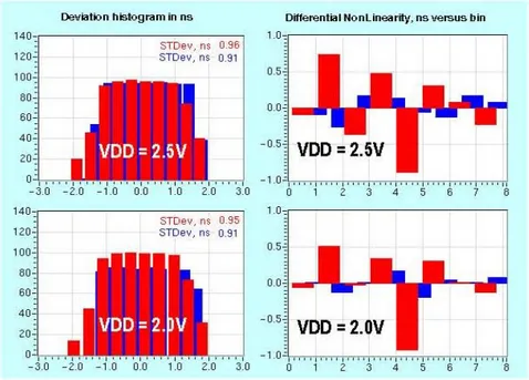
Figure 11. DTMROC’s time-measuring performance with the nominal 2.5 V and 2.0 V power supply. A 4.0 ns wide tracking pulse was injected at 100 ps intervals across three full clock periods, 75 ns in total. The picture shows the leading (red) and falling (blue) edges deviations from fit and differential non-linearity from a single channel.
2.3.5 Error handling
The implemented protocol is based on the ABCD chip specification [7], which lacks any advanced protection against transmission errors. The bit patterns for the commands are, however, chosen such that a single bit error should not cause the acceptance of a wrong command. An erroneous bit pattern in the middle of a command causes a flush of that unrecognized field and an attempt to decode the following command.
2.4 Measured performance
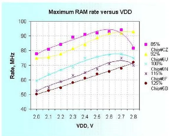
The preproduction fabrication of the design was fully successful and so the full production run of 48 wafers was done using the original masks which included lithographic adjustments to simulate two “faster” and two “slower” (from 85% to 125% of nominal propagation time) variations about nominal process parameters. The DTMROC preproduction tests looked at logical performance, time linearity, DAC linearity, and performance over voltage and process variations. As shown in figure 11, the time linearity is at the expected 1 ns level, differential and integral, not only at the nominal 2.5 V Vdd but also down to at least 2.0 V. The basic logic of the chip such as the command decoder, was shown to work properly at over 100 MHz at 2.0 V, but the RAM blocks did show some degradation at elevated clock speeds, lowered process speed and lowered supply voltage as shown in figure 12. As noted above, the RAM blocks can be tested with a built in self test routine as access through the DTMROC command structure is indirect and full coverage tests would be very time consuming.
2008 JINST 3 P06007
Figure 12. RAM access rate vs. Vdd and over various process variations. Note that for the DTMROC production run, the slowest (labeled 125% on this plot) process variation was not packaged.
Radiation tolerance was tested at the CEA Saclay Pagure facility up to 7 Mrad of Co60with the only degradation being about a 10% decrease in maximum DAC output voltage. SEU sensitivity was tested at the CERN PS irradiation facility using a 24 GeV proton beam with an integrated fluence of 1.8 × 10¹⁴p/cm2and shown to be of order 10−14cm2[8]. This rate of SEUs produces a per TRT error rate of much less than 1 Hz. The event counter reset signal is available at about 1 Hz and so the TRT can take advantage of ATLAS scheduled deadtimes to reset DTMROC chips that have suffered from SEU.
Production tests of the chips, conducted at the University of Pennsylvania Integrated Circuit Test Facility, concentrated on checking IDD, exercising the built in memory self test, and then
loading preset pulse patterns into the sixteen input channels and verifying proper time encoding within one LSB. The ternary receivers were checked for proper performance over their full range of amplitude and offset as were the LVDS I/O blocks. The DAC outputs and VT sense DACs were also exercised over their range and the test pulse output was checked at several values of amplitude and time delay. About 40,000 test vectors per chip were completed in about 30 seconds including robotic handling. All production chips were laser engraved with 2-D barcode serial numbers and test results were stored in a database. Chips passing all test criteria (about 85% yield) were pulled from the JEDEC trays and placed into final trays for the assembler by the same robot.
2008 JINST 3 P06007
3. Board designs
It is necessary to design the Front End boards, the detector grounding and shielding, and the power and signal connections to the outside world very carefully in order to achieve optimal performance. For instance, the 30 to 70 cm long straw tubes in the TRT are close to being ideal 1/4 wave antennas tuned to the ASDBLR peak bandwidth of about 33 MHz. In addition, the ASDBLR inputs must be carefully isolated from the 40 MHz digital logic of the DTMROC,
The geometry and other constraints of the TRT End Cap [9] and Barrel [10] are very different, therefore the designs of the End Cap and Barrel printed circuit boards need different optimizations. The basic schematic is, however, the same in each case — input protection (24Ω series resistor with a diode clamp to ground) at the detector and then the ASDBLR, DTMROC, and power filtering on the Front End boards. All signals in the system are differential except that the straw anode input is matched only pseudo-differentially by a trace carrying the ASDBLR dummy input as close to the detector as possible. The End Cap and Barrel printed circuit designs and justifications for the optimizations are discussed in detail below.
3.1 End cap boards
The End Cap straws are positioned radially, therefore while the 4 mm straws nearly touch with a center to center distance of 5.2 mm on the inner radius of the TRT, the straw to straw center distance along the φ direction is 8.2 mm at the outer radius where the electronics are located. This spacing allows almost 3/4 of a cm2per channel for the electronics located on the tread of the End Cap wheels. This location for the electronics, at the outer radius of the TRT up against the ATLAS solenoid cryostat, means that the radiation length of the electronics package is not as critical a concern as it is in the Barrel case where the electronics must be located at the end of the Barrel just before the End Cap. There is also, by design, sufficient room in r to allow separate, albeit closly packed, layers of printed circuit to handle the analog (ASDBLR) and digital (DTMROC) parts of the system.
3.1.1 ASDBLR boards
There are two schematically identical but physically different designs for the ASDBLR boards shown in figure 13 for the Type A and Type B End Cap Wheels. The Type B wheels are constructed with half the straw density in the Z direction of the Type A wheels. The Type A boards are about 60 mm square and serve 64 channels of detector (1/96 of a wheel in φ ) with eight ASDBLR chips. The Type B boards are about 120 mm in the Z direction to match the wheels. Both types are four layer, 1.5 mm thick, through-via designs. Connection to the straw anodes and cathodes is made via miniature connectors to the End Cap Wheel WEBs, complex rigid flex printed circuits that serve to attach the electronics boards to the detector both physically and electrically [9]. The high voltage decoupling capacitors for the cathode connections and 24 Ohm input protection resistors are mounted on the WEB as are the HV protection fuses which also serve as blocking or isolating resistors to the HV supply.
ASDBLR ternary outputs are sent to the DTMROC chips mounted on the Triplet Boards via four high compliance miniature connectors. ASDBLR control signals from the DTMROC and power for the ASDBLR chips also travel over these four connectors.
2008 JINST 3 P06007
Figure 13. Two A Wheel (l) and one B Wheel (r) ASDBLR boards top view showing the ASDBLR chips and the four multi-pin white connectors going to the Triplet Board described below. The semi-circular cutouts in the board edges are designed to clear plumbing and HV connections to the wheels.
3.1.2 DTMROC triplet boards
The Triplet boards are identical for Type A and Type B wheels. One Triplet board serves three ASDBLR boards — 32 Triplet boards per End Cap Wheel. Each Triplet board, shown in figure14, has 12 DTMROC chips and is constructed as three separate four-layer through-via printed circuits joined by flexible soldered on jumpers. The jumpers allow flexibility so that the Triplet can follow the curve of the End Cap Wheels. An initial design effort using rigid flex technology demonstrated good performance, but was abandoned because of cost considerations and because the stiffness of the flex circuitry was too great to allow easy assembly on the wheels.
3.1.3 Shielding
For the TRT End Cap, the Faraday shield around the straws is made complete through the WEB structure on one side of the wheel up through the ASDBLR board and down the opposite WEB as shown in figure 15. The analog ground plane of the ASDBLR board acts not only as the cathode connection and reference for the ASDBLR input but also as a part of the Faraday shield. As a secondary shield, it was learned that completing the connection of the digital ground plane of the Triplet boards with a low impedance phosphor bronze clip between the edge plated segments of the Triplet boards provided additional cross talk protection from the digital logic on the Triplet. A full external Faraday shield constructed at the level of the TRT cable trays surrounds the detector and electronics.
3.1.4 Power distribution
Power is brought to the Triplet via the same 60 pin connector that also carries the four control lines and the 12 data output lines. The +2.5V power for the DTMROCs is filtered at the 60 pin
2008 JINST 3 P06007
Figure 14. End Cap Triplet board showing the four DTMROC chips per segment with the power and data connector on the right. The four white jumpers between segments carry control and data signals and power and power returns. Note that the breakaway bars at top and bottom of the Triplet are removed after testing.
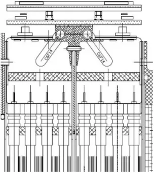
Figure 15. Cross-section drawing of the construction of an End Cap wheel. The DTMROC Triplet board is at the very top, then the ASDBLR board, the cooling structure and the WEBs.
connector, is returned via the digital ground plane on the triplet board, and is distributed only on the Triplet board. The ±3V power for the ASDBLRs is filtered to the analog return at the 60 pin connector and then distributed to the three ASDBLR boards. Analog and Digital power returns are commoned at the connector. Cooling is described in section4.2.
3.2 Barrel boards
2008 JINST 3 P06007
Figure 16. End-on view of the TRT Barrel during above ground testing at CERN before installation in the ATLAS detector hall. Each of the three types of quadrilateral modules (types 1,2, and 3 from inner to outere radius) is bisected by a member from the Barrel Support Structure. These six different triangluar shapes define the geometry of the Front End boards.
is a stringent radiation length limit as the boards must be situated in the middle of a tracking region. The available board area per straw is also about a factor of two less than in the End Cap case. The mounting of the Barrel modules in the Barrel Support Structure (BSS) defines a set of triangular spaces shown in figure16 into which the electronics must fit in order to connect to the anode and cathodes brought out on the module tension plates.
After exploring a number of possible design concepts all of which failed to meet the design constraints discussed below, the collaboration settled on a single board mounting both ASDBLR and DTMROC chips [11] as opposed to the two board solution used in the End Cap.
3.2.1 Design constraints
The connectors designed into the Barrel Tension Plates (individual sockets for 0.5 mm pins ar-ranged in groups of 16 anodes and 6 grounds) shown in figure 17 [10] are not suitable for simul-taneous mass insertion as would be required by a triangular printed circuit board serving from 10 to 27 of these 16 anode patterns. In addition, the areal electronics density required, especially in the smallest (Type 1) modules, is somewhat greater than practical. Therefore, an additional small
2008 JINST 3 P06007
Figure 17. Cross-section view of a barrel module tension and HV plate region. The Protection Board (labeled ‘Electronics Card’) is shown plugged into sockets in the tension plate. The active electronics plugs into a high density, high compliance connector on the protection board and is parallel to the Protection Board.
board, the Protection Board, was added to the scheme to allow a transition from the 0.5 mm pin connectors to the high compliance miniature connectors used on the End Cap — the protection board improves the mechanical compliance to allow, in the worst case, making 600 simultane-ous connections and provides a small additional surface area to hsimultane-ouse the clamp diodes and input protection resistors for the ASDBLR inputs.
The existence of a Protection Board coupled with the constraint that the overall depth in Z available for Barrel electronics including cooling and connectors is about 1.5 cm, a single substrate printed circuit solution becomes almost inevitable. Because of the obvious mechanical difficulties in using a liquid cooled plate under the ASDBLRs, a set of two piece machined Al plates were designed to be attached to the outer or DTMROC side of the triangle boards. In that way the cooling connections could inhabit space reserved for other plumbing connections.
3.2.2 Design rules
Although variations in geometry by end and by module layer require a total of 12 different board and cooling plate footprints, the design approach is the same for each. The basic rule is to separate the board into analog and digital domains splitting a total of 14 layers equally between them. Four levels of blind vias allow isolation of analog and digital signals within their separate domains. All fast signals are low level differential. Barrel boards are arranged in 16 channel ASIC triplets consisting of two eight channel ASDBLRs and one DTMROC. Analog connectors and ASDBLRs face inwards towards the barrel module. Two signal layers separated by an analog ground plane utilize short vias to isolate the inputs from the rest of the board. An empty layer below the input signal layers and a power layer with cutouts corresponding to the location of input signals minimize the capacitance to the other board layers. The analog side is enclosed by a second analog ground plane with a power layer finally facing outwards towards the digital side. The layer stackup is shown in figure18