COMPARISON EFFECT OF SPIN SPEEDS AND SUBSTRATE LAYERS ON
PROPERTIES OF DOUBLY DOPED TIN OXIDE THIN FILMS PREPARED BY
SOL-GEL SPIN COATING METHOD
A. BATTAL*,D. TATARa, A. KOCYIGITb, B. DUZGUNaFaculty of Education, Muş Alparslan University, 49100, Muş, Turkey
aKazım Karabekir Education Faculty, Atatürk University, 25070, Erzurum, Turkey bHealth Services Vocational High School, Igdir University, 76000, Igdir, Turkey
Tin oxide thin films doubly doped with antimony and fluorine (Sb, F) were deposited by sol-gel spin coating method at different spin speeds and substrate layers on glass substrate. Effect of spin speeds and substrate layers on the characterizations of the films was investigated. X-ray diffraction studies revealed that antimony and fluorine have been successfully doped into the SnO2 thin films and all the prepared films were single
crystalline in nature and exhibited orthorhombic structure with preferential orientation {021} family of planes. As the tin oxide thin films have quite often structure of tetragonal polycrystalline, this obtained orthorhombic structure is rarely in terms of literature. Although intensity of preferential orientation changed, its orientation did not change with increasing spin speeds and substrate layers. Also, peak intensity of the films prepared with 6 substrate layers was bigger than 5 substrate layers, but crystallinity in 5 substrate layers was better than 6 substrate layers. Transmittance (90-95%.) values found in this study were to be much better than previously reported values (50-80%). Together with these studies, PLQY value of an inorganic material such as tin oxide which weakly emit was measured. Eventually, the obtained results revealed that properties of the thin films were greatly affected by spin speeds and substrate layers.
(Received January 13, 2014; Accepted March 5, 2014)
Keywords: Doping, Crystal Structure, Spin Coating Deposition, Tin Oxide 1. Introduction
Transparent conducting oxides (TCOs) are widely used for several applications such as solar cell [1], heat shields [2], transparent conductor for optoelectronic devices [3], active channel materials for TFTs [4] and sensitive gas sensor [5-7] etc. and have extensively investigated owing to their marvelous properties [8-9]. Indium tin oxide (ITO) is the TCO material used as layer in most of optoelectronic applications. However, it is expensive and very low reserve. Hence, it is important to search and found a new material to replace ITO [10]. Tin oxide family is one of the metal oxide semiconductors suitable for use as TCO because of its excellent properties i.e. as an optical materials they have a high transmittance-reflectance in visible-near infrared region, as an electrical material they have a good electrical conductivity as n/p type semiconductor and a carrier mobility [11], as a chemical material they are amongst one of the few pure semiconductors [12], with low temperature (point of viewing thermal budget) film deposition properties and tailor making precursor [13-14] and high fabrication performance [15], as a mechanic materials they are also durable in acidic and basic environment, environmentally friendly, convenient for low vacuum depositions [16] and easy control of morphology and composition [17], as an commercial material they are cheap and abundant for large area with easy control of the doping level [18]. Hence, this tin oxide material is considered to be as settle as TCOs in all sorts of applications. In addition, the behaviors of these films greatly depend on deposition methods [19]. These films can
be employed by using many different methods such as thermal evaporation [20], sputtering [21] and spray pyrolysis [22]. Each of these methods has its own advantages and disadvantages. Sol-gel method does not need vacuum and allows for the fine control of the product’s chemical composition as well as porous microstructure [23], increased capability to tailor complex compositions, simple and economical in technological equipment, low thermal budget necessary for oxide film consolidation and specific controlled porosity properties [24-25]. Sol-gel spin coating method has been predominantly used in many attempts [26-38]. Recently, strong efforts have been made to develop metal oxide semiconductor materials with active optoelectronic properties such as photoluminescence properties, which may lead to new optoelectronic devices with superior performance [39-40]. Although more films produced by using sol-gel spin coating method have been reported by many people, to our knowledge, there is not yet more information about this method, doubly doped and effect of different spin speed and substrate layer on physical properties of doubly doped tin oxide thin films deposited by this method. Moreover, more report has not been declared about PLQY of inorganic material solutions. In this report, we have chosen the sol-gel spin coating method and fabricated on a glass substrate by this method. Detailed investigations about effect of spin speeds and substrate layers on properties of doubly doped tin oxide thin films prepared were conducted.
2. Experimental
2.1. Sol-gel Spin Coating Process
Sol-gel spin coating has been used decades long to deposit thin films. A spin process involves depositing a small material put on the center of a substrate and then to be spin the substrate. Centripetal acceleration causes the material to spread onto the surface of substrate. The properties regarding material (viscosity, drying rate, percent solids, surface tension, etc.) and spin parameters (spin speed, acceleration and time etc.) impact film properties. Spin parameters vary mostly for different materials and substrates. So, there is no fixed rule. Spin coating system is a cheap and easy method but specific problems can sometimes be formed such as too thin or too thick film formations, air bubbles on wafer surface, comets, and center circle like chuck etc. [41].
2.2 Deposition of SnO2:Sb:F/AFTO thin films
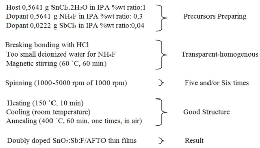
In this work, doubly (antimony (Sb) and fluorine (F)) doped tin oxide thin films (called SnO2:Sb:F/AFTO) were prepared by the sol-gel spin coating method on optical glass. Starter materials (precursors) of Sn, F and Sb elements, respectively are SnCl2.2H2O, NH4F, SbCl3 (from Merck Company). Concentration of solvent (0,05 M) in all experiment and doping weight ratio of Sb (2 4 olmalı%) and F (30%) are fixed. Firstly, optical glass substrates were cleaned in ultrasonic cleaner machine with Acetone-Isopropyl Alcohol-Acetone and Deionized Water, respectively, for 8 min and finally dried with nitrogen. Then, precursors were dissolved in the isopropanol solvent and few drops of HCl were added to break polymer binding. After dissolving, solution was stirred at 60 ˚C for 60 min to get a transparent sol. The sol was used to deposit thin films. The substrates were placed on the sample holder and spin speeds were applied ranging from 1000-5000 rpm in steps of 1000 rpm with number of substrate layers is fixed at 5 and 6 substrate layers, respectively. Deposition procedure was seen in Fig. 1 for doubly doped tin oxide (SnO2:Sb:F/AFTO) thin films deposited by sol-gel spin coating.
Fig. 1. Deposition procedure for doubly doped tin oxide (SnO2:Sb:F/AFTO) thin films
prepared by sol-gel spin coating
The spin cycle followed in this study was a two-step process: the first step was spinning for 10 second and at 500 rpm, the second step was spinning fastly for 20 seconds. The first step in this method enables to paste the sols substrates before starting the high speed next step is to make fluid thinner. After the successful deposition with 5 and 6 substrate layers, the coated substrates were heated by a two-stage heat treatment; the first one was in oven at 150 ˚C 10 min and the second one was in furnace at 400 ˚C for 60 minutes in air to remove the solvents from the substrate. Spin Coater system was purchased from Laurell Company (WS650Mz-23NPP-12000 rpm).
2.2 Thin film characterization and measurements
All experiments were carried out under approximately similar laboratory conditions. Structural, optical and electroactive properties of the thin films were characterized. For the structural characterization of these films was performed by using X-ray diffraction (XRD) measurements using a Rigaku D/Max-IIIC diffractometer with CuKα radiation (λ=1.5418 Å), at 30 kV, 10 mA. Transmittance measurements were obtained using a UV-VIS spectrophotometer (Perkin Elmer, Lambda 35). Jobin Yvon Horiba Spex Fluoromax-3 Spectrometer was used to measure the luminescence measurements. Quantum yields were determined in chlorobenzene in comparison with a standard DPA = 0,77. Excitation wavelength is 300 nm in all PL experiments.
3. Results and discussion 3.1. Structural properties
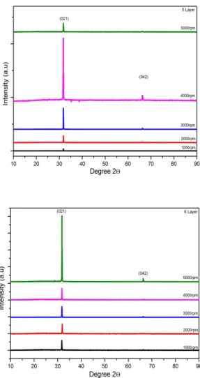
The XRD patterns of as-deposited thin films at different spin speeds with 5 and 6 substrate layers were shown in Fig. 2.
Fig. 2. XRD patterns of doubly doped tin oxide (SnO2:Sb:F/AFTO) thin films prepared
at different spin speeds with 5 and 6 substrate layers
All the samples deposited on glass were single crystalline with orthorhombic structure and highly oriented preferentially along (021) and (042) planes in nature. The intensity of (021) peak was stronger than (042). The diffraction peaks were indexed based on the orthorhombic SnO2 structure (Standard JCPDS Card No: 78-1063 Quality C). No other peaks are observed. These XRD results are rather original, because they are rarely found in the literature [42]. The crystal structure of SnO2 in all cases was, however, orthorhombic. Studies, until now, about the tin oxide deposited by spin coating indicated that the SnO2 thin film has very poor crystalline nature and the diffraction lines are assigned well to the tetragonal polycrystalline structure [1,2,7,40,43,44,55] etc. However, when the doping ratio and the deposition method were changed like in this work, single crystallinity with orthorhombic structure was newly formed. A similar result regarding orthorhombic structure has been observed for SnO2 films on various YSZ substrates by plasma enhanced atomic layer deposition [45]. X-ray patterns of produced tin oxide based films grown on the substrates at different spin speeds with 5 and 6 substrate layers revealed that good crystalline films were not formed at low rpms but high rpms gave good crystalline films. However, the XRD patterns were obtained for all deposition times. The intensity of preferential orientation increased with increasing spin speeds and substrate layers in all deposition times. Therefore, it can be said the intensity of peaks in 6 substrate layers is bigger than 5 substrate layers for best crystalline spin speed, but its orientation did not change with increasing spin speed and substrate layer.
In addition to XRD patterns, among the studied films was observed the crystallinity for 5 substrate layers was seemed to have a good crystallite than 6 substrate layers in all the
experimental conditions. When spin speed increased, crystallinity of all films was well compared to lower rpms which they bring about amorphous structure in crystalline structure of thin film. The thin films as-deposited at 4000 rpm and 5000 rpm with 5 and 6 substrate layers, respectively, showed the best crystallinity. We believed that further increases in rpm resulted in the crystallinity beginning to not good. The reason of this badly structure is that there is not enough material which made crystal owing to extreme speed. The high intensity of the peak (021) suggests that the thin films mainly consist of the crystalline phase [42]. At 4000 rpm, the intensity of the peak (021) for 5 substrate layers was higher than 6 layers. Because, 4000 rpm was enough to be form a thin film and an optimize spin sped for 5 layer rather than 6 layer which have a nonsufficient speed. But, at 5000 rpm, intensity of that peak for 6 substrate layers was higher than 5 layers. Because, that rpm was also enough to be form a thin film and an optimize spin sped for 6 layer rather than 5 layer which have thick layer. Therefore, we can conclude with certainty that spin parameters impact thin film structure.
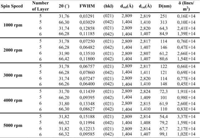
In general, analyses of all X-ray diffraction patterns, they demonstrated that antimony and fluorine have been successfully doped into the SnO2 thin films. Shortly, if the spin speed is too high, the solution will not stay on the surface and will spread out of the film during the spin off process whereas if the speed is too low the solution will not reach to the boundaries of the thin film leaving behind the un-deposited areas on the film. Similarly if the spin time is very short the film will be very thick and solution will also not reach to the boundaries of the substrate. However if the spin time is very high it will also have a negative impact on film morphology. There must be a balance between spin speed, acceleration and spin time [34]. The grain sizes for these films deposited at different spin speeds with 5 and 6 substrate layers were calculated using Scherer’s formula [46]; D =0.9λ/(β cosθ); where D is the size of the crystallite, β is the broadening of diffraction line measured at half its maximum intensity in radians (FWHM) and λ is the wavelength of X-rays (λ = 1.5418 Å). Values regarding structural of the films which calculated by using above equation are seen in Table 1 for (021) and (042) planes, respectively.
Table 1. Structural values of doubly doped tin oxide (SnO2:Sb:F/AFTO) thin films
prepared at different spin speeds and substrate layers
Spin Speed Number
of Layer 2θ (˚) FWHM (hkl) dstd(Å) dcal(Å) D(nm) δ (lines/ m2) 1000 rpm 5 5 6 6 31,76 66,30 31,74 66,28 0,03291 0,03029 0,12858 0,11185 (021) (042) (021) (042) 2,809 1,404 2,809 1,404 2,819 1,410 2,820 1,407 251 313 64,3 84,9 0,16E+14 0,10E+14 2,41E+14 1,39E+14 2000 rpm 5 5 6 6 31,78 66,28 31,90 66,42 0,07250 0,06482 0,13510 0,11800 (021) (042) (021) (042) 2,809 1,404 2,809 1,404 2,817 1,407 2,807 1,407 114 146 61,2 80,6 0,76E+14 0,47E+14 2,66E+14 1,54E+14 3000 rpm 5 5 6 6 31,78 66,28 31,74 66,26 0,06757 0,07860 0,07247 0,06400 (021) (042) (021) (042) 2,809 1,404 2,809 1,404 2,817 1,411 2,820 1,410 122 121 114 148 0,66E+14 0,69E+14 0,77E+14 0,45E+14 4000 rpm 5 5 6 6 31,70 66,20 31,80 66,30 0,11439 0,09395 0,13348 0,08627 (021) (042) (021) (042) 2,809 1,404 2,809 1,404 2,824 1,409 2,815 1,410 72,3 101 61,9 110 1,91E+14 0,98E+14 2,60E+14 0,83E+14 5000 rpm 5 5 6 6 31,82 66,32 31,82 66,32 0,15188 0,11994 0,12213 0,09585 (021) (042) (021) (042) 2,809 1,404 2,809 1,404 2,814 1,408 2,814 1,407 54,4 79,2 67,7 99,1 3,37E+14 1,59E+14 2,17E+14 1,02E+14 2θ-The Diffraction angle, FWHM - Full width half maximum, (hkl) miller indices,
For 5 substrate layers, the grain sizes of the films changed randomly with the increasing spin speeds until 4000 rpm and reached 72,3 nm at 4000 rpm then decreased. For 6 substrate layers, the grain sizes of the films were very nearly stable from 1000 rpm to 5000 rpm. Generally, this dispersing in grain sizes of the films was random and indicated that grain sizes of these films depend on spin speed and substrate layer. Regarding all the studied experimental condition, the results are associated with XRD patterns which show that grain size of the films in 5 substrate layers was seemed bigger than 6 substrate layers due to the films of very high quality in terms of crystallinity.
We can conclude with certainty that when we increased substrate layer, grain size of the best crystalline films in 5 substrate layers was larger than 6 substrate layers. This state continued for every spin speeds and substrate layers not including 5000 rpm. Also, in this report, dislocation density (δ) was determined using δ=1/D2 [47]; where D is the size of the crystallite like Table 1. The (δ) is defined as the length of dislocation lines per unit volume due to the fact that the (δ) is amount of defects in a crystal. It was concluded that when we increased substrate layer, dislocation density was increased. The small values of δ obtained in the present study confirmed the good crystallinity of the doubly doped tin oxide films deposited by spin coating [42,48]. The results are associated with XRD patterns which show that dislocation density of the thin films prepared with 5 substrate layers was smaller than 6 substrate layers owing to the films of very high quality in terms of crystallinity. Therefore, the growth mechanism involving dislocation is importance state and also dislocations in a crystal are imperfect associated with the mis-registry of the lattice in one part of the crystal with respect to the other parts [49]. The interplaner distance (d) for every crystal calculated from XRD results by using Bragg's law (n=2dSin). This d values were given in Table 1 are compatible with standard d values in JCPDS Card No: 78-1063 Quality C and were almost similar for the films with both 5 and 6 substrate layers. Moreover, value of full width at half maximum (FWHM) in XRD crystalline peaks for 5 substrate layers were found to be smaller than 6 substrate layers.
3.2. Optical properties 3.2.1. Transmittance
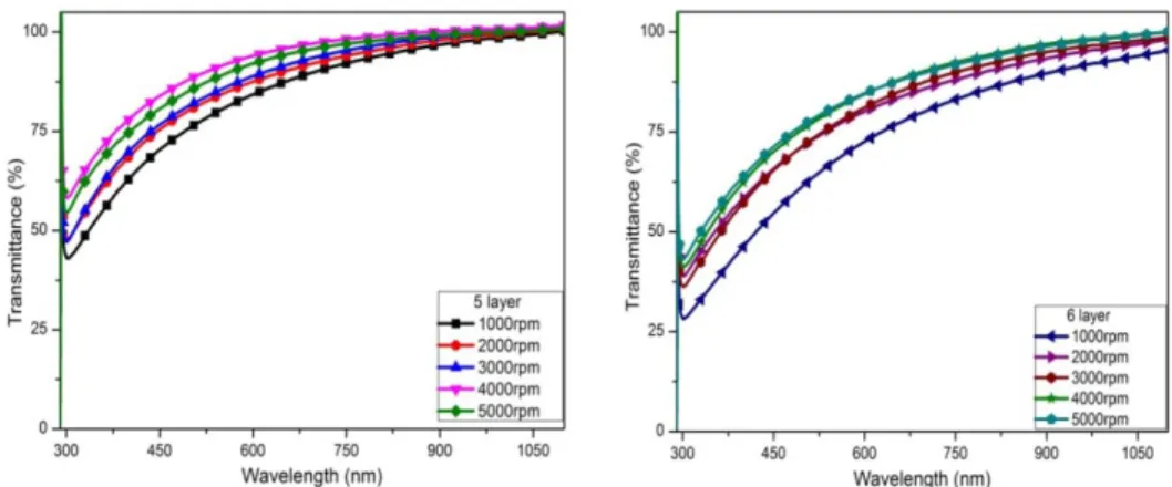
As it was shown in Fig. 3., the optical transmittance (T) properties of the thin films prepared at different spin speeds with 5 and 6 substrate layers have been characterized by UV-VIS spectrophotometer (Perkin Elmer, Lambda 35).
Fig. 3. Transmittance spectrum of doubly doped tin oxide (SnO2:Sb:F/AFTO) thin films
prepared at different spin speeds and substrate layers
The optical transmittance (T) was investigated using the transmission spectra in the wavelength range of 300-1100 nm. It has been found to be changing from 83% to 97% and 80% to 94% in the visible region depending on the spin speeds for 5 and 6 substrate layers, respectively.
Also, the value of transmittance at 900 nm is calculated about 90%. The values are comparable with literature [1-2,42,50].The highest transmittance was seen at 4000 rpm for 5 substrate layers and at 5000 rpm for 6 substrate layers. For both substrate layers, it increased with increasing spin speeds but decreased with increasing substrate layer.
In other words, when we increased substrate layer from 5 to 6, transmission of thin films with the best crystalline was decreased because of there are more materials on substrate as to lower substrate layer. When spin speeds increased, as can be seen from Fig. 3., the transmission values of the thin films changed from 90,00% to 97,20% then 95,84% for 5 substrate layers, from 80,14% to 90,48% for 6 substrate layers. These results are associated with XRD patterns. Already, since the thickness of the films decrease with increasing spin speed [34], transmittance automatically begins increasing. Regarding all the studied experimental condition, T values of the thin films prepared at different spin speeds with 5 substrate layers were found to be bigger than 6 substrate layers. It was concluded that good crystallinity give rise to good transmittance. Also, transmittances of AFTO thin films which prepared with this sol-gel spin coating are highest compared to the ones prepared with the other systems [37].
We successfully coated and obtained the films with good transparency as to the literature [42], though it is quite difficult to deposit doubly doped tin oxide (SnO2:Sb:F/AFTO) thin films with this method. Finally, the previous studies regarding tin oxide films prepared by sol-gel spin coating indicated that their transmittance value is about 50-80% [1,2,7,40,43,44,55] etc. But, in this report, the transmittance was found to be much better than the previous values and increased to 90-95%. Also, sample coloration as-prepared by spray pyrolysis [51] appear generally a bluish, but in this work a white fog was found for the first time [1,2,7,40].
3.2.2. Band gap energy
The fundamental absorption refers to band-to-band transitions, i.e. to the excitation of an electron from the valence band to the conduction band. The fundamental absorption, which manifests itself by a rapid rise in absorption, can be used to determine the band gap of materials [52]. The absorption coefficient (α) can be calculated from the transmittance (T) values which at the absorption edge in the transmittance spectra from the Lambert’s law α=ln[(1/T)/t] [53]. The variation of absorption coefficient against photon energy (hν) has the form of (the optical band gap of the films is found using the Tauc’s relation [48]) α=A(hν - Eg)n/2 where E
g is the band gap energy, A is a constant related to the effective masses associated with the bands and n is a constant and one for a direct-gap and two for an indirect-gap [54]. To determine whether the doubly doped TO films direct or indirect band gap, (αhν)2 vs. (hν) and (αhν)1/2 vs. (hν) plots were drawn. Since better linearity was obtained in the (αhν)2 vs. (hν) plots, the direct band gap values were determined by extrapolating the linear portion of these plots to the energy axis (zero absorption).
The Eg values are also calculated using the dT/dλ vs λ plots [55]. Eg values of the thin films as-prepared at different spin speeds with substrate layer were investigated using the absorption spectra. The values of direct band gap were estimated from the extrapolation of the linear portion of the curve to zero absorption and found to be in the range 3,12-3,46 eV and 3,18-3,41 eV for 5 and 6 substrate layers, respectively, depending spin speeds. The highest Eg value for the AFTO thin film that deposited was found at 4000 rpm and 5000 rpm for 5 and 6 substrate layers, respectively. It was concluded that when we increased substrate layer from 6 to 5, Eg was decreased. In this work, Eg values which compatible with the literature [54, 56] changed a little bit for different spin speeds. Eg values of the thin films prepared at different spin speeds for 5 substrate layers at same spin speeds was usually found to be bigger than for 6 substrate layers.
The annealing process may be supposed to decrease quantity of defects/dislocations and to get better crystal orientation. Because once film quality increases, Eg value increases due to decreasing band defects like reported by [57]. Hence, it was found that Eg value of the films up to the best crystalline rpm for was be wider randomly with increasing spin speeds and then it decreased slowly. In result, the non-radiative recombination reduced and the intensity of the blue/violet peak increased. The optical transmittances and the estimated Eg values were summarized in Table 2.
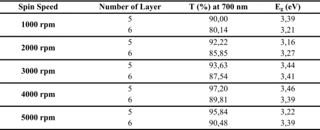
Table 2. Optical transmittance and the estimated Eg values of doubly doped tin
oxide (SnO2:Sb:F/AFTO) thin films prepared at different spin speeds
Spin Speed Number of Layer T (%) at 700 nm Eg (eV)
1000 rpm 5 6 90,00 80,14 3,39 3,21 2000 rpm 5 6 92,22 85,85 3,16 3,27 3000 rpm 5 6 93,63 87,54 3,44 3,41 4000 rpm 5 6 97,20 89,81 3,46 3,39 5000 rpm 5 6 95,84 90,48 3,22 3,39 T: Transmittance and Eg: Band gap energy
3.3. Luminescent properties
Photoluminescence (PL) measurements (excitation wavelength: 300nm) were carried out at room temperature by Jobin Yvon Horiba Spex Fluoromax-3 Spectrometer. It was studied effect of spin speed and substrate layer on the film PL and since PL spectra not only show the quality of films obtained but also give an information to us about defects in crystal [58], was investigated circumstances of defect states. Fig. 4 showed that PL spectrums (with range of 310–500 nm) of the thin films prepared at different spin speeds with 5 and 6 substrate layers, respectively.
Fig. 4. PL spectrums of doubly doped tin oxide (SnO2:Sb:F/AFTO) thin films prepared
at different spin speeds with 5 and 6 substrate layers
Excitation wavelength, 300nm, cannot be seen because scan area began from 310 nm in PL spectrum. It was observed that one broad emission peaks at approximately 347 nm (3,57 eV) and two small emissions at 398 nm (3,16 eV) and 469 nm (2,65 eV), respectively.
Origin of this broad peak is exciton emission which is originated from the recombination of the exciton corresponding to the near-band gap emission (NBE) inside tin oxide structure [59]. The intensity of NBE band peak is varied by spin speeds and substrate layers value. The origin of the peak at 398 nm is attributed to the electron transition from the donor level formed by oxygen vacancies or Sb+5 or F- ions to the acceptor level formed by the Sb+3 ions [60]. In deposited
polycrystalline oxides, oxygen vacancies are known to be the most common defects and form the donor level [61]. Some researchers found that SnO2 thin films exhibited a broad dominant peak near 396 nm (about 3.14 eV), which has been assigned to all the luminescent centers, such as nanocrystals and defects in the film [62]. Another peak observed at 469 nm, which corresponds frequently to blue luminescence and can be attributed to singly charged oxygen vacancies or luminescent centers in the films [63] indicating that these films contain a large number of defects.
It was concluded from PL measurements that peak positions of the films exhibit similar characteristic both at 5 and 6 substrate layers. But, intensity of the peak was found that films at 5 substrate layers to be much more generally than at 6 substrate layers, as films at 5 substrate layers had a good crystalline. And, if spin speed increased from low speed to fast, crystallinity was going to good and orientation preferentially improved (see XRD results). Meanwhile, as defect decreased (see Eg results in Table 2), intensity of PL spectra increased automatically. However, emission spectra shifted little bit to a UV region, when spin speed increased. Because, the spectral shift towards the UV region may be attributed to the improved crystallinity and a higher concentration of carriers [64]. Furthermore, the fundamental absorption edge is shifted toward the shorter wavelength side with the widening of the energy gap in the films may arise from a Moss–Burstein shift [65]. When spin speed and substrate layer increased, the grain size of the thin films became larger (see) and oxygen vacancies which related to luminescence intensity decreased (not shown here) [66]. So, PL properties of the doubly doped tin oxide thin films are dependent on the preparation conditions such as spin speed and substrate layer [58]. It was suggested that the quality of the films was good owing to observation of strong and sharp exciton lines in the PL spectra.
Finally, the fluorescence quantum yield (PLQY) is the ratio of photons absorbed to photons emitted through fluorescence i.e PLQY gives the probability of the excited state being deactivated by fluorescence rather than by another, non-radiative mechanism [67]. The most reliable method for recording PLQY is the comparative method of [68] which involves the use of well characterized standard samples with known PLQY values. Detailed information can be found elsewhere [67]. AFTO samples were prepared in deionized water and was calculated their PLQY values according to [67]. Other measurements for tin oxide family are similar to AFTO. It was concluded from PLQY results that AFTO in deionized water solution is found as 0,24% as comparing at same conditions with DPA (9,10-Diphenylanthracene) in cyclohexane solution. Further information about PLQY can be found elsewhere [69].
4. Conclusion
Tin oxide thin films doubly doped with antimony and fluorine (SnO2:Sb:F/AFTO) were successfully deposited by sol-gel spin coating method at different spin speeds and substrate layers on glass substrate. The physical property of the films as a function of spin speeds and substrate layers were characterized by using several equipments. X-ray diffraction studies revealed that antimony and fluorine have been successfully doped into the SnO2 thin films and all the prepared films were single crystalline in nature and exhibited orthorhombic structure with preferential orientation {021} family of planes. SnO2 thin films deposited by spray pyrolysis method had tetragonal polycrystalline in general. But, to the best of our knowledge, in this study single crystallinity with orthorhombic structure was rarely reported. In other words, it was reported for the first time in the literature. The best crystalline AFTO thin film was deposited at 4000 rpm and 5000 rpm for 5 and 6 substrate layers, respectively. It was found that a rise in the spin speed improved the crystallinity of the film up to the optimum. Peak intensity of the films prepared with 6 substrate layers was bigger than 5 substrate layers, but crystallinity in 5 substrate layers was better than 6 substrate layers. But, although intensity of preferential orientation changed, its orientation did not change with increasing spin speeds and substrate layers. Transmittance (90-95%.) values found in this study were to be much better than previously reported values (50-80%). Together with these studies, PLQY value of an inorganic material such as tin oxide which weakly emit was measured. Photoluminescence results showed that the films emitted light at UV-visible region. If spin speed increased from low speed to fast, crystallinity was going to good and orientation preferentially improved. Meanwhile, as defect decreased (see Eg results in Table 2), intensity of PL spectra increased automatically. Due to high Eg and transparency of the films, it
was suggested that the films are likely to be useful as electrical contacts in various electronic and energy harvesting applications. On the other hand, as AFTO solution has very low PLQY value, AFTO cannot be used as emissive substrate layer in optoelectronic devices such as in OLED devices and solar cells. But, those can be used as anode in the optoelectronic devices. Already, if a material not used as active part in optoelectronic devices such as in OLED devices and solar cells, PLQY value is not an important issue. Finally, the obtained results revealed that properties of the thin films were greatly affected by spin speeds and substrate layers. Meanwhile, wide information about this spin coating method was given.
Acknowledgements
The authors, sincerely thank for the support to The Council of Higher Education and Atatürk University Scientific Research Projects (2011/218) Centre, Turkey. Also, OEM group, Durham University, UK for some support.
References
[1] N.S.Subramanian,M.Jeyachandran and S.Ramamurthy, Transactions of the SAESTYLE 40, 2 (2005).
[2] C. G. Granquist, Thin Solid Films 730, 193 (1990).
[3] O. Warschkow, D. E. Ellis, G. B. Gonzalez, T. O. Mason, J. Ame. Ceram. Soc. 86, 10 (2003). [4] M. W. J. Prins, K.-O. Grosse-Holz, G. Muller, J. F. M. Cillessen, J. B. Giesbers,
R. P. Weening and R. M. Wolf., Appl. Phys. Lett. 68, 3650 (1996).
[5] O. Culha, M. F. Ebeoglugil, I. Birli, E. Celik, M. Toparli, J. Sol-Gel Sci Techno. 51, 32 (2009).
[6] V. Ambrazeviciene, A. Galdikas, S. Grebinskij, A. Mironas, H. Tvardauskas, Sensors and Actuators B 17, 27 (1993).
[7] R. S. Niranjan, I. S. Mulla, Mat. and Engineering B 103, 103 (2003). [8] A. P. Alivisatos, Science 271, 933 (1996).
[9] M. Nirmal, L.E. Brus, Acc. Chem. Res. 32, 407 (1999). [10] J. S. Jeng, App. Surface Science 258, 5981 (2012). [11] J. C. Anderson, J. Vac. Sci. Tech. A 4, 610 (1986).
[12] T. R. Giraldi, M. T. Escote, M. I. B. Bernardi, V. Bouquet, E. R. Leite, E. Longo J. A. Varela, J. of Elec. Ceramics 13, 159 (2004).
[13] C. J. Brinker and G. W. Scherer, Sol-Gel Science, The Phy. and Chem. of Sol-Gel Pro. Ac. Press, San Diego (1990).
[14] S. Bharathi, N. Firznelson, O. Leh, Langmuir 15, 1921 (1999).
[15] Y. J. Chang, D. H. Lee, G. S. Herman and C. H. Chang, Electrochemical and Solid-State Letters 10,135 (2007).
[16] L. S. Chuah, M. S. Yaacob, Z. Hassan, Optoelectron, Adv. Mater.-Rapid Commun. 6, 149 (2012).
[17] S. Mishra, C. Ghanshyam, N. Ram, S. Singh, R. P. Bajpai and R. K. Bedi, Bull. Mater. Sci. 25, 231 (2002).
[18] J. S. Bhat, K. I. Maddani and A. M. Karguppikar, Bull. Mater. Sci. 29, 331 (2006). [19] K. L. Chopra, S. Major, and D. K. Pandya, Thin Solid Films 102, 1 (1983).
[20] W. Y. Chung, C. H. Shim, S. D. Choi and D. D. Lee, Sens. Act. 20, 139 (1994). [21] J. R. Brown, P.W. Haycock, L. M. Smith, A. C. Jones and E. W. Williams, Sens. Act. 63, 109 (2000).
[22] D. Tatar, B. Duzgun, Pramana-J. Phys. 79, 137 (2012).
[23] S. Liu, W. Ding, Y. Gu and W. Chai, Phys. Scr. 85, 065601 (2012). [24] P. Siciliano, Sens. Actuators B 70, 153 (2000).
[25] J. Puetz, F. N. Chalvet, G. Gasparro, N. Al-Dahoudi, and M.A. Aegerter, Kluwer Academic Publishers, Norwell/USA (2003).
39, 6953 (2013).
[27] E. F. Keskenler, G. Turgut, S. Aydin, R. Dilber and U. Turgut, J. of Ovonic Research 9, 61 (2013).
[28] E. F. Keskenler, G. Turgut, S. Aydin and S. Dogan, Scientific Research and Essays 7, 3816 (2012).
[29] J. Li, S. Liu, W. Pan, Key Eng. Mat. 524, 368 (2008).
[30] L. K. Dua, A. De, S. Chakraborty, P. K. Biswas, Materials Characterization 5, 503 (2008). [31] J. Mazloom, F. E. Ghodsi, Materials Research Bulletin 48, 1468 (2013).
[32] M. Epifani, C. Giamini, L. Tapfer, L. Vasaneilli, J. Am. Ceram. Soc. 83, 2385 (2000). [33] D. D. Dogan, Y. Caglar, S. Ilican, M. Caglar, J. of Alloys and Compounds 509, 2461 (2011). [34] A. Farooq and M. Kamran, Int. J. of Applied Physics and Mathematics 2, 430 (2012). [35] S. J. Jeon, J. J. Lee, J. T: Kim and S. M. Koo, J. of Ceramic Processing Research 7, 321 (2006).
[36] Y. L Liua, Y.C. Liua, Y.B. Liub, D.Z. Shena, Y.M.Lua, J.Y. Zhanga, X.W. Fana, S. S. Comm. 138, 521 (2006).
[37] H. Cho, Y. H. Yun, Cer. Internati. 37, 615 (2011).
[38] Y. C. Goswami, V. Kumar, V. Ganesan and P. Rajaram, AIP Conf. Proc. 1512, 1290 (2013). [39] V. L. Colvin, M.C. Schlamp, A.P. Alivistos, Nature 370, 354 (1994).
[40] F. Gu, S. F. Wang, M. K. Lu, X. F. Cheng, S. W. Liu, G. J. Zhou, D. Xu and D. R. Yuan, J. Cry. Growth 262, 182 (2004).
[41] Spin Coating Process Theory, www.brewerscience.com (accessed in 10.11.2013). [42] A. Kocyigit, D. Tatar, A. Battal, M. Ertugrul and B. Duzgun, J. of Ovonic Research 8, 171 (2012).
[43] J. Ouerfelli, S. O. Djobob, J. C. Bernede, L. Cattinb, M. Morsli, Y. Berredjem, M. Chem. and Phy. 112, 198 (2008).
[44] E. Elangovan, M. P. Singha, M. S. Dharmaprakash, K. Ramamurthi, J. Optoelectron. Adv. Mater. 6, 197 (2004).
[45] S. Kim, D. H. Kim, S. H. Hong, Journal of Crystal Growth 348, 15 (2012).
[46] A. V. Moholkar, S. M. Pawara, K. Y. Rajpureb, S. N. Almaric, P. S. Patil, C. H. Bhosale, S. Energy Mat. Solar Cells 92, 1439 (2008).
[47] S. Prabahar and M. Dhanam, J. of Cryst. Growth 285, 41 (2005).
[46] V. Bilgin, S. Kose, F. Atay, I. Akyuz, Mater. Chem. Phy. 94, 103 (2005).
[49] R.R.Kasar, N.G. Deshpande, Y. G. Gudage, J. C. Vyas and R. Sharma, Physica B 403, 3724 (2008).
[50] T. Diana, K. N. Devi and H. N. Sarma, I. J. Phys. 84, 687 (2010). [51] B. Thangaraju, Thin Solid Films 402, 71 (2002).
[52] J. I. Pankove, Optical Processes in Semiconductors, Prentice-Hall, New Jersey (1971). [53] J. C. Manifacier, M. De Murcia, J. P. Fillard, Thin Solid Films 41, 127 (1977).
[54] E. Elangovan, K. Ramamurthi, Appl. Surf. Sci. 249, 183 (2005).
[55] K. Ravichandran, G. Muruganantham, B. Sakthivel and P. Philominathan, J. of Ovonic Research 5, 63 (2009).
[56] S. S. Park, H. Zheng and J. D. Mackenzie, Mat. Letters 22, 175 (1995).
[57] V. Senthilkumar, P. Vickraman, J. Joseph Prince, M. Jayachandran, C. Sanjeeviraja, Phil. M. Letters 90, 337 (2010).
[58] S. Aksoy, Y. Caglar, S. Ilican, M. Caglar, Superlattices and Microstructures 50, 470 (2011). [59] S. S. Pan, Y. H. Tian, Y. Y. Luo, Y. X. Zhang, S. Wang, and G. H. Li, A. Phy. Lett. 97, 221105 (2010).
[60] S. S. Shinde, P. S. Shinde, V. G. Sathe, S. R.Barman, C. H.Bhosale and K.Y. Rajpure, J. Mol. Struc. 984, 186 (2010).
[61] A. R. Babar, S. S. Shinde, A. V. Moholkar, C. H. Bhosale, J. H. Kim, K. Y. Rajpure, J.Alloys Compd. 509, 3108 (2011).
[62] T. W. Kim, D.U. Lee, Y.S. Yoon, J. Appl. Phys. 88, 3759 (2000).
[63] S. Rani, S. C. Roy, N. Karar, S. C. Roy, M. C. Bhatnagar, Solid State Commun. 141, 214 (2007).
[65] E. Burstein, Phys. Rev. 93, 632 (1954).
[66] K. Vanheusden, W. L. Warren, C. H. Seager, D. R. Tallant, J. A. Voigt, B. E. Gnade, J. A. Phys. 79, 7983 (1996).
[67] A guide to recording fluorescence quantum yields, J. Yvon Ltd. 2 Dalston Gardens, Stanmore, Middlesex.
[68] A. T. R. Williams, S. A. Winfield and J. N. Miller, Analyst 108, 1067 (1983). [69] L. O. Palsson and A. P. Monkman, Advanced Materials 14, 757 (2002).