Sayı 19, S. 84-91, Ağustos 2020
© Telif hakkı EJOSAT’a aittir
Araştırma Makalesi
www.ejosat.com ISSN:2148-2683No 19, pp. 84-91, August 2020
Copyright © 2020 EJOSAT
Research Article
Finite Element Modelling of a Nanoscale Semiconductor Device to
Develop Multiple Bit per Cell Media
İbrahim Çinar
1*1 Department of Medical Imaging Techniques, Karamanoglu Mehmetbey University, 70200, Karaman, Turkey (ORCID: 0000-0002-0509-913X)
(First received 28 January 2020 and in final form 23 May 2020) (DOI: 10.31590/ejosat.680466)
ATIF/REFERENCE: Çinar, İ. (2020). Finite Element Modelling of a Nanoscale Semiconductor Device to Develop Multiple Bit per Cell Media. European Journal of Science and Technology, (19), 84-91.
Abstract
Generally, a semiconductor device using chalcogenide elements as a fundamental components is considered as a potentially revelation technology for future ultra-high density data storage technology. These kind of device having high contrast between 0 and 1 logic states brought out the possible application of the idea of multiple logic levels in a single bit in an effort to boost data storage density. The potential stabilization of resistance levels in between the logic states enables storage of several data in a single cell (such as 00, 01, 10, 11 levels). I report on investigation of the role of the current injection and material selection in stabilizing middle resistance states within a nanoscale semiconductor cell for fabrication of a multiple-bit-per-cell through 3D finite element modeling. First, to visualize the complex nature of the switching dynamics, 3D finite element simulations were carried out in cell with two active layers Ge2Sb2Te5/Ge2Sb2Te5 (GST/GST) alloys incorporating phase change kinetics, electrical, thermal and percolation. Simulation was constructed by using an iterative approach with coupled differential equations, which are all as a function of temperature, as well as Seebeck coefficient to account for thermoelectric effect. The complex nature of switching dynamics appears highly sensitive to the exact programming voltage and material properties. The model suggests that the physical origin of the formation of stable middle states unexpectedly in circular top contact devices is mainly due to anisotropic heating during the application of a programming current pulse. The model successfully predicts the required programing conditions and the importantce of material selection for such mixed-phase levels, which can be used to optimize memory cells for future ultra-high-density data storage applications.
Keywords: Semiconductor, 3D Finite Element Modelling, Phase Change, Switching Dynamics, Middle Resistance States, Multiple-bit-per-cell
Hücre Başına Çoklu Bit Media Geliştirmek İçin Nano Ölçekli Yarı
İletken Bir Aygıtın Sonlu Eleman Modellemesi
Öz
Genel olarak, temel bileşenler olarak kalkojen elementleri kullanan bir yarı iletken cihaz, gelecekteki ultra yüksek yoğunluklu veri depolama teknolojisi için potansiyel bir devrim teknolojisi olarak kabul edilmektedir. 0 ve 1 mantık durumları arasında yüksek kontrastlı
seviyeleri gibi) depolanmasını sağlar. 3D sonlu eleman modelleme yoluyla hücre başına çoklu bit üretimi için nano ölçekli yarı iletken bir hücre içinde orta direnç durumlarının stabilize edilmesinde mevcut enjeksiyon ve malzeme seçiminin rolünün araştırıldığını rapor ediyorum. İlk olarak, anahtarlama dinamiklerinin karmaşık doğasını görselleştirmek için, faz değişimi kinetikleri, elektriksel, termal ve perkolasyon içeren iki aktif katman Ge2Sb2Te5 / Ge2Sb2Te5 (GST / GST) alaşımlı bir hücrede 3D sonlu eleman simülasyonları gerçekleştirildi. Simülasyon, sıcaklığın bir fonksiyonu olan birleştirilmiş diferansiyel denklemler ve termoelektrik etkiyi hesaba katmak için Seebeck katsayısı ile tekrarlamalı bir yaklaşım kullanılarak oluşturulmuştur. Anahtarlama dinamiklerinin karmaşık doğası, tam programlama voltajına ve malzeme özelliklerine karşı oldukça hassas görünmektedir. Model, dairesel üst temas cihazlarında beklenmedik bir şekilde kararlı orta durumların oluşumunun fiziksel kökeninin esas olarak bir programlama akımı darbesinin uygulanması sırasında anizotropik ısınmaya bağlı olduğunu göstermektedir. Model, gelecekteki ultra yüksek yoğunluklu veri depolama uygulamaları için bellek hücrelerini optimize etmek için kullanılabilecek bu tür karışık faz seviyeleri için gerekli programlama koşullarını ve malzeme seçimininin önemini başarıyla öngörmektedir.
Anahtar Kelimeler: Yarıiletken, 3D Sonlu Eleman Modelleme, Faz Değişimi, Anahtarlama Dinamiği, Orta Direnç Durumları, Hücre Başına Çoklu Bit
1. Introduction
Chalcogenide elements are promising materials due to their extraordinary properties, such as having two different metastable states, which are polycrystalline and amorphous phase, to benefit in many research area such as data storage, sensor, detector, transistor and even biological applications (Burr et al., 2010; Raoux et al., 2010; Schlesinger et al., 2001; Brodsky 1985; Wong et al., 2010; Popescu et al., 2006; Welnic et al., 2008; Hwang et al., 2003; Cheng et al., 2008; Ip 1984; Clarck et al., 1996) Therefore, a semiconductor device using chalcogenide elements as an essential constituent is currently regarded as a potentially revelation technology for future nonvolatile solid state memory (NVM) technology with its promising properties, such as low power consumption, scalability, GHz scale write and read rates, low cost, long term reliability, and compatibility with complementary-metal-oxide-semiconductor (CMOS) technology (Burr et al., 2010; Raoux et al., 2010;, Wong et al., 2010; Welnic et al., 2008; Hwang et al., 2003). In addition to the these superior properties, high contrast between 0 and 1 logic states brought to light the possibility of application of multiple logic levels in a single bit in an effort to boost data storage density. In literature, there are many semiconductor device consisting of different chalcogenide alloys designed and implemented (Raoux et al., 2010; Wong et al., 2010;]. However, semiconductors based on Ge2Sb2Te5 (GST) have been the most widely used and studied because of their extraordinary thermal and electrical properties (Wong et al., 2010; Yamade et al., 1991; Pirovano et al., 2004; Raoux et al., 2008) and especially its optical properties for optical recording systems for more than two decades (Tominaga et al., 2004; Yamaguchi et al., 1999; Wuttig et al., 2007; Psalti etal., 1995). The large contrast in the resistance of the electrical semiconductor memory will allow us possibility to fabricate multiple-bit-per-cell operation, with stable intermediate resistance levels corresponding to multilevel phase transition between amorphous state (high resistance state ) and polycrystalline state (low resistance state). To achieve having intermediate resistance levels in a device, there are commonly used strategy in literature, such as either to modify the phase change properties via graded doping, such as N implanted GST (Liu et al., 2004), Se doped GeSb (Gu et al., 2010), Ga2Te2Sb5 (Kao et al., 2009), or to use multilayer stacks of chalcogenide alloys with different phase transition characteristics, such as Sb2Te3/ Ge2Sb2Te5 (Rao et al., 2007(1); Rao et al., 2007(2)), GeTe/Ge2Sb2Te5 (Hong et al., 2011 (1)), and InSe/Ge2Sb2Te5 (Hong et al., 2011(2)). The aim of this study is to show by finite element modeling that double active layers GST semiconductor device can display multiple resistance levels between polycrystalline and amorphous state. I report that inhomogeneous current distribution and locally modified phase change kinetics are the fundamental factors determining multi-level switching in this kind of device system. Also, to exhibit the importance of material selection is another aim of this study to design a multiple data storage media.
2. Material and Method
2.1. Device Structure
50nm/50nm thick double phase change active layers (Ge2Sb2Te5/ Ge2Sb2Te5) are sandwiched between two 50nm thick WTi heater-metal
electrodes (see Fig 1). Above of WTi layer, Ta and Au layers are used as stack and Al2O3 was used to isolate the device from the
Fig. 1. General phase change memory cell structure with double active layers: 80 nm diameter circular GST2 and 350 nm square GST1. On top of the WTi electrode, a Ta/Au stack acts as the contact electrode for devices, and Al2O3 is used as isolation.
The used phase change materials are conventional alloys having two metastable states as amorphous (high resistance) and crystalline (low resistance) states. For more details on the device structure and phase change characteristics, see Ozatay 2007 and Cinar 2015.
2.2. Finite Element Model
In general concept of phase change simulation, the conventional electro-thermal and crystallization model is a two dimensional methods (Reifenberg et al., 2006; Cywar et al., 2012). However, for a single active layer semiconductor device, we constructed a 3D finite element simulations, as well as the top contact shape importance in stabilizing the middle resistance level (detail further more Cinar 2015). In this study, for multiple-bit-per-cell memory device design, 3D finite element simulations were carried out in cell with two active layers Ge2Sb2Te5/Ge2Sb2Te5 (GST/GST) alloys incorporating phase change kinetics, electrical, thermal and percolation. Simulation was constructed by using an iterative approach with coupled differential equations, which are all as a function of temperature, as well as Seebeck coefficient to account for thermoelectric effect. The nature of switching dynamics appears highly sensitive to the exact programming current distribution and defect density because of inhomogeneous current and varying crystallite distribution during phase change, therefore, to involve these effects into the simulation, nucleation and growth rates must be optimized (Cinar 2015). In addition, the simulation was constructed with adaptive meshing yielding a mesh element (maximum 5x5x5 nm3, minimum 2x2x2 nm3) for phase
change layers and a maximum size (10x10x10 nm3) for contacts to obtain a complete picture of the switching process. Besides, the
boundaries of top and bottom surfaces of the metal electrodes and all external surfaces are chosen as the Dirichlet boundary condition and for interface surfaces, Neumann boundary condition. Due to field insulation layer (Al2O3) is approximated to be a perfect insulator, to
simplicity of the simulation, just top and bottom electrodes and GST layers are taken into consideration while showing the simulation results. Model is separated submodels such as electrical, thermal, and phase change submodels to develop in a multiphysics approach involving nonlinear interactions between submodels. Every submodels have their own tasks to fulfill such as; an electrical model including temperature and phase dependent electrical conductivity changing, a thermal model to solve heat diffusion equation to obtain the joule heating from the electrical current with temperature and phase dependent thermal conductivity, and last one, phase change model to determine temperature dependent homogeneous and heterogeneous nucleation and growth kinetics of crystallites (Reifenberg et al., 2006; Won et al., 2012; Peng et al., 1997; Fiflis et al., 2013). Table 1 shows used thermal and electrical conductivities, Seebeck coefficient, as well as heat capacity values at room temperature for the materials used (Reifenberg et al., 2006; Won et al., 2012; Peng et al., 1997; Fiflis et al., 2013; Bakan et al., 2014; Kim et al., 2007; Lee et al., 2012).
Table 1. The electrical conductivity, thermal conductivity, Seebeck coefficient and heat capacity used in simulations (Reifenberg et al., 2006; Won et al., 2012; Peng et al., 1997; Fiflis et al., 2013; Bakan et al., 2014; Kim et al., 2007; Lee et al., 2012).
Thermal Conductivity (W/m.K) Electrical Conductivity (S.m) Heat Capacity (J/kg.K) Seebeck Coefficient (µV/K) GST(Amorphous) 0.3 3 202 380 GST(Crystalline) 0.7 2770 202 47
equation,∇. [𝜎∇𝐹] = 0 is solved iteratively (with 10 ps time steps) for each mesh element in conjunction with the thermal submodel to obtain the spatial electrical potential distribution F(x,y,z). Where σ is the electrical conductivity of the materials. At room temperature electrical conductivity σ are 2770 S/m and 3 S/m (Reifenberg et al., 2006) for crystalline and amorphous phases, respectively. It has to be note that σ electrical conductivity has temperature dependence as well as structural phase of the GST layer. Therefore, with temperature increase, GST layer becomes highly conductive independent of the phase due to σ electrical conductivity, especially for amorphous phase (Cinar et al., 2015).
In thermal model, due to electrical potential in device, there are two important parameters to contribute 𝑄 = (𝐽𝐴)2𝑅∆𝑡, A is the cross-sectional area and Δt is the simulation time step. There parameters are electrical current density J and the resistance value R of the material. Heat diffusion equation answers how the temperature is distributed in materials, therefore, the heat equation is solved iteratively to obtain temperature distribution T(x,y,z).
𝐶𝜕𝑇
𝜕𝑡− ∇. [𝜅∇𝑇] = 𝑄 + 𝑄𝑡ℎ (1)
Where C is the heat capacity, j is the thermal conductivity. 𝑄𝑡ℎ = −𝑇𝐽∇𝑆 accounts for the contribution of thermoelectric effect to heating, where S temperature dependence Seebeck coefficient and ∇𝑆 =𝑑𝑆
𝑑𝑡∇𝑇 (Cinar et al., 2015; Fiflis et al., 2013).
For GST material, room temperature thermal conductivity κ values are 0.7 W/(Km) and 0.3 W/(K m) (Won et al., 2012) and Seebeck coefficient S values are 47 µV/K and 380 µV/K (Cinar et al., 2015; Fiflis et al., 2013.for crystalline and amorphous phases, respectively. In the simulation, heat capacity of GST for both crystalline and amorphous phases is taken as a constant, 202 J/(kg K), for T<800 K. To take into account for the phase transition, latent heat is added in the calculations as a smooth Gaussian near the melting point (Tm=892 K)
(Reifenberg et al., 2006; Peng et al., 1997). It can be seen easily from the equations and parameters’ units that most of the simulation parameters are temperature dependent and, therefore temperature distribution in device plays an important role in determining the phase change kinetics and the final phases of the materials.
2.3 Phase Change Switching
When a programming pulse is applied to a semiconductor device based on GST layers, there are important parameters to determine the phase transition of a defined mesh element, such as the local temperature, temperature dependent activation energy, and the state of the neighboring cells. According to these parameters, the mesh element undergoes a phase transition randomly inside the active region (where the phase transition occurs) and forms crystal nuclei. After forming crystal nuclei, we can observe to grow of the nuclei to exhibit a homogeneous or heterogeneous phase configuration inside the active region. Because of the temperature differences in the active region and outside, crystallization in the outside does not have any considerable effect during the switching process. For the probability rate for the crystallization process, the following equation is used, depending on the nucleation rate, In, and growth velocity of the nuclei, Vg,
𝑑𝑃 𝑑𝑡 = 𝐼𝑛(𝑇) 1−𝑃 𝑁 + 𝑉𝑔(𝑇) 1−𝑃 𝑎0 (2)
Where P is the probability of crystallization, N the number of molecules per unit volume, and a0 is the atomic jump distance. 𝐼𝑛(𝑇) and 𝑉𝑔(𝑇) are the temperature dependent nucleation and growth rates. For further information and to understand how they affect the phase change of the material, you can look at Cinar 2015.
Generally, to determine the whole physical properties of a semiconductors including both crystal-amorphous phase inside, Bruggeman effective medium approximation (EMA) is effective method for application. With this method, we can estimate the electrical conductivity and thermal conductivity for every mesh element. Especially, for the active region the electrical conductivity can be calculated by the equation (Bruggeman et al., 1935),
𝜎(𝑓, 𝜎𝑎, 𝜎𝑐) = 0.25 {(2𝜎𝑝− 𝜎′𝑝) + (2𝜎𝑝− 𝜎′𝑝) 2
+ (8𝜎𝑎𝜎𝑐)1/2} (3)
Where 𝜎𝑎and 𝜎𝑐 are the electrical conductivities of amorphous and crystalline phases, respectively. f is the crystallization fraction. With connecting all submodels and formulas together, we can have a complete picture of the electrical, thermal and phase change profile in device for both GST layers. After determining crystallization fractions inside the volume of the GSTs, device resistance during and/or after an applied pulse can be calculated.
3. Results and Discussion
3.1. Temperature Distribution
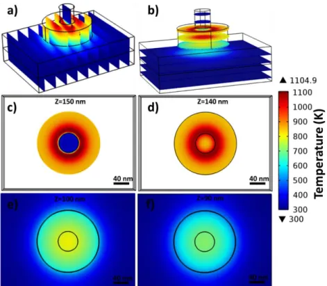
First, a voltage pulse of 1V pulse amplitude with 100 ns width and 42 ns trailing edge is applied to device in the simulation to understand temperature distribution inside the device for each layers during Set operation. Fig. 2 shows 3D temperature distribution inside device for
two different GST layers: first 80 nm diameter circular GST2 and a 350 nm square GST1 In Fig. 2, a color map of local temperature is given to illustrate heating profile inside device.
Fig. 2. A three dimensional illustration of temperature distribution is plotted for different vertical and horizontal slices for (a)–(b) and horizontal slices at different z values (c)-(f) for 25 nm circular top contact heater device. Simulations represent the temperature
distribution inside two GST layers during a programming voltage pulse of 1V, with 100ns width and 42ns trailing edge.
A 3D temperature illustration is plotted for different vertical and horizontal; vertical slices in (a)–(b) and horizontal slices at different z values (c)-(f) for 25 nm circular top contact device (heater). I specifically want to show the horizontal slice, 10 nm below the interface between the top contact heater and the GST2 layer (Fig. 2 c) – d)) and between the GST2 and the GST1 layer (Fig. 2 e) – f)). This is important to understand phase transition during switching and especially to see clearly the temperature differences for further phase transition.
The maximum temperature is obtained at the periphery of the top contact heater for GST2 (active region) with a homogeneous distribution. It is clearly visible in Fig. 2 for both GST layers, due to the top contact shapes for each of them, we have ho mogeneous temperature distribution, but this is just for temperature distribution, not for phase change distribution. (For more detail look for Cinar 2015)
3.2. Phase Distribution
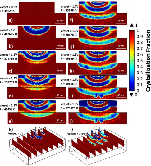
In all simulations, the system is initially all-crystalline state. After the application different magnitude of voltage pulses with a 100 ns width with a 42 ns trailing edge, the simulation results for phase transition are reported in Fig. 3 to compare the effects of homogeneous and heterogeneous current distributions through GST layers after Set operation. f the local crystallization fraction is shown for vertical cross sections of GST layers taken through the center Fig. 3 a)- j) and two vertical slice Fig. 3 k)- l) to justify the three dimensional phase distribution.
Fig. 3. Crystallization fraction, f, inside the PCM layers is shown for circular top contact PCM cells after the application of a 100 ns reset pulse with a 42 ns trailing edge. The color scale corresponds to f=1, red, for crystalline and f=0, blue, for amorphous phases. The
colors between the two represent regions with a mixture of crystalline and amorphous phases. A vertical cross-section of the device taken through the center is given for different pulse amplitudes resulting in different device resistances.
Figure 3a) shows clearly a crystalline state, which is low resistance state, and its resistance value is 3462 Ω after application of 0.9 C voltage pulse. However, when a reset pulse of 1V was applied to device, it was just enough for switching from crystalline to amorphous state for GST2 layer, high resistance state (not highest). Dome-shaped active region became amorphous and the device resistance is 482625 Ω, as in Fig. 3b). This voltage value is important, because 1 V pulse doesn’t cause any structural change in the GST1 as seen in Fig. 3b), but just enough to switch GST2 layer. It can be seen easily from the Fig. 2, this applied pulse is enough to heat around 600 K, 700 K or a little more but not enough for melting temperature of GST1.
Even though the GST1 layer was heated above Tm with higher voltage pulses, there is enough time for rearrangement of the atoms at high temperature, material goes to crystalline state again, because while GST2 layer was switching, GST1 layer stayed long time in high temperature. Therefore, for GST1 layer, mixed phases were obtained as it can be seen in Fig. 3c)-j).
There is an interesting phenomenon seeing in the device especially after 1.1 V voltage pulse, in the GST layer, a heterogeneous phase with both amorphous and crystalline phases as demonstrated by green to yellow colored regions is induced in Fig. 3 c)-j). The device resistance values are decreasing with increase in the voltage pulse from 462625 Ω to 10638 Ω values up to 1.7 V value as it can be seen in Fig. 3. Depending on the percentage of crystallization fraction f, the device resistance is changed. These states can be called as middle resistance states between low state and high state. For 1.8 V voltage pulse, the resistance of the device increased because of the switching in GST1 and also extensive increase amorphous region in GST2 layer. After this abrupt resistance increase, a resistance decrease with increase in programming voltage value was observed. However, at the beginning, the expected behavior is to observe one by one switching for each GST layers. Despite of the expectation, a lot of middle resistance states and fully switching for GST2 layer was observed and partially switched GST1 layer.
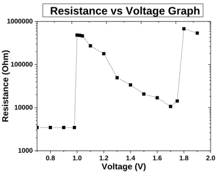
0.8 1.0 1.2 1.4 1.6 1.8 2.0 1000 10000 100000 1000000
Resistance (Ohm
)
Voltage (V)
Resistance vs Voltage Graph
Fig. 4. Simulation results of Set operation for increasing programming voltages for a 100 ns width pulse with 42 ns trailing edge. Applied voltage pulses and the resistance values obtained from the simulations are illustrated clearly in Fig. 4. Simulations show an abrupt switching in the 80 nm circular GST2 layer around 1V as seen in Fig. 4. Then a lot of middle resistance states with increase in voltage pulse amplitudes were observed. However, another abrupt switching in the resistance of the device was obtained at 1.8V. This is due to fully switching GST2 layer and partially switched GST1 layer. When the programming voltage value is increased, the resistance of the device decreases because GST1 layer turns into the crystalline state due to long time passing while GST2 layer is staying in high temperature even after voltage pulse. The reason behind of this is that the active layers are the same materials. And this gives enough time to GST1 layer for rearrangement of atoms in the heated regions to turn into the crystalline state.
4. Conclusions and Recommendations
In summary, for an optimum multiple bit per memory device. I have investigated the possibility of having stable middle resistance states in double active layers semiconductor device based on Ge2Sb2Te5/Ge2Sb2Te5 by using the high contrast between the crystalline and amorphous phases. To visualize the complex the nature of phase change dynamics, a comprehensive three dimensional finite-element model was developed by taking into account not only the electrical and thermal properties of the materials including thermoelectric effect, but also the homogeneous and heterogeneous nucleation and growth kinetics. By using this approach, the relation between the phase and electrical properties of device can be exhibited. This simulation results also show the importance of the selection of the materials. Therefore, beside the modification of the device shape, material selection is also another important factor to fabricate a semiconductor memory device with multiple bit per cell storage capability.
References
A. Cywar, J. Li, C. Lam, and H. Silva, The impact of heater-recess and load matching in phase change memory mushroom cells, Nanotechnology 23, 225201 (2012).
A. Pirovano, A. L. Lacaita, A. Benvenuti, F. Pellizzer, and R. Bez, Electronic switching in phase-change memories, IEEE Trans. Electron Devices 51, 452 (2004).
B. Liu, T. Zhang, J. Xia, Z. Song, S. Feng, and B. Chen, Nitrogen-implanted Ge2Sb2Te5 film used as multilevel storage media for phase change random access memory, Semicond. Sci. Technol. 19, L61 (2004).
C. Ip, Selenium inhibition of chemical carcinogenesis, Fed. Proc. 44, 2573–2578 (1984)
C. Peng, L. Cheng, and M. Mansuripur, Experimental and theoretical investigations of laser-induced crystallization and amorphization in phase-change optical recording media, J. Appl. Phys. 82, 4183 (1997).
D. A. G. Bruggeman, Berechnung verschiedener physikalischer Konstanten von heterogenen Substanzen. I. Dielektrizitätskonstanten und Leitfähigkeiten der Mischkörper aus isotropen Substanzen, Ann. Phys. 416, 636 (1935).
G. Bakan, A. Gokirmak, and H. Silva, Suppression of thermoelectric Thomson effect in silicon microwires under large electrical bias and implications for phase-change memory devices, J. Appl. Phys. 116, 234507 (2014)
G. W. Burr, M. J. Breitwisch, M. Franceschini, D. Garetto, K. Gopalakrishnan, B. Jackson, B. Kurdi, C. Lam, L. A. Lastras, A. Padilla, B. Rajendran, S. Raoux, and R. S. Shenoy, Phase change memory technology, J. Vac. Sci. Technol., B 28, 223 (2010). H.-S. P. Wong, S. Raoux, S. Kim, J. Liang, J. P. Reifenberg, B. Rajendran, M. Asheghi, and K. E. Goodson, Phase Change Memory,
Proc. IEEE 98, 2201 (2010).
I. Cinar, O. B. Aslan, A. Gokce, O. Dincer, V. Karakas, B. Stipe, J. A. Katine, G. Aktas, and O. Ozatay, Three dimensional finite element modeling and characterization of intermediate states in single active layer phase change memory devices, J. Appl. Phys. 117, 214302 (2015)
J. Lee, T. Kodama, Y. Won, M. Asheghi, and K. E. Goodson, Phase purity and the thermoelectric properties of Ge2Sb2Te5 films down to 25 nm thickness, J. Appl. Phys. 112, 014902 (2012).
J. Reifenberg, E. Pop, A. Gibby, S. Wong, and K. Goodson, Multiphysics modeling and impact of thermal boundary resistance in phase change memory devices, Proceedings of ITHERM (2006), pp. 106–113.
J. Tominaga et al., Ferroelectric catastrophe: beyond nanometer-scale optical resolution. Nanotechnology 15, 411–415 (2004)
K.-F. Kao, C.-M. Lee, M.-J. Chen, M.-J. Tsai, and T.-S. Chin, Ga2Te3Sb5—A Candidate for Fast and Ultralong Retention Phase‐Change Memory, Adv. Mater. 21, 1695 (2009).
L.C. Clark, G.F. Combs Jr., B.W. Turnbull et al., The nutritional prevention of cancer with selenium 1983–1993: a randomized clinical trial, J. Am. Med. Assoc. 276, 1957–1963 (1996)
M. Popescu, Non-crystalline solids, past, present, future. J. Non-Cryst. Solids 352(9–20), 887–891 (2006) M. Wuttig and N. Yamada, Phase-change materials for rewriteable data storage, Nat. Mater. 6, 824 (2007).
M. Yamaguchi, T. Togashi, S. Jinno, H. Kudo, E. Muramatsu, S. Taniguchi, A. Inoue, 4.7 GB phase-change optical disc with in-groove recording, Jpn. J. Appl. Phys. 1 38(3B), 1806–1810, (1999)
M.H. Brodsky, Amorphous Semiconductors (Springer Verlag, New York, 1985),
N. Yamada, E. Ohno, K. Nishiuchi, N. Akahira, and M. Takao, Rapid‐phase transitions of GeTe‐Sb2Te3 pseudobinary amorphous thin films for an optical disk memory, J. Appl. Phys. 69, 2849 (1991).
O. Ozatay, B. Stipe, J. A. Katine, and B. D. Terris, Electrical switching dynamics in circular and rectangular Ge2Sb2Te5 nanopillar phase change memory devices, J. Appl. Phys. 104, 084507 (2008).
P. Fiflis, L. Kirsch, D. Andruczyk, D. Curreli, and D. N. Ruzic, Seebeck coefficient measurements on Li, Sn, Ta, Mo, and W, J. Nucl. Mater. 438, 224 (2013).
S. Raoux, G. W. Burr, M. J. Breitwisch, C. T. Rettner, Y.-C. Chen, R. M. Shelby, M. Salinga, D. Krebs, S.-H. Chen, and H.-L. Lung, Phase-change random access memory: A scalable technology, IBM J. Res. Dev. 52, 465 (2008).
S. Raoux, W. Wełnic, and D. Ielmini, Phase change materials and their application to nonvolatile memories. Chem. Rev. 110, 240 (2010).
S.-H. Hong, H. Lee, K.-I. Kim, Y. Choi, and Y.-K. Lee, Fabrication of Multilevel Switching High Density Phase Change Data Recording Using Stacked GeTe/GeSbTe Structure, Jpn. J. Appl. Phys., Part 1 50, 081201 (2011).
S.-H. Hong, H. Lee, Y. Choi, and Y.-K. Lee, abrication of multi-level switching phase change nano-pillar device using InSe/GeSbTe stacked structure, Curr. Appl. Phys. 11, S16 (2011).
T.E. Schlesinger, J.E. Toney, H. Yoon, E.Y. Lee, B.A. Brunett, L. Franks, R.B. James, Cadmium zinc telluride and its use as a nuclear radiation detector material, Mater. Sci. Eng. 32, 103 (2001)
W. Welnic and M. Wuttig, Reversible switching in phase-change materials, Mater. Today 11, 20 (2008).
XU Cheng, LIU Bo, CHEN Yi-Feng, LIANG Shuang, SONG Zhi-Tang, FENG Song-Lin, WAN Xu-Dong, YANG Zuo-Ya, XIE Joseph, CHEN Bomy, Switching Characteristics of Phase Change Memory Cell Integrated with Metal-Oxide Semiconductor Field Effect Transistor, Chin. Phys. Lett. 25, 1848 (2008).
Y. Gu, Z. Song, T. Zhang, B. Liu, and S. Feng, Novel phase-change material GeSbSe for application of three-level phase-change random access memory, Solid-State Electron. 54, 443 (2010).
Y. N. Hwang, J. S. Hong, and S. H. Lee, et al, Phase-change chalcogenide nonvolatile RAM completely based on CMOS technology, Symp. VLSI Technol., Dig. Tech. Pap. 29–31 (2003).
Y. Won, J. Lee, M. Asheghi, T. W. Kenny, et al, Phase and thickness dependent modulus of Ge2Sb2Te5 films down to 25 nm thickness, Appl. Phys. Lett. 100, 161905 (2012).