Contents lists available atScienceDirect
Results in Physics
journal homepage:www.elsevier.com/locate/rinp
The physical properties of bismuth replacement in lead halogen perovskite
solar cells: CH
3
NH
3
Pb
1−x
Bi
x
I
3
compounds by ab-initio calculations
C. Soykan
a,⁎, H. Gocmez
baVocational School of Health Services, Ahi Evran University, Kırşehir, Turkey
bDepartment of Metallurgy and Materials Engineering, Dumlupınar University, Kütahya, Turkey
A B S T R A C T
The selection of elements used in the design of solar cells is crucial in terms of environmental pollution and legalization problems due to the fact that both solar energy conversion efficiency as high as possible and toxic effects when dissolved in water. Hybrid Pb halogen solar cells demonstrate promising solar cell conversion material properties with a conversion rate of approximately 20%. However, Pb is a toxic element when dissolved in water. In this study, it was aimed to design new material forms for solar cells obtained by replacing Pb with a less toxic element without disrupting the photophysical properties of the material. This approach has been exemplified by focusing on bismuth considering Goldschmidt rules (GRs), Tolerance factor concept (t) and Shockley Queisser (SQ) limits. Non-stoichiometric CH3NH3Pb(1−x)Bi(x)I3crystal structure were formed at the ratios determined by x = 0.125, 0.25, 0.75 and 1.00 values by replacingBi3+withPb2+. Using the Density Functional Theory (DFT), the effect of added Bismuth ions in the structural and electronic properties of the material was investigated. According to the Shockley Quisser (SQ) limit, the crystal form CH3NH3Pb0.875Bi0.125I3formed with x = 0.125 ratio was determined to be the most suitable structure in terms of solar cell productivity with a direct band gap of 1.30 eV. In addition, the band gaps of CH3NH3Pb0.500Bi0.500I3and CH3NH3Pb0.250Bi0.750I3formed at x = 0.50 and 0.75 were calculated to be 1.0863 eV and 1.0895 eV, respectively. Band gaps of these phases were also within the SQ limit. However, the band gap of the CH3NH3PbI3 stoichiometric phase was calculated to be 1.6826 eV above the SQ limit, while the CH3NH3BiI3phase band gap was calculated to be 0.2738 eV well below the SQ limit. According to our DFT calculations, organic halogen perovskite compounds in the form of CH3NH3Pb(1−x)Bi(x)I3formed at ratios of x = 0.125, 0.50 and 0.75 have been found to be more efficient than CH3NH3PbI3compounds in terms of solar energy conversion capacity, optoelectronic systems and environmental safety.
Introduction
Inorganic and organic hybrid perovskite solar cells are notable for their high power conversion efficiencies and low production costs. It has being studied to improve the electronic and optical properties of such solar cells. The dependence of theCH NH PbX+
3 3 3 (X=CI Br I, , )
crystal structure on the temperature was investigated by Poglitsch and Weber with x-ray diffraction[1]. TheCH NH PbI+
3 3 3 structure was found
to have a tetragonal crystal structure with space group I4/m or I4/mcm at room temperature and a cubic phase transformation was observed at Tc= 327.4 K[1]. It was found a phase transformation from the
tetra-gonal to orthorhombic symmetry (space group Pna21), which shows that a central symmetric unit cell passes through a central non-sym-metric unit cell [1]. This transition can cause the material to have ferroelectric and antiferroelectric properties. Thus, it is likely that the electronic properties of the material, such as the band gap, will change. The electronic and optical properties of CH3NH3PbI3, CH3NH3PbI3BF4, CH3NH3PbI(BF4)2 and CH3NH3PbI(BF4)2 perovskite phases were in-vestigated using the first principles method by Rani and Singh based on Density Functional Theory (DFT)[2]. In the study of Rani, the band gap of CH3NH3PbI3 crystal form are calculated as 1.73 eV. The
configuration for solar cell of the perovskite CH3NH3Pb1−xSbxI3(x = 0 ve 0.15) crystal structure by using Rietveld treatment technique are studied by Ando and et al.[3]. When Ando's results are examined, the addition of Sb atoms with a smaller atomic radius instead of Pb atoms reduces the lattice constant of the material. This effect also results in the expansion of the band gap. Mosconi et al.[4]have been indicated that organometal CH3NH3PbX3 and mixed halide CH3NH3PbI2X (X = CI, Br, I) perovskite materials are important for highly productive solid-state cells. It is also stated that the interaction of the organic and inorganic components mediated by the hydrogen bond between the ammonium and halide groups in the work plays an important role on the structural variability of the material [4]. Kojima et al. [5]have focused on the Pb halide perovskite CH3NH3PbBr3 and CH3NH3PbI3 compounds for visible light sensitizing functions in photoelec-trochemical cells. They reported that CH3NH3PbI3 based cells can convert solar energy to 3.8% efficiency and a high photovoltage yield of 0.96 V. Saffari et al.[6] have investigated the structural and optical properties of chlorine doped non-stoichiometric CH3NH3PbI3−xCIx
(x = 0, 1, 2, 3) perovskite cubic phase by using DFT method. By using the data obtained here, they have studied properties such as light ab-sorption efficiency and single-juk optical current density. The results
https://doi.org/10.1016/j.rinp.2019.102278
Received 24 January 2019; Received in revised form 2 April 2019; Accepted 6 April 2019 ⁎Corresponding author.
E-mail address:[email protected](C. Soykan).
Available online 13 April 2019
2211-3797/ © 2019 The Authors. Published by Elsevier B.V. This is an open access article under the CC BY-NC-ND license (http://creativecommons.org/licenses/BY-NC-ND/4.0/).
show that when chlorine is doped, the band gap increases; the lattice constants, the optical properties such as reactive index and damping coefficient decrease. Although organic Pb halogen perovskite com-pounds are an important material in terms of conversion efficiency of solar energy, a solar cell technology based on water-soluble Pb seems to be disadvantages due to environmental pollution and legalization pro-blems. For this reason, it is important to investigate materials with good photoelectric properties by using less toxic elements instead of Pb. Ja-cobsson et al.[7]have investigated other metal ions that could be re-placed in place of Pb, adhering to the Goldschmidt (GRs) rules and also taking into account the quantum mechanics . Sr2+ ion, whose ionic radius is almost the same as Pb2+, was used. Strontium is a relatively inexpensive and non-toxic element. However, the band gap of CH3NH3SrI3was calculated to be 3.6 eV, which was too high for effi-cient photo-absorption. This study only revealed CH3NH3SrI3 per-ovskite crystal structure[7]. Recently, it has worked on modeling Bis-muth addition to CH3NH3PbI3perovskite structure using first-principle methods by Mosconi and et al. [8]. It has been reported that hetero-valent Bi doping to the perovskite structures was limited in terms of efficiency and the doped Bi3+ions acted as a deep electron trap. The details of the Goldschmidt empirical replacement rules (GRs) used in studies based on the element displacement approach are also given in Goldschmidt's study on the laws of crystal chemistry[9].
There are some physical limits in the crystal structures when the photoelectric converter solar cells are produced. First, the use of toxic elements in water-soluble cells causes environmental pollution and le-galization problems. Second, although the doping of non-toxic elements instead of Pb seems to be a solution, limitations such as the Shockley Queisser limit and the Goldschmidt tolerance factor determine the number of elements that can be used. In addition, the value of the band gap of the material to be used for the ideal conversion efficiency is also very important. CH3NH3PbI3 perovskite crystal form consists of
+
CH NH3 3 organic group (A cation),Pb2+cation (B cation) and halogen
I anion (C anion). The crystal ionic radius ofCH NH+
3 3 organic cation is
0.180 nm, forPb2+it is 0.132 nm and forI it is 0.206 nm[10]. The crystal ionic radius of Bi3+ is given as 0.117 nm[11]. In this study, according to x = 0.125, 0.25, 0.50, 0.75 and 1.00 ratios, non-stoi-chiometric CH3NH3Pb(1−x)Bi(x)I3forms are constructed by dopingBi3+ instead ofPb2+. Using the Goldschmidt rules, Shockley Queisser limit, quantum mechanical approach and DFT calculation techniques, it is aimed to investigate photophysics of metal halogen perovskites and to determine the structural and electronic properties of the new hybrid solar cells by examining the contribution of promisingBi3+instead of
+
Pb2 . In addition, to the best of our knowledge, no detailed theoretical
or experimental data concerning non-stoichiometric CH3NH3Pb(1−x)Bi(x)I3perovskites for x values from 0.125 to 1.00 have been reported in the literature.
Computational method
In this study, ab-initio simulation calculations based on the Density Functional Theory (DFT) were performed using the potential of the projector augmented wave (PAW) to solve the Kohn-Sham equations [12–14]. Total energy calculations were performed using the Vienna ab-initio simulation package (VASP)[15–19]. The effects of electronic exchange and correlation functions were considered using the Gen-eralized Gradient Approximation (GGA) developed by Burke, Perdew and Ernzerhof[20]. In our calculations, kinetic energy cutoff value for CH3NH3PbI3crystal phase was determined to be 600 eV. The energy convergence criterion of the electronic self-consistency was chosen as 10−8eV/atom [21]. In the non-stoichiometric CH
3NH3Pb(1−x)Bi(x)I3 phases, a kinetic energy cut-off value of 500 eV and convergence value 10−8eV/atom were used. The Brillouin zone integrations were carried out by Monkhorst-Pack special points mesh with a grid size of 12x12x12 (for CH3NH3PbI3and CH3NH3BiI3) and 6x6x6 (for marten-sitic CH3NH3Pb(1−x)Bi(x)I3)[22]. The contribution of valence electrons
is influential in determining the electronic properties of material. The valence electron configurations for C, N, H, Pb, Bi and I atoms are 2 s2 2p2, 2 s22p3, 1 s1, 5d106 s26p2, 5d106 s26p3and 5 s25p5, respectively. Generally known, geometric optimization calculations have been made to determine the equilibrium state with the smallest energy. To de-termine the electronic behavior of the material, the density of states (DOS) was calculated using the tetrahedron method involving Bloch corrections. In addition, partial density of states (pDOS) calculations have been carried out to examine in more detail the contributions of the Pb, Bi and I atoms to the electron density of the material. The cubic CH3NH3PbI3crystal lattice was iterated by 2x2x2 ratio and transformed into super-lattice.Bi3+ions instead ofPb2+ions were placed according to x values to form non-stoichiometric CH3NH3Pb(1−x)Bi(x)I3 crystal phases. As a result of Sr, CI, Br, Co, Ca and Bi substitutions to the perovskite crystal structure, studies have been focused on the changes in the physical properties of the structures. On the other hand, among these atoms, it was particularly focused on the dopant of Bi3+ ion [23–28]. Besides, The difference between the ionic radius of Bi3+and the ionic radius of Pb2+is about 11.36%. Since this value is less than 15%, it can be said that a full compliance can be achieved in terms of Goldschmidt's empirical substitution rules. In addition, the Bi3+and Pb2+cations are isoelectronic (6 s2) and have similar chemical prop-erties[11]. Bi3+has a stable oxidation state of + 3. Since it has similar ionic radius and electronic structure with Pb2+, it can be expected to be similar in optoelectronic properties[29]. Since the Bi3+ion has a si-milar ionic radius as Pb2+, it is expected to substitute the position of the Pb2+ions in the perovskite crystal structure. However, Mosconi et al. [8]reported that the doped Bi3+ions behavior as a deep electron trap. On the other hand, it has been shown by Snaith et al.[28]that the color change seen in the Bi-doped CH3NH3PbI3 crystal occurs due to in-creased defect states and to increase in the sub-band gap density of states.
In our calculations, there are 12 atoms in CH3NH3PbI3crystal phase and 50 valence electrons (read from the POTCAR file) in total. Similarly, in the CH3NH3BiI3phase there are also 12 atoms and 51 valence electrons (read from the POTCAR file). The same approach was also used in the calculation of non-stoichiometric crystal structures. At the beginning of our stoichiometric and non-stoichiometric calculations for heterovalent doping, we used the “nelect” parameter to consider the change in the total number of valence electrons of the crystal structures due to the addition of Bi3+ion. It should not be forgotten that, as is known, with the vasp code only the total number of valence electrons of the system can be controlled. In addition, the vasp code will auto-matically add a background jellium to make the supercell in neutral charge and the jellium charge is distributed in the volume[15–19]. The calculations were first initiated from the cubic CH3NH3PbI3 crystal phase, which had a stoichiometric 12 atom (containing C 1, N 1, H 6, Pb 1 and I 3 atoms). Space group of cubic crystal structure of CH3NH3PbI3 is space group 221 (Pm m Pm m3 , 3 orIm m3 ). The position of atoms in crystal structure is given by C (0.896, 0.999, 0988), N (0.142, 0.999, 0,032), H (0.866, 0.999, 0.805; 0.822, 0.152, 0.064; 0.822, 0.847, 0.065; 0.221, 0.142, 0.965; 0.221, 0.856,0.965; 0.180, 0.999, 0.205), Pb (0.475, 0.500, 0.477) and I (0.428, 0.499, 0.972; 0.433, 0.000, 0.512; 0.967, 0.500, 0.439), respectively. After the crystal lattice was relaxed, the electronic density of state (DOS) and partial density of state (pDOS) were calculated. Stoichiometric unit cells containing 1 Pb and 1Bi atoms are given inFig. 1. In the second step, the relaxation and electronic state densities (DOS and pDOS) of the non-stoichiometric CH3NH3Pb(1−x)Bi(x)I3structure were calculated. Super-lattice of non-stoichiometric crystal structures are given also inFig. 2a)–d), respec-tively. Crystal structure of nonstoichiometric phases were obtained by using initial cubic structure of CH3NH3PbI3 that is created with ex-tension by 2x2x2 through ×, y and z directions. After Bi atoms were positioned at proper location in the structure, the obtained new phase was relaxed until the defined conditions were reached. This calculation
reveals that final relaxed and stable crystals phase has orthorhombic structure with space group 33 (Pna21)
The concept of tolerance factor (t) for perovskite structures should be considered in order to examine process of the placement ofBi3+ion instead ofPb2+cation at x = 0.125, 0.25, 0.50, 0.75 ratios in organic halogen perovskite material in terms of Goldschmidt's rules. The tol-erance factor, t, with respect to the ionic radius of the actual ions is given as follows: = + + t r r r r 2 ( ) A C B C (1)
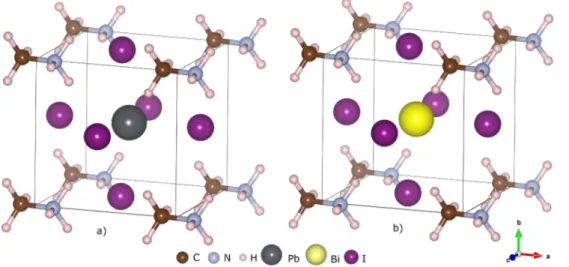
where rA,rB verC are the ionic radius of the A, B and C ions,re-spectively. It has been reported that; If the value of the tolerance factor t is 0.7 < t less than 0.9, the crystal structure is tetragonal, orthor-hombic or rhombohedral (the A cation can be too small or the B cation can be very large); If 0.9 < t less than 1.0, the crystal structure can be cubic crystal phase (ideal perovskite crystal structure); if t > 1.0; the Fig. 1. a) CH3NH3PbI3and b) CH3NH3BiI3 perovskite cubic and orthorhombic phases unit cell crystal structures. Brown, gray, cream, black, yellow and purple circles in the pictures represent C, N, H, Pb, Bi and I atoms, respectively. (For interpretation of the references to color in this figure legend, the reader is referred to the web version of this article.)
Fig. 2. The super cell crystal structures of CH3NH3Pb(1−x)BixI3perovskite phases are designed by x ratio a) 0.125, b) 0.25, c) 0.50 and d) 0.75, respectively. Brown, gray, cream, black, yellow and purple circles in the pictures represent C, N, H, Pb, Bi and I atoms, respectively. (For interpretation of the references to color in this figure legend, the reader is referred to the web version of this article.)
crystal structure be multi-layered crystal phases (A cation can be too large) [30,31,32]. According to Eq. (1), the tolerance factor (t) was calculated to be 0.85 for the crystal structure acquired from the addi-tion ofBi3+ion in place of thePb2+. The 0.85 value indicates that the perovskite is not cubic at room temperature, while obtained crystal structure is very close to the ideal perovskite cubic boundary. The empirical rules for element substitution with respect to Goldschmidt, if the ionic radius differs by less than 15%, a full perfectly substitution can occur, but, if the size differs between 15 and 30%, limited substitution can occur. Thus, the charge of the material changes and the charge neutrality is restored by changing the charges of the other elements[9]. The difference between the ionic radius (0.117 nm) ofBi3+and the ionic radius (0.132 nm) of Pb2+ is approximately 11.36%. This difference, according to Goldshmidt's empirical substitution rules, is less than 15%, indicating that substitution can easily occur. As a result of our calcu-lations, as given in Tables 1 and 2, the stoichiometric and non-stoi-chiometric perovskite structures are transformed to the orthorhombic crystal form when by added Bi3+ ions with respect to x ratio. The transition of stable crystal phases to orthorhombic symmetry corre-sponding to the minimum energy reached as a result of the simulation is a consequence of methylammonium cations not having a spherical symmetry.
Results and discussion
Structural properties of stoichiometric phases
CH3NH3PbI3 perovskite material has been reported by previous theoretical[4,7,33]and experimental[3,34,35] studies in which the cubic (Pm3m), tetragonal (I4/mcm) and orthorhombic (Pna21) crystal phases were defined. In this study, the structural and electronic prop-erties of the CH3NH3PbI3crystal form were calculated. There are 1C, 1 N, 6H, 1 Pb and 3 I atoms in CH3NH3PbI3given inFig. 1a) unit cell with 12 atom. As given inFig. 1b) the CH3NH3BiI3crystal form with 12 atoms are obtained by doping Bi3+ions instead of Pb2+ions.
In our calculations, the lattice constant of the cubic phase of CH3NH3PbI3 was calculated as 6.406A0 with a unit cell volume of
A
262.88 3. The calculated lattice constant is consistent with the
theoretical data in the range of from6.172A0to6.420A0[2,4,6,33]and
also the experimental lattice constants varying between 6.180A0and
A
6.288 0[1,3,34]. The lattice constant calculated as6.406A0differs 2–3%
ratio deviation from the experimental data. The lattice constants of CH3NH3BiI3phase are also calculated as6.967 , 6.064A0 A0 and6.155A0. The lattice constants of the CH3NH3BiI3crystal formed by the addition of 1 mol of Bi3+ion instead of 1 mol of Pb2 + were estimated to be about 9%, 5% and 4% deviation ratio from the cubic phase, respec-tively. Our results are presented inTable 1for comparison with other experimental and theoretical studies.
Structural properties of Non-stoichiometric phases
The crystal structure of CH3NH3PbI3given inFig. 1a) was selected as the initial phase and x = 0.125 was taken to form the first non-stoichiometric CH3NH3Pb(1−x)Bi(x)I3structure. The crystal lattice was shifted to 2x2x2 (containing C 8, N 8, H 48, Pb 7, Bi 1 and I 24 atoms) have been obtained the CH3NH3Pb0.75Bi0.25I3supercell. This supercell is given inFig. 2a).
Similarly, x = 0.25, 0.50 and 0.75 were selected to obtain CH3NH3Pb0.750Bi0.250I3, CH3NH3Pb0.500Bi0.500I3 and CH3NH3 -Pb0.250Bi0.750I3, respectively. Supercells of these phases are presented in Fig. 2b)–d), respectively.
In the geometric optimization calculations, the structural properties of the crystal phases in the equilibrium state are calculated when the external pressure applied to the crystal is about 0 kbar and the total force applied on each atom reaches about0.01eV A/ 0. The results
ob-tained are listed inTable 2.
Based on the varying x values from 0.125 to 0.75, it was determined that the additionBi3+ions instead ofPb2+ions did not alter the crystal lattice constants and the angles between the ×, y, and z directions. However, the lattice constants calculated for the non-stoichiometric CH3NH3Pb(1−x)BixI3 phases deviate 0.6%, 0.008% and 1.38% ratios, respectively, from the lattice constant of the initial phase CH3NH3PbI3 (6.406A0). It is seen that the crystal structures of the non-stoichiometric
phases are transformed from the cubic phase to orthorhombic phase, while the deviation rates in the lattice constants are very small. This result supports the crystal form (orthorhombic) predicted by the value of the tolerance factor calculated as 0.85 for the addedBi3+ions crystal phase depending on the x values.
Electronic properties of stoichiometric phases
The total electron state density (DOS) of the stoichiometric CH3NH3PbI3 and CH3NH3BiI3 phases and the partial (pDOS), which describes the contributions from the individual electronic states, are shown inFig. 3a) and b), respectively. The Fermi level is shifted to 0 eV in the all figures. When examining the electronic properties of the CH3NH3PbI3 structure given in Fig. 3a), the lowest valence bands around −8 eV are predominantly due to the states 6 s-6p and 5d of the Pb atoms. The valence band between −3 eV and the Fermi level pre-dominantly consists of the 5 s and 5p states of the I atoms. In the conduction band distributed between 2 eV and 6 eV, especially the states s, p and d of the Pb atoms dominate in the contributions coming Table 1
The lattice constants of the stoichiometric CH3NH3PbI3and CH3NH3BiI3crystal structures and the other theoretical and experimental data.
Structure Method Lattice Constants (A0) Ref.
a b c
CH3NH3PbI3 our cal. 6.406 6.406 6.406
other cal. 6.420 6.420 6.420 [2] 6.330 6.330 6.330 [4] 6.310 6.310 6.320 [6] 6.172 6.149 6.218 [33] exp. 6.328 6.328 6.328 [1] 6.288 6.288 6.288 [3] 6.180 6.180 6.180 [34]
CH3NH3BiI3 our cal. 6.967 6.064 6.155
Table 2
The calculated lattice constants of non-stoichiometric crystal structures of CH3NH3Pb(1−x)BixI3perovskite phases are designed by x ratio a) 0.125, b) 0.25, c) 0.50 and d) 0.75, respectively.
Structure x ratio Lattice constants (A0) Angles between ×, y, and z directions
a b c
CH3NH3Pb0.875Bi0.125I3 0.125 6.443 6.406 6.494 90.024 89.841 90.019
CH3NH3Pb0.750Bi0.250I3 0.250 6.443 6.406 6.494 90.024 89.841 90.019
CH3NH3Pb0.500Bi0.500I3 0.500 6.443 6.406 6.494 90.024 89.841 90.019
to the lower parts of the band. In the 3 eV and higher parts, contribu-tions of both Pb and I atoms have been observed. The top part of the valence band is at −0.246 eV and the bottom part of the conduction band is at 1.4362 eV. In the R symmetry point, the presence of both the top part of the valence band and the bottom part of the conduction
band indicates that the cubic CH3NH3PbI3phase has an electronic di-rect band gap. The band gap are calculated as 1.6826 eV. The obtained results are given in Table 3for comparison with other studies. The calculated band gap in this study is compatible with both theoretical and experimental studies. However, it shows a deviation of at least 3% Fig. 3. The calculated band structures of the stoichiometric a) CH3NH3PbI3and b) CH3NH3BiI3phases in the direction F R M F. In order to increase the resolution, the R Mline is zoomed. The fermi level is at 0 eV.
and at most 11% from the theoretical studies. In terms of experimental studies, it was very consistent with the value given in[36], but deviated by 8% from other studies.
Fig. 3b) shows the electronic band distribution of the CH3NH3BiI3 phase. In both the valence-conduction bands and the high-low energy regions, the contributions in the 6 s- 6p and 5d states of the Bi atoms are rather dominant over the contributions from the other atoms. However, the highest level of the valence band is at the R symmetry point of −0.128 eV, while the lowest level of the conduction band is at the M symmetry point of 0.1451 eV. Thus, the energy band gap of the CH3NH3BiI3phase was calculated to be a very small value of 0.2738 eV. Due to the top point of the valence band and the bottom point of the conduction band are located at different symmetry points (R and M), it is seen that the CH3NH3BiI3phase has an electronic indirect band gap. WhenFig. 3a) and b) are examined, while the peak of the valence band maintains a value of −0.128 eV, the lowest level of the conduction band decreases from 1.4362 eV to 0.1451 eV. As a result of this change, a narrower band gap is formed. For the perovskite structures in the A B C3general form, the electronegativity of the B cation was
re-ported to be more effective on the band width than the A cation [39,40]. Accordingly, reducing the electronegativity of B cation will increase the band gap of the material. In addition, the character of the B C bond is also effective on band width and the increase in the antibonding character of the B C bond will also result in an increase in band gap[39]. Differences in orbit symmetries are a source of these effects and can lead to the possibility of different hybridizations. The electronegativity of Bi, Pb and I elements are given as 2.02, 2.33 and 2.66, respectively. Bismuth's electronegativity is relatively smaller than the electronegativity of lead. This would increase the antibonding character of the Bi I bonds by some amount relative to the Pb I bonds. While it was expected that the increase of the antibonding effect between the anion and the cation would increase the band gap, In our calculations, it was determined that the band gap by displacement of theBi3+ions is decreased due to approach of the conduction band to the valence band. In order to be able to explain this effect, it is necessary to focus on two physical properties. First, the difference between elec-tronegativity of Bi, Pb and I elements is rather small. This little differ-ence in electronegativity ensures that the change of antibonding char-acter is very small between Bi-I and Pb-I cation and anion bonds. Second, as explained by theoretical methods in Walsh's paper, the substitution of a cation with a smaller ionic radius reduces the band gap [41]. When this point of view, the ionic radius of the Pb element is 0.132 nm, while the ionic radius of the Bi element is 0.117 nm. Thus, the use of a smaller cation (Bi instead of Pb) will reduce the band gap of the crystal phase. Our work has shown that the effect of the reduction of the cation size on the band gap is more dominant than the influence of the change in the antibonding character of the bonds. As a result of this
effect, the band gap of the CH3NH3BiI3material is considerably reduced when compared to CH3NH3PbI3. However, the calculated band gap of 0.2738 eV is not the ideal band gap for a photoabsorber. The band gap of the CH3NH3BiI3crystal form is very poor in terms of usability in solar cells. Furthermore, the band gaps of the non-stoichiometric crystal forms described in the following sections yield promising results. Electronic properties of Non-stoichiometric phases
While investigating the electronic properties of the non-stoichio-metric CH3NH3Pb(1−x)BixI3material produced by varying x values from 0.125 to 0.750, the CH3NH3Pb0.875Bi0.125I3crystal structure of were first obtained by with x = 0.125. The super cell of this phase is given in Fig. 2a). The electron band distribution of the optimized crystal phase is calculated in the direction of F R M F. In order to increase the resolution, theR M symmetry points within the band gap region are zoomed. The electronic band distribution is given inFig. 4a). The band gap is calculated as 1.3057 eV. While the band gap of the stoichiometric CH3NH3PbI3structure is on the R symmetry point; in the non-stoichiometric CH3NH3Pb(1−x)BixI3forms, the band gap is observed at the symmetry point. As given inFig. 4a), electronic states under the valence band consist of contributions from Pb atoms in the range of −10 eV to −8 eV. while there is a small contribution from the s, p and d states of Pb atoms in the valence band between −4 eV and 0 eV, especially there are a contribution of the 5 s, 5p states of both I atoms in the valence band between −2 eV and −4 eV, which is not dominant of the contributions of the s, p and d states of both Pb and Bi atoms. Furthermore, the 5 s-p states of the I atoms contributes sig-nificantly to the overall distribution of the valence band. The effect of this contribution increases towards the top of valence band. In the conduction bands, while the contributions of Bi atoms is less in the bottom of conduction band, the effect of the Pb atoms increases towards high energy level as relatively (between 1 eV and 2 eV). In addition, the contribution of I atoms is dominant in the level between 1 eV and 4 eV. It has been determined that the addition of Bi3+ions instead of Pb2+ ions at x = 0.125 ratio to the supercell of the crystal reduces band gap by 22.4%. InFig. 4b) shows the electronic band and pDOS distribution of the CH3NH3Pb0.750Bi0.250I3crystal form. When the electronic band structure of the phase is examined, it is seen that the contributions from the individual atoms exhibit a similar behavior locally to the crystal structure of CH3NH3Pb0.875Bi0.125I3(x = 0.125). However, especially a distribution of the 6p states of Bi atoms significantly lowers the bottom level of the conduction band. Accordingly, the band gap of the CH3NH3Pb0.750Bi0.250I3 crystal structure was calculated to be 0.9254 eV. It has been determined that the CH3NH3Pb0.750Bi0.250I3 crystal phase obtained at x = 0.250 reduced the band gap value re-lative to the initial phase by 45%. The calculated band gap values are given inTable 4.
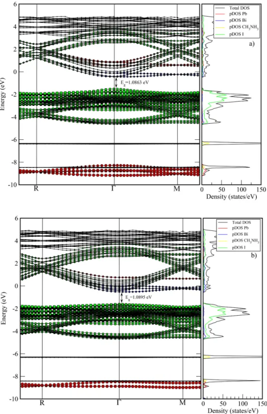
The electronic band and pDOS distribution of the CH3NH3Pb0.500Bi0.500I3and CH3NH3Pb0.250Bi0.750I3crystal phases are given inFig. 5a) and b), respectively. The band distribution in the two phases exhibits a similar electronic behavior. While the valence band predominantly contains contributions from the I atoms; it is seen in Fig. 5a) and b) that the contributions from the Bi atoms to the lower parts of the conduction band and from the Pb atoms to the middle parts and from the I atoms to the upper part are more visible. The electronic band gaps of both non-stoichiometric phases were calculated to be 1.0863 eV and 1.0895 eV, respectively. The electronic band gap of the phases CH3NH3Pb0.500Bi0.500I3and CH3NH3Pb0.250Bi0.750I3relative to the initial phase was calculated to be about 35% smaller. The combi-nation ofBi+3andPb+2 ions with respect to x ratios in the
non-stoi-chiometric crystal forms provides a mixed contribution of both the antibonding characteristic of Pb-I or Bi-I bonds and the effect of cation size on band gap. As a result of the common contribution of these two effects, the band gap is reduced, but at the efficiency limits it remains at the level of convenience. According to the Shockley Queisser (SQ) limit, Table 3
The calculated band gaps of the stoichiometric CH3NH3PbI3and CH3NH3BiI3 crystal structures and the other theoretical and experimental data.
Structure Method Band gap Ref.
Eband gap(eV)
CH3NH3PbI3 our cal. 1.682
other cal. 1.730 [2] 1.570 [4] 1.500 [6] 1.600 [7] 1.530 [8] 1.810 [33] exp. 1.550 [5] 1.550 [35] 1.610–1.680 [36] 1.600 [37] 1.550 [38]
the optimum range for the material to be used is 1.35 eV so that the best efficiency can be obtained from the solar cells [42]. A yield of ap-proximately 33% can be obtained for these band gap values. For this reason, it is important that for effectivity the material have a band gap of around 1–1.5 eV. When we evaluate our results according to the SQ limit, while the CH3NH3PbI3stoichiometric phase remains above the limit with 1.6826 eV band gap, the CH3NH3BiI3phase also remains well below the limit with 0.2738 eV band gap. In the non-stoichiometric
phases, it was calculated that the CH3NH3Pb0.875Bi0.125I3 crystal structure was the best band gap value. Although the band gaps of the CH3NH3Pb0.500Bi0.500I3and CH3NH3Pb0.250Bi0.750I3phases are within the limits of the SQ, the band gap of the CH3NH3Pb0.750Bi0.250I3phase was found to be below the limit of 1–1.5 eV.
As known, in semiconductor materials, both energy saving and crystal momentum should be maintained in order to ensure the passage of electron through the valence band to the conduction band. The Fig. 4. The calculated band structures of the non-stoichiometric CH3NH3Pb(1−x)BixI3phases designed with ratios a) x = 0.125 and b) x = 0.25 in the direction
maximum energy state in the valance band and the minimum energy state in the conduction band are each characterized by a certain crystal momentum (k-vector) in the Brillouin zone. If the k-vectors are the same, it is called a direct gap. If they are different, it is called an indirect gap. In cases where there is a direct band transition, the crystal mo-mentum is preserved. In addition, the photons have a very small crystal momentum. Therefore, the values can be taken as zero. The phonons have a higher crystal momentum than photons, although their energy is low. Accordingly, electron transition can be achieved by photon in materials with direct band gap. In materials with indirect band gap, for electron transition, there is a need for a phonon, which the crystal momentum of the phonon equal to the difference between the valence band maximum and the conduction band minimum. That is, while al-most all energy in the indirect band transition comes from the photon; all momentum comes from the phonon. In such transitions, since the electrons pass through the intermediate phases, they increase the crystal temperature because they transfer their energies to the crystal lattice. Therefore, the use of material with indirect band gap in op-toelectronic devices is unsuitable for efficiency. In opop-toelectronic de-vices and sun cells, direct band gap materials with higher optical ab-sorption coefficients and band transition supplied with photon energy should be preferred.***
In the CH3NH3BiI3stoichiometric crystal phase given inFig. 3b), the contribution from the atoms of Bi at both the Fermi level and the deeper parts of the conduction and valence band is significantly higher than the Pb, CH3NH3and I atoms. As mentioned in the study of Mosconi et al.,[8]Bi3+states behave like deep electron trap in Bi-doped per-ovskite structures. In this respect, while the electronic band gap of the CH3NH3PbI3crystal phase was calculated as 1.6826 eV, the electronic band gap of the CH3NH3BiI3phase obtained as a result of the Bi-doping was calculated as 0.2738 eV. We consider that this decrease in the band range is due to the increase in the potential electron traps of the ma-terial as a result of the Bi doping. However, an indirect electronic band transition in the R M direction for the CH3NH3BiI3phase was cal-culated. In terms of the efficiency of solar cells, CH3NH3BiI3 crystal form is not a good material candidate with indirect band transition of 0.2738 eV. In addition, it will not be efficient in terms of its use in optoelectronic devices since it has an indirect band transition. In terms of productivity, perovskite crystal structures show a limited capacity of Bi doping. As given in Fig. 4a), in the CH3NH3Pb0.875Bi0.125I3 phase formed by x = 0.125, there are very small contributions from the Bi3+ ions, where in the conduction band to the Fermi level and the range of 1–3 eV and in the valence band to the range of −2 eV to −4 eV. Ac-cordingly, the electronic band gap is calculated as 1.3057 eV. At the same time, there is also an electronic direct band transition over the Γ point. In this respect, this phase has a more appropriate band gap for optoelectronic systems. In Fig. 4b), in the CH3NH3Pb0.750Bi0.250I3 crystal phase formed by x = 0.250 ratio, the contribution from Bi3+ ions to the lowest level of the conduction band is slightly higher than the CH3NH3Pb0.875Bi0.125I3phase. Thus, the electronic band gap was calculated as 0.9254 eV. In this phase, there is a direct band transition
through Γ point. Also inFig. 5a) and b), the electronic band distribution and pDOS of the phases formed by the proportions x = 0.500 and x = 0.750 are given. In these phases, although the contributions from Bi3+ions at the lower levels of the conduction band increased, the band gaps were calculated as 1.0863 and 1.0895 eV, respectively. In both phases, there is a direct band transition through Γ point. Our results of structural and electronic band gap are consistent with experimental and theoretical studies for CH3NH3PbI3 stoichiometric crystal phase [1–8,33–38]. However, as far as we know, there is no direct study of structural and electronic band gap for the CH3NH3Pb(1−x)Bi(x)I3 non-stoichiometric crystal phases formed at the ratios x = 0.125, 0.5, 0.75 and 1.0.
Conclusion
In this study, the replacement possibility of bismuth with lead atoms located in organic halogen perovskite structure of CH3NH3PbI3 was investigated considering the rules of Goldschmidt (GRs), tolerance factor concept (t) and Shockley Queisser (SQ) limits by DFT calculations in terms of quantum mechanics. This approach presents an alternative element such as non-toxic metal form of Bismuth element instead of toxic Pb atoms in perovskite solar cell.
The tolerance factor (t) for the crystal structure formed as a result of the addition of theBi+3ion instead of thePb+2cation was calculated to
be 0.85. The 0.85 value indicates that the perovskite is not cubic at room temperature, while obtained crystal structure is very close to the ideal perovskite cubic boundary. This difference between the ionic ra-dius (0.117 nm) ofBi3+and the ionic radius (0.132 nm) ofPb2+is ap-proximately 11.36%. This difference, according to Goldshmidt's em-pirical substitution rules, is less than 15%, indicating that substitution can occur in complete harmony. In our calculations, it has been de-termined that the band gap decreases as the conduction band ap-proaches the valence band as a result of the displacement of theBi3+ ion. The reason for this effect is that the difference between electro-negativity of Bi, Pb and I elements is rather small. This small difference in electronegativity has little effect on the antibonding character be-tween Bi I and Pb I cations and anions. As explained by theoretical methods in Walsh's paper, the substitution of a cation with a smaller ionic radius reduces the band gap. Our work has shown that the effect of the reduction of the cation size on the band gap is more dominant than the influence of the change in the antibonding character of the bonds. As a result of this effect, the band gap of the CH3NH3BiI3 ma-terial is considerably reduced when compared to CH3NH3PbI3. However, the calculated band gap of 0.2738 eV is not the ideal band gap for a photoabsorber. The band gap of the CH3NH3BiI3crystal form is very poor in terms of usability in solar cells. Furthermore, the CH3NH3BiI3crystal form has an indirect band transition (R M di-rection) and is therefore not an efficient material for optoelectronic systems. Contrary to this, the band gaps of the non-stoichiometric CH3NH3Pb(1−x)BixI3crystal forms are given the yield promising results. When the results are evaluated according to the Shockley Queisser (SQ) limit, the crystal structure of the CH3NH3Pb0.875Bi0.125I3formed with respect to the x = 0.125 ratio was determined to be the most suitable crystal structure to the SQ limit with band gap around 1.30 eV. In ad-dition, it has been determined that the band gaps of the CH3NH3Pb0.500Bi0.500I3 and CH3NH3Pb0.250Bi0.750I3 phases remain within the SQ limit. However, it have been calculated that the CH3NH3PbI3stoichiometric phase is above the SQ limit with a band gap of 1.6826 eV and the CH3NH3BiI3phase is also well below the SQ limit with a band gap of 0.2738 eV.
Our DFT calculations show that organic halogen perovskite com-pounds in the non-stoichiometric CH3NH3Pb(1−x)BixI3formed by sub-stitutionBi3+ions instead ofPb2+ions may be more efficient than the Table 4
The calculated band gaps of the non-stoichiometric CH3NH3Pb(1−x)BixI3 de-signed by the ratios of x = 0.125, 0.25, 0.50 and 0.75, respectively.
Structures x ratio Band gaps
Eband gap(eV) CH3NH3Pb0.875Bi0.125I3 0.125 1.3057
CH3NH3Pb0.750Bi0.250I3 0.250 0.9254
CH3NH3Pb0.500Bi0.500I3 0.500 1.0863
CH3NH3PbI3 compounds in terms of environmental safety and solar energy conversion capacity.
Acknowledgements
This work was supported by TUBITAK (The Scientific and Technological Research Council of Turkey) through project number 116F073. Computations are carried out on TUBITAK-ULAKBIM
clusters. Authors would like to thank the institution and agency in carrying out this work.
References
[1] Poglitsch A, Weber D. Dynamic disorder in methylammoniumtrihalogenoplumbates (II) observed by millimeter-wave spectroscopy. J Chem Phys 1987;87:6373–8.
https://doi.org/10.1063/1.453467.
Fig. 5. The calculated band structures of the non-stoichiometric CH3NH3Pb(1−x)BixI3phases designed with ratios a) x = 0.50 and b) x = 0.75 in the direction
[2] Rani S, Singh P. First principle study of electronic and optical properties of mole-cular ion (BF4-) substituted hybrid perovskite (CH3NH3PbI3). AIP Conf Proc 2017;1832:090035https://doi.org/10.1063/1.4980588.
[3] Ando Y, Oku T, Ohishi Y. Rietveld refinement of crystal structure of perovskite CH3NH3(Sb)I3 solar cells, Japan. J Appl Phys 2018;57. 02CE02. 10.7567/ JJAP.57.02CE02.
[4] Mosconi E, Amat A, Nazeeruddin MdK, Gratzel M, Angelis FD. First-Principle Modeling of Mixed Halide Organometal Perovskites for Photovoltaic Applications. J Phys Chem C 2013;117:13902–13.https://doi.org/10.1021/jp4048659. [5] Kojima A, Teshima K, Shirai Y, Miyasaka T. Organometal halide perovskites as
visible-light sensitizers for photovoltaic cells. J Am Chem Soc 2009;131:6050–1.
https://doi.org/10.1021/ja809598r.
[6] Saffari M, Mohebpour MA, Soleimani HR, Tagani MB. DFT analysis and FDTD si-mulation of CH3NH3PbI3-xClx mixed halide perovskite solar cells: role of halide mixing and light trapping technique. J Phys D: Appl Phys 2017;50:415501https:// doi.org/10.1088/1361-6463/aa83c8.
[7] Jacobsson TJ, Pazoni M, Hagfeldt A, Edvinsson T. Goldschmidt’s rules and stron-tium replacement in lead halogen perovskite solar cells: theory and preliminary experiments on CH3NH3SrI3. J Phys Chem C 2015;119:25673–83.https://doi.org/
10.1021/acs.jpcc.5b06436.
[8] Mosconi E, Merabet B, Meggiolaro D, Zaoui A, Angelis FD. First-Principles Modeling of Bismuth Doping in the MAPbI3Perovskite. J Phys Chem C 2018;122:14107–12.
https://doi.org/10.1021/acs.jpcc.8b01307.
[9] Goldschmidt VM. Die Gesetze der Krystallochemie. Naturwissenschaften 1926;14:477–85.https://doi.org/10.1007/BF01507527.
[10] McKinnon NK, Reeves DC, Akabas MH. 5-HT3 receptor ion size selectivity is a property of the transmembrane channel, not the cytoplasmic vestibule portals. J Gen Physiol 2011;138:453–66.https://doi.org/10.1085/jgp.201110686. [11] Shannon RD Revised. Effective ionic radii and systematic studies of interatomic
distances in halides and chalcogenides. Acta Cryst A 1976;32:751–67.https://doi. org/10.1107/S0567739476001551.
[12] Hohenberg P, Kohn W. Inhomogeneous electron gas. Phys Rev B 1964;136:864.
https://doi.org/10.1103/PhysRev. 136.B864.
[13] Kohn W, Sham LJ. Self-consistent equations including exchange and correlation effects. Phys Rev A 1965;140:1133.https://doi.org/10.1103/PhysRev. 140.A1133. [14] Kohn W, Becke AD, Parr RG. Density functional theory of electronic structure. J.
Phy. Chem. 1996;100. 974. 10.1021/jp960669l.
[15] Kresse G, Furthmuller J. Efficiency of ab-initio total energy calculations for metals and semiconductors using a plane-wave basis set. Com. Mater. Sci. 1996;6:15–50.
https://doi.org/10.1016/0927-0256(96)00008-0.
[16] Kresse G, Furthmuller J. Efficient iterative schemes for ab-initio total energy cal-culations using a plane-wave basis set. Phys Rev B 1996;54:11169.https://doi.org/ 10.1103/PhysRevB.54.11169.
[17] Hafner J. Materials simulations using VASP a quantum perspective to materials science. Commun Phys Commun 2007;177:6–13.https://doi.org/10.1016/j.cpc. 2007.02.045.
[18] Kresse G, Hafner J. Ab initio molecular dynamics for liguid metals. Phys Rev B 1993;47:558.https://doi.org/10.1103/PhysRevB.47.558.
[19] Kresse G, Hafner J. Norm-conserving and ultrasokf pseudopotentials for first-row and transition elements. J Phys Condens Matter 1994;6:8245.https://doi.org/10. 1088/0953-8984/6/40/015.
[20] Perdew JP, Burke K, Ernzerhof M. Generalized gradient approximation made simple. Phys Rev Lett 1996;77:3865.https://doi.org/10.1103/PhysRevLett. 77. 3865.
[21] Methfessel M, Paxton AT. High-precision sampling for Brillouin-zone integration in metals. Phys Rev B 1989;40:3616–21.https://doi.org/10.1103/PhysRevB.40.3616. [22] Monkhorst HJ, Pack JD. Special points for Brillouin-zone integrations. Phys Rev B
1976;13:5188–92.https://doi.org/10.1103/PhysRevB.13.5188.
[23] Abdelhady AL, Saidaminov MI, Murali B, Adinolfi V, Voznyy O, Katsiev K, et al. Heterovalent dopant incorporation for bandgap and type engineering of perovskite crystals. J Phys Chem Lett 2016;7:295–301.https://doi.org/10.1021/acs.jpclett.
5b02681.
[24] Wang R, Zhang X, He J, Ma C, Xu L, Sheng P, et al. Bi3+-doped CH
3NH3PbI3:
red-shifting absorption edge and longer charge carrier lifetime. J Alloy Compd 2017;695:555–60.https://doi.org/10.1016/j.jallcom.2016.11.125.
[25] Hu Y, Bai F, Lui X, Ji Q, Miao X, Qiu T, et al. Bismuth Incorporation Stabilized α-CsPbI3for Fully Inorganic Perovskite Solar Cells. ACS Energy Lett 2017;2:2219–27.
https://doi.org/10.1021/acsenergylett.7b00508.
[26] Zhang Z, Ren L, Yan H, Guo S, Wang S, Wang M, et al. Bandgap narrowing in Bi-doped CH3NH3PbCI3perovskite single crystals and thin films. J Phys Chem C
2017;121:17436–41.https://doi.org/10.1021/acs.jpcc.7b06248.
[27] Zhou Y, Zhou D-D, Liu B-M, Li L-N, Yong Bai Z-J, Xing H, Fang Y-Z, Hou J-S, Sun H-T. Ultrabroad near-infrared photoluminescence from bismuth doped CsPbI3:
po-laronic defects vs. bismuth active centers. J Mater Chem 2016;4. 2295-2301. 10.1039/C5TC04333F.
[28] Nayak PK, Sendner M, Wenger B, Wang Z, Sharma K, Ramadan AJ, et al. Impact of Bi3+heterovalent doping in organic-inorganic metal halide perovskite crystals. J
Am Chem Soc 2018;140:574–7.https://doi.org/10.1021/jacs.7b11125. [29] Ghosh B, Chakraborty S, Wei H, Guet C, Li S, Mhaisalkar S, et al. Photovoltaic
performance of CsBiI: an insight through first principles calculations. J Phys Chem C 2017;121. 17062-17067. 10.1021/acs.jpcc.7b03501.
[30] Calabrese J, Jones NL, Harlow RL, Herron N, Thorn DL, Wang Y. Preparation and characterization of layered lead halide compounds. J Am Chem Soc
1991;113:2328–30.https://doi.org/10.1021/ja00006a076.
[31] Mitzi DB, Wang S, Feild CA, Chess CA, Guloy AM. Conducting layered organic –inorganic halides containing < 110 > -oriented perovskite sheets. Science 1995;267:1473–6.https://doi.org/10.1126/science.267.5203.1473.
[32] Kim HG, Becker OS, Jang JS, Ji SM, Borse PH, Lee SJ. A generic method of visible light sensitization for perovskite-related layered oxides: substitution effect of lead. J Solid State Chem 2006;179:1214–8.https://doi.org/10.1016/j.jssc.2006.01.024. [33] Tao SX, Cao X, Bobbert PA. Accurate and efficient band gap predictions of metal halide perovskites using the DFT-1/2 method: GW accuracy with DFT expense. Sci Rep 2017;7:14386.https://doi.org/10.1038/s41598-017-14435-4.
[34] Noh JH, Im SH, Heo JH, Mandal TN, Seok SI. Chemical management for colorful, efficient, and stable inorganic-organic hybrid nanostructured solar cells. Nano Lett 2013;13:1764–9.https://doi.org/10.1021/nl400349b.
[35] Dang Y, Tao X, Liu Y, Sun Y, Yuan D, Liu X, et al. Bulk Crystal Growth of Hybrid Perovskite Material CH3NH3PbI3. RSC Pub Cryst Eng Comm 2013;00:1–3.https:// doi.org/10.1039/C4CE02106A.
[36] Phuong JQ, Yamada Y, Nagai M, Maruyama N, Wakamiya A, Kanemitsu Y. Free carriers versus excitons in CH3NH3PbI3 perovskite thin films at low temperatures: charge transfer from the orthorhombic phase to the tetragonal phase. J Phys Chem Lett 2016;7(13):2316–21.https://doi.org/10.1021/acs.jpclett.6b00781. [37] Yamada Y, Nakamura T, Endo M, Wakamiya A, Kanemitsu Y. Near-band-edge
op-tical responses of solution-processed organic-inorganic hybrid perovskite CH3NH3PbI3 on mesoporous TiO2 electrodes. Appl Phys Exp 2014;7:032302https://doi.org/10.7567/APEX.7.032302.
[38] Kim HS, Lee CR, Im JH, Lee KB, Moehl T, Marchioro A, et al. Lead iodide perovskite sensitized all-solid-state submicron thin film mesoscopic solar cell with efficiency exceeding 9%. Sci Rep 2012;2:591.https://doi.org/10.1038/srep00591. [39] Wang F, Grinberg I, Rappe AM. Band gap engineering strategy via polarization
rotation in perovskite ferroelectrics. Appl Phys Lett 2014;104(152903):1–4.
https://doi.org/10.1063/1.4871707.
[40] Grote C, Ehrlich B, Berger RF. Tuning the near-gap electronic structure of tin-halide and lead-halide perovskite via changes in atomic layering. Phys Rev B
2014;90(205202):1–7.https://doi.org/10.1103/PhysRevB.90.205202. [41] Walsh A. Principles of chemical bonding and band gap engineering in hybrid
or-ganic-inorganic halide perovskites. J Phys Chem C 2015;119(11):5755–60.https:// doi.org/10.1021/jp512420b.
[42] Shockley W, Queisser HJ. Detailed balance limit of efficiency of p-n Junction Solar Cells. J Appl Phys 1961;32:510.https://doi.org/10.1063/1.1736034.