ISDRS 2009, December 9-11, 2009, College Park, MD, USA
ISDRS 2009 – http://www.ece.umd.edu/ISDRS2009
Operation of Carbon Nanotube Thin-Film Transistors at Elevated
Temperatures.
S. Ozturka, M. Dogana, and O. Aktasb
a
Electrical and Electronics Engineering, Bilkent University, Turkey, b
Electrical and Electronics Engineering, Bilkent University, Turkey, [email protected] We study the operation of carbon nanotube thin-film transistors (CNT-TFT) at elevated temperatures. Due to the small bandgap of semiconducting carbon nanotubes, CNT-TFTs are not suitable to be developed as high-temperature devices. However, CNT-TFTs will still have to endure elevated temperatures when employed in large-area and flexible electronic applications. The temperature range that can be expected in these applications is well below 100°C. In this work, we demonstrate that even at 100°C, CNT-TFT devices are operational but with a reduced ON/OFF ratio. Beyond 100°C, the ON/OFF ratio degrades rapidly.
The CNT films used in this work were grown by standard thermal chemical vapor deposition approach at atmospheric pressure using methane as the carbon source and ferritin as the catalyst [1]. The substrate used for the growth was p-type silicon wafer covered by 100nm thermal oxide. The growth was performed at 900°C under a flow of 1000 sscm CH4 and 100 sccm
H2. After the growth source/drain metallization was fabricated using standard optical lithography
and thermal evaporation of 50/300 Angstrom Ti/Au. Device isolation was performed by oxygen plasma exposure.
The device characterization was made under atmospheric conditions using a high-temperature probe-station and an HP4142 semiconductor parameter analyzer. The sample had a number of devices all observed to be operational with similar ON/OFF ratio. For the high temperature measurements, a single device was selected and the measurements were made without moving the probes as the temperature was raised. The device selected for high temperature test device had a source/drain spacing of 100μm and a gate-width of 500μm. The measurements of gate transfer characteristics were performed at a drain bias of -100mV. The current-voltage characteristics were measured by sweeping the drain voltage down to -15V from 0V and stepping the gate voltage from -20V to 20V in steps of 10V.
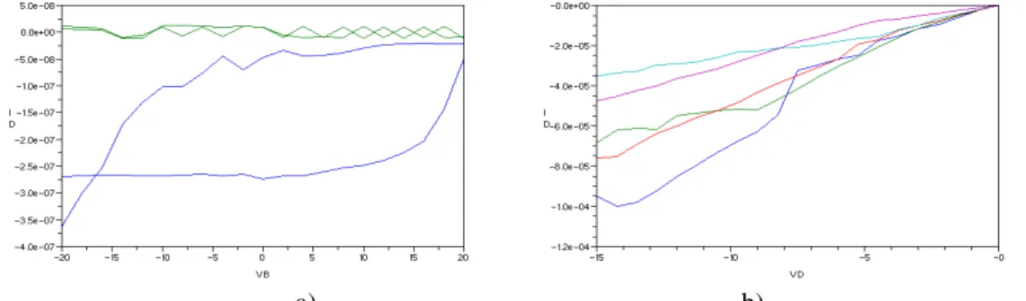
The room temperature transfer and current-voltage characteristics of the device under test are shown in Fig. 1. The ON/OFF observed from the transfer characteristics is about 20 which indicates presence a small amount of metallic nanotubes in the CNT film. The ON/OFF ratio observed from the current-voltage characteristics at high VDS is smaller due to drain induced
Schottky leakage [2,3].
Fig. 2 shows the transfer and current-voltage characteristics at 100°C. The characteristics in Fig. 2 present two effects: The reduction in film mobility and a slight increase in the Schottky barrier leakage at high drain bias. The transfer characteristics in Fig. 2(a) exhibits a reduced ON/OFF ratio due to reduced ON current which indicates reduced carrier mobility in the CNT film. The OFF current in Fig. 2(a) is not changed significantly with respect to its room temperature value. However, in Fig 2(b), an increase in the OFF current at high VDS can still be
clearly observed. Thus, we can conclude that, at 100°C, increased temperature results in increased thermally assisted injection through the Schottky barrier only when the drain bias is large. It needs to be noted that the current voltage characteristics in Fig. 2(b) is noisy, possibly due to interference from the heating setup.
Fig. 3 shows the transfer and current-voltage characteristics at 200°C. It can be seen that the ON/OFF ratio indicates the device to be inoperational. However the mechanism of the reduction of ON/OFF ratio is different: From Fig. 3(a), at 200°C the ON/OFF ratio is reduced due to an increase in the OFF current. It is interesting to note that the ON current is also increased beyond its room-temperature value. This increase in the current levels can also be observed in the current-voltage characteristics in Fig. 3(b). We suggest that the increase in the current levels and the weak modulation at 200°C can be attributed to thermally assisted injection from the Schottky
ISDRS 2009, December 9-11, 2009, College Park, MD, USA
ISDRS 2009 – http://www.ece.umd.edu/ISDRS2009
contacts increased to the extend that the gate modulation of the Schottky barrier is rendered ineffective.
At 300°C the device failed by exhibiting an open channel (no current) due to oxidation of the CNT film. This temperature is consistent with the thermogravimetric characterization of single wall CNTs which commonly shows complete oxidation at 300°C.
As a result, we have demonstrated that CNT-TFT can be employed for elevated temperature applications if the temperature is limited to below 100°C and the drain bias is kept small. The authors wish to acknowledge support from TUBITAK projects 106E049, 108E123, and 109E001.
References:
[1] H. Dai, “Carbon Nanotubes: Synthesis, Integration and Properties”, Acc. Chem. Res., vol. 35, pp. 1035-1044, 2002.
[2] M. Radosavljevic, S. Heinze, J. Tersoff,and Ph. Avouris, “Drain voltage scaling in carbon nanotube transistors,” Appl. Phys. Lett., vol. 83, no. 12, pp. 2435-2437, Sept., 2003. [3] T. Yamada, “Modeling of carbon nanotube Schottky barrier modulation under oxidizing
conditions,” Phys. Rev. B., vol. 69, paper 125408, 2004.
a) b)
Fig. 1 Transfer (a) and current-voltage (b) characteristics of the CNT-TFT under study at room temperature. In (a) the green curve is the gate current.
a) b)
Fig. 2 Transfer (a) and current-voltage (b) characteristics of the CNT-TFT under study at 200°C
a) b)