MID-INFRARED QUANTUM CASCADE
LASER
A THESIS SUBMITTED TO
THE GRADUATE SCHOOL OF ENGINEERING AND SCIENCE OF BILKENT UNIVERSITY
IN PARTIAL FULFILLMENT OF THE REQUIREMENTS FOR THE DEGREE OF
MASTER OF SCIENCE IN
ELECTRICAL AND ELECTRONICS ENGINEERING
By
Berkay Bozok
ii
MID-INFRARED QUANTUM CASCADE LASER By Berkay Bozok
May 2017
We certify that we have read this thesis and that in our opinion it is fully adequate, in scope and in quality, as a thesis for the degree of Master of Science.
Ekmel Özbay (Advisor)
Bayram Bütün (Co-Advisor)
Vakur Behçet Ertürk
Hamza Kurt
Approved for the Graduate School of Engineering and Sciences:
Ezhan Karaşan Director of Graduate School
iii
ABSTRACT
MID-INFRARED QUANTUM CASCADE LASER
Berkay Bozok
M.S. in Electrical and Electronics Engineering Advisor: Ekmel Özbay & Bayram Bütün
May 2017
Mid-infrared quantum cascade laser technology has been developed rapidly since it was demonstrated in 1994. Since quantum cascade laser technology is small, robust and efficient, they have become commonly used mid-infrared laser source for various applications. The particular application fields of quantum cascade lasers are free space communication, chemical spectroscopy, environmental monitoring and infrared countermeasure.
This work presents a comprehensive study over mid-infrared quantum cascade laser including review of theoretical background, theoretical analyses, active layer design, quantum mechanical, thermal and optical simulations, device fabrication, optimization and experimental characterization.
As a result of this work mid-infrared quantum cascade laser have been successfully demonstrated.
Keywords: Laser, Mid-infrared, MWIR, Quantum cascade laser, QCL,
iv
ÖZET
ORTA KIZILÖTESİ KUANTUM ÇAĞLAYAN LAZER
Berkay Bozok
Elektrik ve Elektronik Mühendisliği, Yüksek Lisans Tez Danışmanı: Ekmel Özbay & Bayram Bütün
Mayıs 2017
Orta kızılötesi kuantum çağlayan lazer teknolojisi, 1994 yılında icadından beri hızla gelişmiştir. Kuantum çağlayan lazer teknolojisi küçük, karmaşık olmayan ve verimli olduğundan, çeşitli uygulamalar için en çok kullanılan orta kızılötesi lazer kaynağı haline gelmiştir. Kuantum çağlayan lazerlerinin özel uygulama alanları serbest alan iletişimi, kimyasal spektroskopi, çevresel izleme ve kızılötesi karşı önlemlerdir.
Bu çalışma teorik arka plan incelemesi, teorik analizler, kuantum çağlayan lazer tasarımı, kuantum mekanik, termal ve optik simülasyonlar, cihaz imalatı, optimizasyonu ve deneysel karakterizasyonu içeren orta kızılötesi kuantum çağlayan lazeri üzerinde kapsamlı bir analiz sunmaktadır.
Bu çalışma sonucunda orta kızılötesi kuantum çağlayan lazer başarıyla geliştirilmiş ve üretilmiştir.
Anahtar Sözcükler: Lazer, Orta kızılötesi, Kuantum çağlayan lazer, KÇL,
v
Acknowledgements
I would like to thank my supervisor Prof. Dr. Ekmel Özbay and my co-supervisor Dr. Bayram Bütün. They provided me with invaluable guidance, suggestions and motivation during this work. Indeed I am thankful to Dr. Bayram Bütün for his patience and for being willing to discuss the problems arising from my life and research.
I would also like to thank Prof. Dr. Vakur B. Ertürk and Prof. Dr. Hamza Kurt for being on my thesis committee and evaluating my thesis.
This work would not be possible without good colleagues and friends. First, I would also thank all the past and present members of the NANOTAM. Especially, I would like to thank Doğan Yılmaz and Gökhan Mehmetoğlu for their friendships, their invaluable support and work for this thesis. I would also like to thank NANOTAM opto-electronic team; Dr. Deniz Çalışkan, Deniz Gülcü, Ramazan Özsoy, Tolga Şenol and Okan Ateşal.
Also I want to thank present and past members of Demir research group, where I have started doing science. Especially, I would like to thank Can Uran and Shahab Akhavan from whom I have learned my basic lab skills.
Finally, I would like to thank my family, my grandmother Şükran, my grandfather Abuzer, my mother Zerrin, my father İsmail, my uncle Erkan and my cousin Hakkı for their love, support and encouragement.
vi
Contents
1 Introduction 1
1.1. Mid-Infrared Applications ... 2
1.2. Mid-Infrared Sources ... 4
1.3. Intersubband Transitions and Quantum Cascade Lasers ... 5
1.4. Material Systems ... 8
1.5. Thesis Overview ... 10
2 Intersubband Laser Theory and Modeling 11
2.1. Fundamentals ... 11
2.1.1. Single Quantum Well ... 12
2.1.2. Coupled Well Systems ... 13
2.1.3. Superlattice ... 16
2.2. Intersubband Electronic States ... 18
2.3. Intersubband Transitions ... 21
2.3.1. Interaction Hamiltonian ... 21
2.3.2. Selection Rule: The Origin of Polarization Behavior ... 23
2.3.3. Intersubband Radiative Transitions ... 24
2.4. Nonradiative Inter-subband and Intra-subband Transitions ... 26
2.4.1. Spontaneous Emission ... 27
2.4.2. Phonon Scattering ... 28
vii
2.5. Quantum Cascade Laser Rate Equation ... 32
2.6. Gain Medium Design and Modeling ... 35
2.6.1. Active Region Design ... 36
2.6.2. Injection Region Design ... 39
2.6.3. Cascading ... 43
2.7. Active Layer Design and Modeling ... 44
2.8. Thermal Design and Modeling ... 46
2.9. Mid-Infrared Waveguides, Design and Modeling ... 51
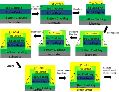
3 Device Fabrication and Packaging 58
3.1. Epitaxial Growth ... 58
3.2. Cleanroom Fabrication ... 59
3.2.1. Wafer Cleaving and Sample Cleaning ... 61
3.2.2. Top Contact Lithography ... 61
3.2.3. Top Contact Deposition ... 63
3.2.4. Mesa Lithography ... 65
3.2.5. Mesa Etching ... 66
3.2.6. Dielectric Coating ... 70
3.2.7. Dielectric Opening ... 71
3.2.8. Seed Metal Lithography ... 73
3.2.9. Seed Metal Deposition ... 75
3.2.10. Electroplating Lithography ... 76
3.2.11. Electroplating ... 78
3.2.12. Lapping ... 79
viii
3.2.14. Mirror Coating and Device Mounting ... 81
3.2.15. Packaging ... 84
4 Device Characterization and Discussions 85
4.1. Measurement Setup ... 85
4.1.1. Temperature Dependent L-I-V Measurement ... 86
4.1.2. Spectrum Measurement ... 89
4.2. Results and Discussions ... 91
4.2.1. Temperature Dependent L-I-V ... 91
4.2.2. Spectrum ... 100
5 Conclusions 103
ix
List of Figures
1.1 a) Graphical representation of the location of strong absorptions of
molecules [1] b) Illustration of infrared countermeasures of an
aircraft [2]. ... 3
1.2 Schematic comparison of various mid-infrared laser sources [3]. ... 4
1.3 (a) Intersubband transition and gain spectrum, (b) interband transition and gain spectrum [3]. ... 6
1.4 Conduction band energy diagram of the first quantum cascade laser and corresponding energy levels. Energy level 3 is upper laser level, 1 and 2 are lower laser levels. Active region is region where laser action takes place and digitally graded alloy is region that superlattice structure exists [5]. ... 8
1.5 Conduction band and effective conduction band offset ... 8
2.1 Illustration of coupled well system and two un-coupled wells. ... 14
2.2 Illustration of superlattice potential. ... 17
2.3 (a) Illustration of intersubband optical phonon scattering process.(b) In-plane reciprocal lattice space illustration of the initial and final electron wavevectors ki and kf and their vector difference [17]. ... 30
2.4 Rate equation model illustration ... 32
2.5 Conduction band diagram of first quantum cascade laser [7]. ... 36
2.6 Vertical and diagonal transition comparison [3]. ... 37
x
2.8 Minibands/minigap design logic illustration. ... 41
2.9 Computed transition of superlattice structure with 3 and 5 number of
periods [3]. ... 42
2.10 Band structure and moduli squared of corresponding wave function under
an 83kV/cm electric field. Laser action happened between level 3 and
level 2. ... 44
2.11 Band structure and moduli squared of the corresponding wavefunctions
for one period of cascaded layers under applied electric field of 83 kV/cm.
Laser action occurs between level 3 and level 2,red (solid) line indicates
radiative transition. Electrons are relax from level 2 to level 1 and level 1
to level 0 by LO phonon scattering, black (dashed) arrow indicates
non-radiative transition. ... 45
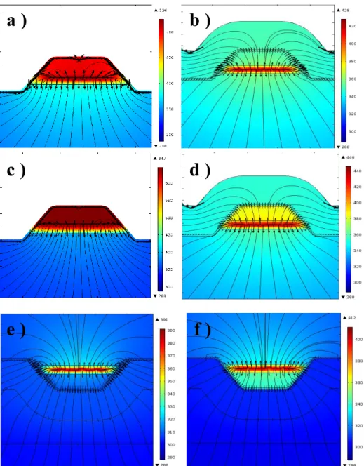
2.12 Total heat flux patterns and temperature distribution simulated for
conventional ridge waveguide quantum cascade lasers (a) passivated with
Si3N4 andwithout electroplated gold for epi-up bonding, and (b)
passivated with Si3N4 andwith 5 μm thick electroplated gold for epi-up
bonding, (c) passivated with SiO2 andwithout electroplated gold for
epi-up bonding, (d) passivated with SiO2 andwith 5 μm thick electroplated
gold for epi-up bonding, (e) passivated with Si3N4 andwith 5 μm thick
electroplated gold for epi-down bonding,(f) passivated with SiO2 andwith
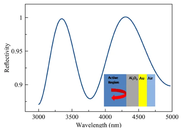
5 μm thick electroplated gold for epi-down bonding ... 50 2.13 FDTD simulation (Lumerical) of reflectivity of Al2O3/Au (100 nm/100
xi
2.14 Waveguide design illustration of fabricated device ... 55
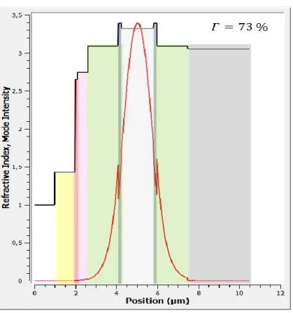
2.15 Fundamental TM mode intensity and refractive index of the vertical waveguide at 4.5 μm wavelength. ... 56
2.16 (a) Used FDTD model and (b) simulation result of fundamental TM mode profile. ... 57
3.1 Schematic illustration of molecular beam epitaxy (MBE) system []. ... 59
3.2 Schematic diagram of ridge quantum cascade laser fabrication process. . 60
3.3 Top contact lithography mask. ... 62
3.4 Optical microscope image (20x optical zoom) after top contact lithography an development. ... 63
3.5 Optical microscope (5x optical zoom) image after metal deposition and annealing. ... 64
3.6 Mesa Lithography photomask. ... 65
3.7 Optical microscope (5x optical zoom) image after development... 66
3.8 Optic microscope images after wet etching. ... 67
3.9 SEM image of quantum cascade laser after wet etch. ... 67
3.10 SEM image of quantum cascade laser after dry etch. ... 69
3.11 SEM image of mushroom like quantum cascade laser. ... 69
3.12 Lumerical optic loss simulation with different passivation material and thickness. ... 71
3.13 Photomask for dielectric opening lithography. ... 72
3.14 Optical microscope image after Si3N4 deposition and opening. ... 72
xii
3.16 Cross section scanning electron microscopy image of quantum cascade
laser deposited thick metal without patterning. ... 74
3.17 Photomask for seed metal lithography. ... 75
3.18 Photomask for electroplating lithography. ... 76
3.19 Optical microscope image after electroplating lithography and development. ... 77
3.20 Electroplating setup. ... 78
3.21 Scannig electron microscop image after thick metal deposition. ... 79
3.22 Separated laser bars and remained substrate. ... 80
3.23 Reflectivity of the mirror which consists of 5 nm Ti and 100 nm Au with varying Al2O3 thickness. ... 82
3.24 Schematic illustration of mirror coating process. ... 83
3.25 Optic microscope images after mirror coating process. ... 83
3.26 Completed quantum cascade laser devices’ photography and SEM image. ... 84
4.1 LIV measurement setup. ... 86
4.2 Illustration of current pulse applied on quantum cascade laser... 87
4.3 Schematic illustration of optical power-current-voltage (LIV) measurement setup. ... 88
4.4 Optical spectrum analyzer used for spectrum measurement. ... 89
xiii
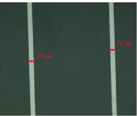
4.6 The optical power – current measurement (1% duty cycle) for device for which waveguide length is 4 mm and ridge width is 20 μm at different temperatures. Temperature dependent threshold current density and
characteristic temperature (T0) is shown... 91
4.7 The optical power – current measurement (1% duty cycle) for device for which waveguide length is 4 mm and ridge width is 20 μm at different temperatures. Temperature dependent threshold current density and
characteristic temperature (T0) is shown... 92
4.8 The optical power – current measurement (20% duty cycle) for device for which waveguide length is 4 mm and ridge width is 16 μm at different temperatures. ... 93
4.9 The optical power – current measurement (1% duty cycle) for devices which are 4 mm length and 20 μm width without mirror coating, 2 mm length and 20 μm width without mirror coating and 2 mm length and 20 μm width with mirror coating at room temperature. ... 94 4.10 The optical power – current measurement (1% duty cycle) for device for
which waveguide length is 2 mm and ridge width is 20 μm at different temperatures. Temperature dependent threshold current density and
characteristic temperature (T0) is shown... 95
4.11 The optical power – current measurement (1% duty cycle) for device for which waveguide length is 2 mm and ridge width is 16 μm at different temperatures. Temperature dependent threshold current density and
xiv
4.12 The optical power – current measurement (20% duty cycle) for device for which waveguide length is 2 mm and ridge width is 20 μm at different temperatures. ... 96
4.13 The optical power – current measurement (20%, 30%, 40% and 50% duty
cycle) for device for which waveguide length is 2 mm and ridge width is 20 μm at room temperature. ... 97 4.14 Temperature dependent slope efficiency (1% duty cycle) of devices for
which waveguide length is 2 mm and ridge width is 20 μm with mirror coating, waveguide length is 2 mm and ridge width is 16 μm with mirror coating, waveguide length is 4 mm and ridge width is 16 μm without mirror coating and waveguide length is 4 mm and ridge width is 20 μm
without mirror coating. ... 98
4.15 Current – Voltage (I-V) measurement (1% duty cycle) for device for
which waveguide length is 2 mm, 4 mm and ridge width is 20 μm at room
temperature. ... 99
4.16 Lasing spectrum of the device whose length is 4 mm and width is 20 μm
is operated in pulse mode at different temperatures. ... 100
4.17 Lasing spectrum of the device whose length is 4 mm and width is 20 μm
xv
List of Tables
2.1 Thermal conductivities of materials that is used in the simulation……….………...……49
1
Chapter 1
1.
Introduction
Laser (Light Amplification by Stimulated Emission of Radiation) devices are very important light sources and they have found various applications. Lasers are optical oscillators and they consist of two parts; optical amplifier and optical feedback element. Amplification is provided by stimulated emission and optical feedback is achieved by optical resonators (cavities). Semiconductor lasers are widely used and commercialized for violet to near-infrared spectrum. However it is very hard to achieve longer wavelengths such as mid-, far-infrared and terahertz with conventional semiconductor lasers.
The quantum cascade laser technology can completely satisfy the requirement of long wavelength semiconductor laser source. Quantum cascade lasers are based intersubband electron transition instead of electron-hole recombination as conventional semiconductor lasers do. Since intersubband transition energy is independent of material band gap, and it can be engineered by changing material thickness, essentially any wavelength can be obtained by quantum cascade lasers
2
1.1. Mid-Infrared Applications
Coherent mid-infrared source has found large number of applications;
Chemical spectroscopy and environmental monitoring: Most chemical molecules have special absorptions fingerprints in mid-infrared spectrum because of their chemical bonding vibrational transition in infrared. Therefore mid-infrared lasers can be used as spectroscopy source and environmental monitoring. Graphical representation of the location of absorptions of some molecules in infrared spectrum is presented in Figure 1.1 (a).
Free space communication: Since water vapor does not have absorption in infrared, atmosphere is almost transparent for infrared light. Therefore mid-infrared lasers can be used for long range free space communication and light detection and ranging (LIDAR).
Infrared countermeasure: It is important military application. It is possible to confuse heat-seeking missiles guidance systems by mid-infrared source in order to protect aircrafts. Illustration of infrared countermeasures of an aircraft is presented in Figure 1.1 (b).
3
Figure 1.1 Figure 1.1 a) Graphical representation of the location of strong absorptions of molecules [1] b) Illustration of infrared countermeasures of an aircraft [2].
a)
4
1.2. Mid-Infrared Sources
A schematic comparison of various mid-infrared laser sources is presented in Figure 1.2 [3].
Figure 1.2 Schematic comparison of various mid-infrared laser sources [3].
CO and CO2 lasers can be mid-infrared laser sources but their emission
wavelength is fixed and tunability is not possible, also they are expensive and bulky. Fiber lasers are being used for non-linear down conversion to produce mid-infrared laser light but this technique is very complex and expensive. Conventional semiconductor lasers based on GaInSb/InAlSb or AlSb material can be used as mid-infrared laser sources but they operate at cryogenic temperatures only. IV-VI lead salt lasers are also possible for mid-infrared laser source but it requires cryogenic temperatures for operation and its output power is very low. However quantum cascade lasers can operate at room temperature, their emission wavelength can be widely tunable with high optical power, they are not too expensive and complex; therefore they are very attractive for number of mid-infrared applications.
5
1.3. Intersubband Transitions and Quantum
Cascade Lasers
The main difference between conventional semiconductor lasers and quantum cascade lasers is conventional semiconductor lasers based on electron transition between conduction band to valence band whereas quantum cascade lasers are unipolar devices, which means laser beam is generated by the electron transition in conduction band only. The realization of the quantum cascade devices requires nanometer accuracy epitaxial growth. Very thin and smooth quantum well structures are needed. When these quantum wells are thin below the de-Broglie wavelength of electrons in semiconductor, quantum states which are controlled by confinement are formed. Therefore it is possible to create upper and lower laser levels in conduction band with these thin quantum well structures.
The joint density of states is different for interband and intersubband transitions. Therefore optical behaviors of interband and intersubband transitions are very different. The joint density of states in interband transition is characterized by electron and hole distribution in conduction and valence band respectively. Therefore gain spectrum of interband transition is broadened naturally. In contrast, the joint density of states in intersubband transition is delta like [3], so transition is very similar to atomic systems. Gain spectrum is less broadened than interband transitions. Schematic illustration of optical transition and gain spectrum of intersubband and interband transitions are presented in Figure 1.3.
6
Figure 1.3 (a) Intersubband transition and gain spectrum, (b) interband transition and gain spectrum [3].
In 1971, Kazarinov and Suris [4] demonstrate that light amplification is possible with a transition between two intersubband states in a semiconductor. They demonstrate that electron can tunnel from the ground state of the quantum well to excited state of neighboring well by emitting photon, which process is called “photon assisted tunneling”. Also this process can be repeated many times by cascading quantum wells. However, they could not achieve gain. Since when several quantum wells are cascaded (without doping), due to space charge domain formation, electric field cannot be uniform in the structure and structure become electrically unstable [5]. J.Faist and F.Capasso solved this electrical instability problem by adding injector regions (some of them are doped) between Kazarinov’s and Suris’s active region and they proposed first quantum cascade
7
laser in 1994 [7]. These injector states behaves as if electron reservoir to prevent space charge domain formation and provide uniform electric field across the device.
Similar for all kind of laser systems, quantum cascade laser also consist of two parts; gain medium and optical resonator. Optical resonator can be simply formed by micro fabrication techniques and it is very similar to conventional semiconductor lasers. However gain medium of quantum cascade lasers are very different than conventional semiconductor lasers. It is possible to divide gain medium as active region where laser transition occurs and injection region where electron pumped to following active region.
Active region consists of thin quantum wells. Since these quantum wells are thin enough due to quantum confinement discrete energy levels are formed. These discrete energy levels are upper and lower laser states. Additionally laser wavelength can be controlled by changing the thickness of these quantum wells. Injection region is a superlattice structure. As Esaki and Tsu [6] point out first that artificial miniband and minigap structures can be created by forming periodic quantum wells. Sequence of quantum well layers can behave as one dimensional crystal structure; they form artificial band and band gaps. This injection region pumps electron to upper laser levels and discharge electron from lower laser levels. They are used as to create cascade structure, in other words active regions can be combined by injection regions to create cascaded structure.
The first quantum cascade laser are made by J.Faist and F.Capasso in 1994 in Bell Labs [7]. It is operated at wavelength of 4.2 µm and it could lase only in pulse mode at cryogenic temperatures with 14 kA/cm2. The very first quantum
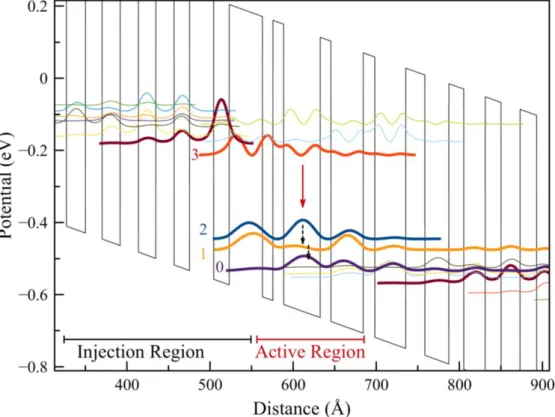
cascade laser gain medium band structure is presented in Figure 1.4. The active part consist of three coupled quantum wells, there is three level laser system in which population inversion between level 2 and 3 is obtained.
8
Figure 1.4 Conduction band energy diagram of the first quantum cascade laser and corresponding energy levels. Energy level 3 is upper laser level, 1 and 2 are lower laser levels. Active region is region where laser action takes place and digitally graded alloy is region that superlattice structure exists [7].
1.4. Material Systems
In this work InGaAs/AlInAs/InP material system is used to realize quantum cascade laser. However other heterostructures material systems (Figure 1.5) are also possible for quantum cascade lasers.
9
Lattice matched InGaAs/AlInAs/InP material system has 0.52 eV band discontinuities, so it allows minimum 4.3 μm wavelengths. Furthermore, electron effective mass of InGaAs/AlInAs/InP material system is small (𝑚 ≈ 0.043𝑚0) [15] almost half of the GaAs/AlGaAs material system, which allows to use larger quantum well width and make thickness fluctuations less critical (since optical matrix element inversely proportional to effective mass). Non-radiative relaxation time is also larger since 𝜏~ 1 √𝑚⁄ , therefore gain is larger than GaAs/AlGaAs material system, because gain is also inversely proportional to effective electron mass. Additionally refractive index of InP is less than InGaAs an InAlAs; hence forming cladding layer is also straightforward. It is also possible to increase conduction band discontinuity by strain compensation in order to obtain shorter wavelengths (minimum possible is 3.05 μm).
Due to higher electron effective mass comparing to InGaAs/AlInAs/InP material system, GaAs/AlGaAs material systems has lower gain. However GaAs/AlGaAs material systems has lower free-carrier losses (since free carrier loss is inversely proportional to electron effective mass). Therefore GaAs/AlGaAs material system is very promising for longer wavelengths especially THz lasers.
InAs/AlSb material system is very promising for short wavelength quantum cascade lasers and it has very low electron effective mass (𝑚 ≈ 0.023𝑚0), so
gain should be 2.5 times higher than InGaAs/AlInAs/InP material system [15]. However forming waveguide is very challenging because refractive index of active layer and cladding layers are the same. Also epitaxy growth of InAs/AlSb material systems is harder than InGaAs/AlInAs/InP material system.
There is also Si/SiGe material system for quantum cascade lasers but in this case laser transition occurs in valance band instead of conduction band. This material system is very promising for silicon-based integrated optic. However, there is no Si-based quantum cascade laser has been reported so far, intersubband electroluminescence was reported only in 2000 and 2002 [8,9].
10
1.5. Thesis Overview
The objective of this work is the developed quantum cascade laser which emits laser beam in between 4 µm to 5 µm wavelength and it must be operated above 50 mW optical power under 1% pulsed operation and it must be operated in continuous mode with minimum 5 mW optical power at room temperature. This thesis organized as follows: in Chapter 2, the basic theory behind the quantum cascade laser is discussed. In particular, elementary quantum mechanics, formation of intersubband electronic states, radiative and non-radiative transitions are described. Theoretical backgrounds are explained to design quantum cascade laser, design methodology of quantum cascade lasers are mentioned, thermal and optical behavior of the quantum cascade lasers are analyzed and simulation results are presented.
In Chapter 3 overview of ridge waveguide fabrications process are presented in detail and fabrication development processes are mentioned. Different waveguide formation techniques are discussed and their effects on device performance are analyzed.
Chapter 4 covers characterization results of the fabricated quantum cascade laser are analyzed. Temperature dependent optical powers with different duty cycles and under different bias conditions are measured. Performance parameters; characteristic temperature, threshold current density and slope efficiencies are analyzed. Spectrum of laser is also measured at different temperatures and under different bias conditions.
11
Chapter 2
2.
Intersubband Laser Theory and
Modeling
In this chapter, the essential background to design mid-infrared quantum cascade lasers is reviewed. Basic quantum mechanics including single quantum well solutions, coupled well systems, superlattice structures and intersubband electronic states are reviewed. Intersubband optical processes both radiative and nonradiative transitions are reviewed and their effects on device performance are discussed. Active region design parameters and conduction band engineering tools to design quantum cascade laser are presented. Macroscopic laser rate equations are derived for quantum cascade laser and performance parameters such as threshold current density and slope efficiency equations are obtained. Finally, thermal and optical design parameters are discussed.
2.1. Fundamentals
In this section fundamental quantum mechanics is reviewed to understand how quantum cascade laser works. Single quantum well solutions, coupled well systems, superlattice structures and intersubband electronic states are reviewed.
12
2.1.1. Single Quantum Well
Single quantum well problem is easy and a fundamental problem in quantum mechanics. Even if single quantum well problem is not used directly in quantum cascade laser design, it is a good starting point. In addition to that single quantum well problem is routinely used in some modern optoelectronic devices such as electro-absorption modulators and semiconductor interband lasers. The simplest form of single quantum well problem is one dimensional quantum well with infinite barriers. Consider particle with mass m with spatially varying potential V (z).
𝑉(𝑧) = {0 𝑖𝑓 0 ≤ 𝑧 ≤ 𝐿𝑍
∞ 𝑜𝑡ℎ𝑒𝑟𝑤𝑖𝑠𝑒} , (2.1)
where Lz is quantum well width. In order to solve this problem (time-independent) Schrödinger equation is solved and equate boundary conditions. Since energy is infinite at the edges of the quantum well, it is safely say, wavefunction is zero at the edges. So Schrödinger equation in the well is
− ħ2
2m d2Ψ(z)
dz2 = EΨ(z), (2.2)
where Ψ(z) is wavefunction, z is growth direction, E is energy eigenvalue and subject to the boundary conditions at the edges. Solution to (2.2) is simple
𝛹(𝑧) = 𝐴𝑠𝑖𝑛(𝑘𝑧) + 𝐵𝑐𝑜𝑠(𝑘𝑧), (2.3)
where A and B are constants and according to boundary condition B=0 and
k=√2𝑚𝐸⁄ . Hence the solution of this equation is, ħ2
𝛹(𝑧) = 𝐴𝑛𝑠𝑖𝑛 (𝑛𝜋𝑧
𝐿𝑧), (2.4)
Where An is normalization constant which is√2 𝐿
𝑧
⁄ . Associated energies are
𝐸𝑛 = ħ2 2𝑚( 𝑛𝜋𝑧 𝐿𝑧 ) 2 . (2.5)
13
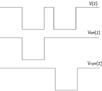
More realistic picture of single quantum well is finite barrier quantum well. In this case potential of outside is not infinite, it is finite and for simplicity it is constant. Let spatially varying potential V (z) as;
𝑉(𝑧) = {−𝑉𝑏 𝑖𝑓 −𝐿𝑧⁄ ≤ 𝑧 ≤ 𝐿2 𝑧⁄2
0 𝑜𝑡ℎ𝑒𝑟𝑤𝑖𝑠𝑒 }. (2.6)
In this case, it is known that nature of the solution in the outside the well is exponential and in the well solution is sinusoidal. Therefore wave function must be; 𝛹(𝑧) = { 𝐺𝑒𝜅𝑧, 𝑧 ≤ −𝐿𝑧 2 ⁄ 𝐴𝑠𝑖𝑛(𝑘𝑧) + 𝐵𝑐𝑜𝑠(𝑘𝑧), −𝐿𝑧 2 ⁄ ≤ 𝑧 ≤ 𝐿𝑧 2 ⁄ < 0 𝐺𝑒−𝜅𝑧, 𝑧 ≥𝐿𝑧 2 ⁄ ≥ 0 (2.7)
In this case solution is trivial after applying boundary conditions, which is continuity of wavefunction. However analytical solution is not possible, graphically wavefunctions and associated energy levels can be found [10].
2.1.2. Coupled Well Systems
The coupled well system can be considered as two finite quantum well coupled thought a barrier. This problem can be solved directly by calculating Hamiltonian of the whole system. However it requires cumbersome mathematical procedures. Instead of solving Hamiltonian directly, tight binding model is much more useful [11]. Perturbation theory, especially finite basis set approach can be used to approximate starting basis function [10]. Consider two infinite well as separately and define wavefunctions and potentials as 𝛹(𝑧)𝑟𝑖𝑔ℎ𝑡 and 𝑉(𝑧)𝑟𝑖𝑔ℎ𝑡 for well on the right ,𝛹(𝑧)𝑙𝑒𝑓𝑡 and 𝑉(𝑧)𝑙𝑒𝑓𝑡 for left well. Let V(z) is the potential of the coupled system, which is 𝑉(𝑧) = 𝑉(𝑧)𝑙𝑒𝑓𝑡+ 𝑉(𝑧)𝑟𝑖𝑔ℎ𝑡 .
14
Figure 2.1 Illustration of coupled well system and two un-coupled wells.
Hamiltonian of this system is
Ĥ = − ħ2
2𝑚 𝑑2
𝑑𝑧2+ 𝑉(𝑧)𝑙𝑒𝑓𝑡+ 𝑉(𝑧)𝑟𝑖𝑔ℎ𝑡. (2.8)
As long as barrier is reasonably thick, it can be approximated that wavefunctions in the wells are tightly combined, in other words, leakage of the wavefunction to adjacent well is negligible. With this approximation, wavefunctions are considered as approximately orthogonal and they can be used as basis for coupled system and wavefunction of the coupled system is:
𝛹(𝑧) = A𝛹(𝑧)𝑙𝑒𝑓𝑡+ 𝐵𝛹(𝑧)𝑟𝑖𝑔ℎ𝑡. (2.9)
In the matrix form of finite basis approximation of coupled well Schrödinger equation is: [𝐻𝐻11 𝐻12 21 𝐻22] [ 𝐴 𝐵] = 𝐸 [ 𝐴 𝐵]. (2.10)
15 Hamiltonians can be given explicitly as;
𝐻11 = ∫ 𝛹(𝑧)𝑙𝑒𝑓𝑡∗ (− ħ2 2𝑚 𝑑2 𝑑𝑧2+ 𝑉(𝑧)𝑙𝑒𝑓𝑡+ 𝑉(𝑧)𝑟𝑖𝑔ℎ𝑡) 𝛹(𝑧)𝑙𝑒𝑓𝑡, (2.11) and 𝐻22= ∫ 𝛹(𝑧)𝑟𝑖𝑔ℎ𝑡∗ (− ħ2 2𝑚 𝑑2 𝑑𝑧2+ 𝑉(𝑧)𝑙𝑒𝑓𝑡+ 𝑉(𝑧)𝑟𝑖𝑔ℎ𝑡) 𝛹(𝑧)𝑟𝑖𝑔ℎ𝑡. (2.12)
Since we assume leakage of the wavefunction to adjacent well is negligible 𝐻11≈ 𝐸1 and 𝐻22 ≈ 𝐸1 where 𝐸1 is associated ground energy of uncoupled well.
However interaction of the wavefunction in the barrier cannot be completely negligible and this interaction appears in 𝐻21 and 𝐻12 terms, they are:
𝐻21∗ = 𝐻12 = ∫ 𝛹(𝑧)𝑙𝑒𝑓𝑡∗ (−
ħ2
2𝑚 𝑑2
𝑑𝑧2) 𝛹(𝑧)𝑟𝑖𝑔ℎ𝑡. (2.13)
Additionally this Hamiltonians can be defines as splitting energy (∆𝐸).
With these assumptions and simplifications, matrix form of Schrödinger equation is: [𝐸1 ∆𝐸 ∆𝐸∗ 𝐸 1] [ 𝐴 𝐵] = 𝐸 [ 𝐴 𝐵]. (2.14)
In order to find energy eigenvalues, determinant of (2.14) should be zero;
|𝐸1 − 𝐸 ∆𝐸 ∆𝐸∗ 𝐸
1− 𝐸| = 0, (2.15)
and obtaining eigenvalues;
𝐸 = 𝐸1± ∆𝐸, (2.16) and normalized wavefunctions are;
𝛹(𝑧) = √1
2(𝛹(𝑧)𝑙𝑒𝑓𝑡± 𝛹(𝑧)𝑟𝑖𝑔ℎ𝑡). (2.17)
As given in Figure 2.1 wavefunction consists of symmetric and anti symmetric combinations of single quantum well solution. Since normalization constant is same for right and left, electron equally exist in both wells. These states are
16
separated by energy difference of ∆𝐸. Actually, this is a common phenomenon in quantum mechanics, it is mostly observed in solid-state physics; when two atoms are brought closer, they have a tendency to form energy bands of very closely spaced energy states rather than discrete energy levels. This phenomenon can also be observed when quantum wells are brought together; they form an artificial energy band, which kind of systems calls superlattice, which will be covered in detail in the next subsection.
2.1.3. Superlattice
As it is discussed in previous subsection, it is possible to create artificial band gaps by bringing quantum wells closely together. These structures are called superlattice. Suppose in the superlattice potential is
𝑉(𝑧) = ∑∞𝑛=−∞𝑉𝑤(𝑧 − 𝑛𝑙). (2.18)
where Vw is
𝑉𝑤(𝑧 − 𝑛𝑙) = {−𝑉𝑏 𝑖𝑓 |𝑧 − 𝑛𝑙| ≤ Lz⁄2
0 𝑖𝑓 |𝑧 − 𝑛𝑙| ≥ Lz⁄2}. (2.19)
where n is an integer. As it is also understood from the potential definition, it is not possible to create such a potential in practice, since n spans minus infinity to infinity. However it is not too wrong to approximate as if it is infinite [10]. Wavefunctions in the well and in the barrier is:
𝛹(𝑧) = { 𝐴𝑒
ikw(z−nl)+ 𝐵𝑒−ikw(z−nl), |𝑧 − 𝑛𝑙| < L z⁄2
𝐶𝑒ikB(z−nl−2l)+ 𝐷𝑒−ikB(z−nl−2l), |𝑧 − 𝑛𝑙| < h 2⁄ . (2.20)
17 Figure 2.2 Illustration of superlattice potential.
Since structure is periodic, boundary conditions have to obey Bloch theorem that is
𝛹𝑞(𝑧 + 𝑛𝑙) = 𝛹𝑞(𝑧)eiqnl. (2.21)
where l is periodicity and q is an integer. After applying boundary condition solution of this potential system is
cos(𝑞𝑙) = cos(kw𝐿) cos(kBh) −1
2( kB kw−
kw
kB) sin(kwL) sin(kBh) (2.22)
The (2.22) completely defines dispersion relation between q and energy, which is the origin of artificial energy bands [3]. This artificial energy bands are called mini-band and artificial energy gaps are called mini-gap in literature. It is possible to adjust energy levels of minigaps and minibands by just changing barrier and/or well thicknesses. Supperlattices are very useful in quantum cascade design especially injection/relaxation design. Because superlattice structure provide confinement for upper laser states whereas allow efficient tunneling for lower laser states.(This phenomena discuss in “Active Region Design” chapter in detail.)
18
2.2. Intersubband Electronic States
The quantum cascade lasers are composed of atomically abrupt layers. Layers are composed of alternating materials that have different electron affinities. This electron affinity difference forms a sharp band edge difference, which creates quantum wells and barriers in conduction band. In addition since layer thicknesses are in the order of de Broglie wavelength, energy stares are quantized along to the growth direction (conventionally this direction is assigned as z direction ). The effective mass theorem and envelope function approximation is very useful to obtain wavefunctions and energy bands of that kind of structure. Indeed it is possible to solve this structure without any approximation such as its band can be solved by “ab inito” quantum chemistry method but such a computation is very time consuming and it will not add any significant correction to envelope approximation [3].
According to the effective mass theorem, envelope function approximation, and because of in-plane (x and y directions) translational invariance wavefunction of the electron in this structure can be written in cylindrical coordinates as;
𝛹(𝑧) = 𝐹(𝑟)𝑈𝑛,0(𝑟). (2.23)
where F(r) is the envelope function and satisfies the effective mass equation and 𝑈𝑛,0 is Bloch function (n is index of considered band).
In addition a few approximations are made: envelope function is varying slowly compared to Bloch function, envelope function can be expressed as linear combination of other functions and Bloch function is identical in all layers. According to these assumptions and in-plane translational in variance, envelope function is;
𝐹(𝑟)𝑛,𝑘|| = 1
√𝑆||𝑒
𝑖𝑘||𝑟||Ӽ(𝑧)
19
where 𝑆|| is the normalization area, 𝑘|| is in plane wavevector and Ӽ(𝑧)𝑛 is nth wavevector. Hamiltonian of the system can be written in growth direction and assume that electron behaves as free particle in plane direction. First start with one-band model [12], in this model effective mass of electron just depends on conduction band (depends on bandgap only since Kane’s energy is much higher than bandgap), which is also known as parabolic effective mass model. In this model we ignore valence bands effects on effective mass. Hamiltonian according to this model is;
Ĥ = [− ħ
2 2𝑚(𝑧)
𝑑2
𝑑𝑧2+ V(z)] Ӽ(𝑧)𝑛. (2.25)
and corresponding Schrödinger equation is;
[− ħ
2 2𝑚(𝑧)
𝑑2
𝑑𝑧2+ V(z)] Ӽ(𝑧)𝑛 = 𝐸Ӽ(𝑧)𝑛. (2.26)
Note that effective mass is not position dependent in the same material in this model, however since material are different effective mass is also different in the wells and barriers. (2.26) can be solved easily with boundary conditions between interfaces (interface between material w and b for example);
Ӽ(𝑧)𝑛𝑤 = Ӽ(𝑧) 𝑛 𝑏. (2.27) 1 𝑚𝑤(𝑧) ∂Ӽ(𝑧)𝑛𝑤 ∂z = 1 𝑚𝑏(𝑧) ∂Ӽ(𝑧)𝑛𝑏 ∂z . (2.28)
The eigenvectors and eigenvalues of (2.26) with boundary conditions ((2.27) and (2.28)) are enough to characterize energy levels of quantum cascade lasers. However it is also possible to add valence bands effects on effective mass, this addition can be based on k-p theory [11], which includes eight band model; conduction band, light and heavy hole, split of valence bands and their spins.
20
However correction on effective mass (nonparabolicity effect) can be made much easier way based on empirical two-band model [13], which assumes valence band is only one band and calculate interaction between conduction band to calculate effective mass. According to this model, effective mass is energy dependent and effective mass is [14];
𝑚(𝐸) = 𝑚 [1 +2𝑚𝛾(𝐸−𝐸ħ2 𝑐)]. (2.29)
where m is effective mass from one-band model, Ec is conduction band energy, E
is corresponding band energy and 𝛾 is nonparabolicity parameter. After this correction to effective mass, conduction band is not parabolic, nonparabolic, and
E-k relation is
𝐸𝑐(𝑘) = 𝐸𝑐(0) +2𝑚(𝐸,𝑧)ħ2k2 . (2.30)
This correction does not add any complexity to our first model ((2.26)), only effective mass term changes. We consider one-band model again but considering valence band effect on effective mass and effective mass becomes energy dependent, this model is called effective one band model in literature[15].
There are additional factors affect the accuracy of energy states in quantum cascade lasers, which are space charge effect and electron-electron interaction due to high doping (Hartree potential). In the quantum cascade structure different energy states contain different electron population, which forms electrostatic potential that affect band profile. This can be easily modeled with Poisson equation [16]. Schrödinger equation (2.26) and Poisson equation are solved iteratively to obtain more accurate solution. Since electron density in quantum cascade lasers are low (generally about 1016 cm-2), space-charge effect is negligible and such an iterative solution is unnecessary [17]. Electron-electron interaction can be considering with Hartree potential. This can be modeled as adding potential to Hamiltonian (2.25) and solve this new Hamiltonian and
21
Poisson equation iteratively [3]. However since electron density is low, this correction is also ignorable.
2.3. Intersubband Transitions
Radiative and nonradiative transitions result intersubband laser phenomena. As it is well known in order to make a laser gain medium is required. Optical gain in quantum cascade laser provided by stimulated emission between intersubband electronic states, and electron movement through the device is provided by nonradiative transition.
2.3.1. Interaction Hamiltonian
Interaction between light and electron can be modeled by defining perturbation Hamiltonian. Optical field is strong enough to change electron occurrence probability in quantum states but it is not strong enough to create new states, therefore perturbation theory can be used to model optical interaction. [10] Hamiltonian with optical field can be written as;
Ĥ = Ĥ0+ Ĥint. (2.31)
where Ĥ0 is Hamiltonian of current state and Ĥint is perturbation Hamiltonian due to optical field. Interaction Hamiltonian can be derived from electromagnetic potential vector 𝐴⃗ as using coulomb gauge (or transverse gauge). Interaction Hamiltonian is;
Ĥint= (𝒑−𝑒𝑨)2
2𝑚 . (2.32)
22 Ĥint = −
𝑒
2𝑚 𝐴 ∙ 𝑝. (2.33)
where m is effective mass, which can be effective mass from-one band model or effective one band model. It is also possible to write this term with full band k-p model, in this case interaction Hamiltonian remains same but perturbation term will changes. In our discussion we will continue with one band or effective one band model. After defining interaction Hamiltonian, a perturbation term is;
〈𝛹(𝑧)𝑖|Ĥint|𝛹(𝑧)𝑓〉 = − 𝑒
𝑚〈𝛹(𝑧)𝑖|𝐴 ∙ 𝑝|𝛹(𝑧)𝑓〉. (2.34)
To make dipole approximation which assumes that light wavelength is too longer than wells dimensions so spatial dependency of A can be neglected in dot product, so perturbation term is:
〈𝛹(𝑧)𝑖|Ĥint|𝛹(𝑧)𝑓〉 = − 𝑒
𝑚𝐴〈𝛹(𝑧)𝑖|𝑝|𝛹(𝑧)𝑓〉. (2.35)
The vector potential A can be expressed as electromagnetic wave. Let electromagnetic field is;
𝐸⃗⃗ = 𝐸0cos(𝑘𝑟 − 𝑤𝑡) (𝑥̂ + 𝑦̂ + 𝑧̂). (2.36)
So vector potential is;
𝐴 =𝑖𝐸0
2𝑤(𝑥̂ + 𝑦̂ + 𝑧̂)𝑒
𝑖(𝑘𝑟−𝑤𝑡)+ 𝐶. (2.37)
Therefore perturbation term is;
〈𝛹(𝑧)𝑖|Ĥint|𝛹(𝑧)𝑓〉 = − 𝑒𝐸0
23
This term is essential to calculate absorption or gain coefficient.
2.3.2. Selection Rule: The Origin of Polarization
Behavior
Since quantum cascade laser emission based on intersubband electron relaxation, it has very unique property; stimulated emission (also absorption) is strongly polarized. If (2.28) is written explicitly (with using envelope approximation);
〈𝛹(𝑧)𝑖|(𝑥̂ + 𝑦̂ + 𝑧̂) ∙ 𝑝|𝛹(𝑧)𝑓〉 =
(𝑥̂ + 𝑦̂ + 𝑧̂) ∙ 〈𝑈𝑖,0|𝑝|𝑈𝑓,0〉 〈𝐹(𝑟)𝑖,𝑘|||𝐹(𝑟)𝑓,𝑘||〉 + (𝑥̂ + 𝑦̂ + 𝑧̂) ∙
〈𝑈𝑖,0|𝑈𝑓,0〉 〈𝐹(𝑟)𝑖,𝑘|||𝑝|𝐹(𝑟)𝑓,𝑘||〉. (2.39)
where i and f is initial band final states of band indices, since initial and final envelope functions are orthogonal first term in (2.29) vanishes. In the second term Bloch function is unity so only last part remains;
〈𝐹(𝑟)𝑖,𝑘|||(𝑥̂ + 𝑦̂ + 𝑧̂) ∙ 𝑝|𝐹(𝑟)𝑓,𝑘||〉 = 〈𝐹(𝑟)𝑖,𝑘|| 1 √𝑆||𝑒 𝑖𝑘||𝑟||Ӽ(𝑧) 𝑖|(𝑥̂ ∙ 𝑝̂ + 𝑦̂ ∙ 𝑝𝑥 ̂ + 𝑧̂ ∙ 𝑝𝑦 ̂)|𝑧 1 √𝑆||𝑒 𝑖𝑘||𝑟||Ӽ(𝑧) 𝑓〉. (2.40)
Contribution of x and y direction vanish; only z component remains. Therefore electromagnetic field (electric field in our case) interacting intersubband energy levels and propagating in plane direction (either x or y direction) has to be in z direction (growth direction), which means electromagnetic field which couples to the intersubband energy levels has to be TM polarized.
24
2.3.3. Intersubband Radiative Transitions
It is conventional to begin with Fermi’s golden rule to define transition rate between states. Transition rate from state |𝑖,
𝑘
∥𝑖 > to |𝑓,𝑘
∥𝑓 > is𝑊𝑖𝑓,𝑘 ||𝑖𝑘||𝑓 = 2π h |〈𝛹(𝑧)𝑖|Ĥint|𝛹(𝑧)𝑓〉| 2 δ(Ef(𝑘∥𝑓) − Ei(𝑘∥𝑖) ±ħω). (2.41)
Since absorption coefficient can be written as [15]
𝛼(
ħω
) =
ħωWTot𝑆𝑎𝑐𝑡𝐿𝐼 . (2.42)
where 𝑆𝑎𝑐𝑡 is active area surface area, L is cavity length, I is light intensity and WTot is total absorption or gain. In order to find all possible transition between state i and f, we have to sum over all states in k-space. Therefore absorption coefficient can be written as [15].
𝛼(ħω) = 2πħω 𝑆𝑎𝑐𝑡𝐿𝐼 ∑ ∑ |〈𝛹(𝑧)𝑖|Ĥint|𝛹(𝑧)𝑓〉| 2 δ(Ef(𝑘|| 𝑓 ) − Ei(𝑘|| 𝑖 ) ±ħω)(fi− ff) 𝑘||𝑖𝑘||𝑓 if (2.43)
where fi and ff are Fermi-Dirac distribution of electron in the states i and f respectively.
Equation (2.40) can be simplified according to selection rule and replace momentum matrix element with position matrix element with using commutation relation which is
i
ħ
[H
0, z] =
pzm∗
.
(2.44)25 𝛼(ħω) = 2(eπ)2 ε0nʎ0L𝑆𝑎𝑐𝑡∑ |zij| 2 ∑𝑘 δ(Ef(𝑘||𝑓) − Ei(𝑘||𝑖) ±ħω)(fi− ff) ||𝑖𝑘||𝑓 if . (2.45)
Considering in-plane translational in variance (in-plane symmetry), sum over k space can be replace with an integral;
𝛼(ħω) = (e)2 ε0nʎ0L∑ |zij| 2 ∫ δ(Ef− Ei±ħω)(fi− ff) ∞ 0 if 𝑘||𝑑𝑘. (2.46)
Due to scattering (because of lattice vibration, collisions, interface roughness etc.) delta function transition deviates. It can be replaced with Lorentzian line shape function with full width of half maximum 𝛾 [18], which is
𝛾 𝜋⁄
(Ef−Ei±ħω)2+𝛾2. (2.47)
Also replace Fermi-Dirac distribution with sheet carrier density ni and nf,
absorption coefficient reads
𝛼(ħω) = 2(πe)2 ε0nʎ0L(ni− nf) 𝛾 𝜋⁄ (Ef−Ei±ħω)2+𝛾2 |zij| 2
.
(2.48)Since only the some part of optical mode overlaps with gain medium (especially active region of cascade structure). The gain must be multiplied with coefficient which defines overlap factor (𝛤). Therefore absorption coefficient is;
𝛼(ħω) = 𝛤2(πe)2 ε0nʎ0L(ni− nf) 𝛾 𝜋⁄ (Ef−Ei±ħω)2+𝛾2 |zij| 2 . (2.49)
26
2.4. Nonradiative Inter-subband and
Intra-subband Transitions
Electron in the upper band can relax to lower bands through several processes. These processes do not have to be radiative; in fact non radiative processes are dominant in our cases. Electron can change its energy states with spontaneous emission, phonon emission, impurity scattering or electron-electron scattering. Dominant relaxation process is optical phonon emission in inter/intra subband transitions. Hence it is better to think two situations separately; two subbands which are spaced by energy smaller or larger than optical phonon energy [3]. In the first case optical phonon emission is always possible since energy gap between states are larger than one optical phonon energy, and its lifetime in the order of picoseconds, which dominates relaxation process.
In the second case since energy gap between states are lower than one optical phonon energy; hence, optical phonon emission is forbidden. Therefore lifetime is determined by other processes. In fact second situation is avoidable for quantum cascade laser design except THz quantum cascade lasers. Because naturally desired stimulated emission energy is far larger than optical phonon energy (except THz emission), and energy gap between lower states are designed to be larger than optical phonon energy on purpose in order to increase injection and extraction efficiency.(This topic will be covered in Active region design section in detail. )
For inter or intra subband scattering rate can be expressed for any given Hamiltonian. The main difference between intra and inter subband scattering is; electron changes its band during intersubband process, while electrons stay in same band but changes k-state (wave vector) during intersubband scattering. Intersubband scattering rate can be written as;
𝑊𝑖𝑛𝑡𝑒𝑟 = 2π ħ ∑ |〈𝛹(𝑧)𝑖,𝑘𝑖|Ĥint|𝛹(𝑧)𝑓,𝑘𝑓〉| 2 δ(Ef(𝑘||𝑓) − Ei(𝑘||𝑖) ±∆E) kf . (2.50)
27
where 𝛹(𝑧)𝑖,𝑘𝑖 is initial state and 𝛹(𝑧)𝑓,𝑘𝑓is final state, ∆E is zero if scattering is elastic and non-zero if scattering is inelastic.
Intersubband scattering rate is;
𝑊𝑖𝑛𝑡𝑟𝑎 =2π
ħ ∑ |〈𝛹(𝑧)𝑖,𝑘𝑖|Ĥint|𝛹(𝑧)𝑖,𝑘𝑓〉| 2
δ(Ei(𝑘||𝑓) − Ei(𝑘||𝑖) ± ∆E)
kf . (2.51)
As it is a seen only wave vector changes after intersubband scattering. In addition it is possible to define energy broadening in terms of the scattering rates [19],
𝛤𝑖𝑛𝑡𝑒𝑟 = 𝑊𝑖𝑛𝑡𝑒𝑟ħ, (2.52)
and
𝛤𝑖𝑛𝑡𝑟𝑎 = 𝑊𝑖𝑛𝑡𝑟𝑎ħ, (2.53)
So total optical broadening due to inter and intra subband scattering is
𝛾 =1
2(𝛤𝑖𝑛𝑡𝑒𝑟+ 𝛤𝑖𝑛𝑡𝑟𝑎). (2.54)
2.4.1. Spontaneous Emission
Actually, spontaneous emission is not considered as scattering process for optoelectronic devices generally, because it is completely radiative process rather than nonradiative. However for intersubband optoelectronic devices, spontaneous emission hinders intersubband transition.
Since optical matrix element is not zero between laser upper and lower state, spontaneous emission between these states is inevitable. Fortunately spontaneous emission lifetime is an order of magnitude longer than stimulated emission. Typically spontaneous lifetime is about 60 ns [3].
28 Spontaneous emission rate is;
𝑊𝑠𝑝𝑜𝑛 =𝑒2𝑛|zij|
2 Eij2 3𝜋𝑐3ε
0ħ4 . (2.55)
where 𝑛 is refractive index, zij is optical matrix element, Eij is energy difference between states and c is speed of light in vacuum. Since spontaneous emission rate is proportional to square of photon energy, spontaneous emission rate is very short for intersubband transition (spontaneous emission lifetime is in the order of nanosecond as a result). This very long lifetime comparing to nonradiative processes, their lifetime is picoseconds order, it is the reason why intersubband light emitting diodes are very inefficient.
2.4.2. Phonon Scattering
Phonon causes intersubband transitions and creates energy flow between the electronic states to crystal lattice. Essentially there are two types of phonons optical and acoustic. Optical phonon scattering mechanism is much more dominant than acoustic phonon scattering in intersubband transitions [3].
Optical phonon scattering mechanism can be outlined with following three assumptions; first assume that optical phonons’ dispersion is too low so they can be considered as mono-energetic, second Frohlich Hamiltonian dominates phonon scattering and finally one-band model is used (ignore the effects of valence bands). Therefore optical phonon scattering rate with envelope function approximation is [3]; 𝑊0 =m∗e2ωLO 2ħ2εef ∑ ∫ 1 𝑄𝑑𝑄 ∫ 𝑑𝑧 ∫ 𝑑𝑧̀ 2𝜋 0 𝑓 Ӽ(𝑧)𝑖Ӽ(𝑧)𝑓𝑒−𝑄|𝑧−𝑧̀|Ӽ(𝑧̀)𝑖Ӽ(𝑧̀)𝑓. (2.56)
where Ӽ(𝑧)𝑖 and Ӽ(𝑧)𝑓 are envelope function, εef is effective dielectric constant which is ;
29
εef−1 = εinf−1+ εst−1. (2.57)
where εinf is infrared dielectric function and εst is static dielectric function. After summation over all possible phonon modes (change ∑𝑓… term with (𝑛𝐿𝑜+ 1) for emission and 𝑛𝐿𝑜 for absorption) (2.56) becomes;
𝑊0𝑎𝑏𝑠 = m∗e2ωLO 2ħ2εef 𝑛𝐿𝑜∫ 1 𝑄𝑑𝑄 ∫ 𝑑𝑧 ∫ 𝑑𝑧̀ 2𝜋 0 Ӽ(𝑧)𝑖Ӽ(𝑧)𝑓𝑒 −𝑄|𝑧−𝑧̀|Ӽ(𝑧̀) 𝑖Ӽ(𝑧̀)𝑓 ,(2.58) 𝑊0𝑒𝑚=m∗e2ωLO 2ħ2ε ef (𝑛𝐿𝑜+ 1) ∫ 1 𝑄𝑑𝑄 ∫ 𝑑𝑧 ∫ 𝑑𝑧̀ 2𝜋 0 Ӽ(𝑧)𝑖Ӽ(𝑧)𝑓𝑒 −𝑄|𝑧−𝑧̀|Ӽ(𝑧̀) 𝑖Ӽ(𝑧̀)𝑓 . (2.59)
Since phonons are boson 𝑛𝐿𝑜 have to obey Bose-Einstein statistics as;
𝑛𝐿𝑜 = 1 𝑒( ħωLO 𝑘𝐵𝑇)−1 . (2.60)
Also Q represents the magnitude of the difference between 𝑘𝑓 and 𝑘𝑖 in k-space.
Explicitly;
𝑄 = √𝑘𝑓2+ 𝑘𝑖2− 2𝑘𝑓𝑘𝑖cos 𝜃. (2.61)
The physical meaning of Q is very fundamental and idea behind that is commonly used in quantum cascade laser design especially at lower laser level design. Graphical interpretation is represented in Figure 2.3. Due to parabolic dispersion, states of 𝑘𝑓 and 𝑘𝑖 stay on a circle of radius 𝑘𝑓 or 𝑘𝑖.Therefore as it seen in Figure 2.3 , as energy between the states increases, distance between the states increases (Q increases), hence scattering rate decreases (lifetime increases).
30
Figure 2.3 (a) Illustration of intersubband optical phonon scattering process.(b) In-plane reciprocal lattice space illustration of the initial and final electron wavevectors ki and kf and their vector difference [17].
This is very important result especially to design energy levels which are desired to have low lifetime. Since optical phonon scattering lifetime is in the order of picoseconds, if designing two energy states separated by one optical phonon energy, upper states lifetime is strongly reduced. This is commonly used quantum cascade laser design idea to enhance population inversion by reducing low level lifetime by optical phonon scattering.
There are also acoustic phonon scattering between inter and intra subband, same derivation as optical phonon scattering can make for acoustic phonon scattering rate calculation.[3] However acoustic phonon scattering lifetime is too long (about 400 ps), therefore it can be ignored for quantum cascade design [17].
31
2.4.3. Other Scattering Mechanisms
There are also other scattering mechanism between inter and intra subbands. Dominant scattering mechanism is optical phonon scattering, and other scattering mechanisms are ignorable when compared to optical phonon scattering lifetime. Active region doping or doping regions close to active region leads to impurity scattering. However in quantum cascade laser design, it is avoidable to dope active region or region close to active region, typically doping of the active region is 1016 𝑐𝑚−3 intrinsically, which lead to 40 picoseconds impurity scattering lifetime [3].
Since quantum cascade laser structure have different layers whose alloy composition changes frequently, alloy scattering is inevitable. The scattering rate can be calculated according to Bastard’s work [20]. However alloy scattering is also very weak for InP based quantum cascade laser.
There is also electron-electron scattering in quantum cascade structures. In this process electrons exchange energy and momentum. After scattering, electrons may still stands on same energy state or change their energy bands. Dominant electron-electron scattering results to intersubband transition instead of intersubband transition. However in quantum cascade lasers typical electron-electron scattering lifetime is 45 picoseconds [3]. Therefore it is also ignorable for quantum cascade design when comparing very short optical phonon scattering lifetime.
Finally, since quantum cascade laser consists of many layers, an interface quality between these layers is very important. Roughness between layers causes interface roughness scattering. This scattering process differs other processes, interface roughness scattering strongly depends growth conditions. Lifetime of interface roughness scattering is ignorable or not when comparing to optical phonon scattering lifetime strongly depends on growth condition. Effects of interface roughness on scattering rate are modeled by Unuma in detail [21].
32
2.5. Quantum Cascade Laser Rate Equation
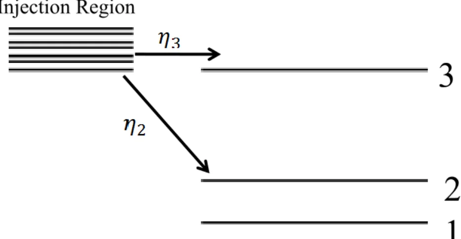
Up to now, quantum cascade laser is analyzed by quantum mechanics with microscopic properties. However some macroscopic quantities such as threshold current density and slope efficiency can be analyzed without having to quantum mechanics. These quantities can be derived in a very simple rate equation approach.
Consider simple rate equation analyses of a single active region only. Let active region have 3 energy states and assume that laser action happened in between state 3 and 2 and state 1 is just state that enhance relaxation of level 2. Also assume that there is injector state with constant population 𝑛𝑔. Schematic illustration of
this system is presented in Figure 2.4.
Figure 2.4 Rate equation model illustration
Before writing rate equations, some assumptions should be made;
1. Assume scattering from level 1 to injector is very fast, which means lifetime in level 1 is zero.
2. Electrons are injected in state 3 at rate 𝐽 𝑒⁄ and injection is only through state 3, injection to state 2 is forbidden, which means injection efficiency is 100 %.
3. Injector consist of only one level with constant electron density 𝑛𝑔
Injector
Injector
1
2
3
33
4. Lifetime of state 3 is 𝜏3−1= 𝜏32−1+ 𝜏31−1+ 𝜏𝑒𝑠𝑐, 𝜏𝑒𝑠𝑐 is lifetime of electron escape process state 3 to continuum.
5. Assume electrons can thermally activated from injector to state 2 and thermally activated number of electrons at thermal equilibrium is 𝑛2𝑡𝑒𝑟𝑚.
Rate equations for one active region period are;
𝑑𝑛3 𝑑𝑡 = 𝐽 𝑒− 𝑛3 𝜏3 − 𝑆𝑔𝑐(𝑛3− 𝑛2), (2.62) 𝑑𝑛2 𝑑𝑡 = 𝑛3 𝜏32+ 𝑆𝑔𝑐(𝑛3− 𝑛2) − (𝑛2−𝑛2𝑡𝑒𝑟𝑚) 𝜏2 , (2.63) 𝑑𝑆 𝑑𝑡= 𝑐0 𝑛𝑟[𝑆(𝑔𝑐(𝑛3 − 𝑛2) − 𝛼𝑡𝑜𝑡) + 𝛽 𝑛3 𝜏𝑠𝑝]. (2.64)
where S is photon flux per period, 𝑔𝑐 is gain cross section, 𝛼𝑡𝑜𝑡 is total modal loss
and 𝛽 is spontaneous emission overlap factor to laser mode. 𝑛2𝑡𝑒𝑟𝑚 is ;
𝑛2𝑡𝑒𝑟𝑚 = 𝑛𝑔𝑒−∆𝑘𝑇. (2.65)
where ∆ is energy difference between state 2 and Fermi level of injector region. 𝑔𝑐 is gain cross section which is;
𝑔𝑐 = 𝛤 4𝜋𝑒2
ε0nʎ0L |z32|2
2𝛾 . (2.66)
where 𝛤 is overlap factor, z32 is dipole matrix element L is length of period and 𝛾 is broadening of the laser transition.
34
Below threshold, to find steady state solution equates derivatives and S to zero and neglect spontaneous emission (since lifetime is too long) obtain;
∆𝑛 = (𝑛3− 𝑛2) = 𝐽𝜏3 𝑒 (1 − 𝜏2 𝜏32) − 𝑛2 𝑡𝑒𝑟𝑚. (2.67)
and it is know that at the threshold modal gain is equal to the loss 𝑔𝑐∆𝑛=𝛼𝑡𝑜𝑡
So threshold current is;
𝐽𝑡ℎ = (𝑒 𝑔𝑐 𝛼𝑡𝑜𝑡+ 𝑛2 𝑡𝑒𝑟𝑚) 1 𝜏3(1−𝜏2⁄𝜏32) , (2.68) More explicitly; 𝐽𝑡ℎ= 1 𝜏3(1−𝜏2⁄𝜏32)[ ε0nʎ0L2𝛾 4𝜋𝑒2𝛤|z 32|2𝛼𝑡𝑜𝑡+ 𝑒𝑛2 𝑡𝑒𝑟𝑚]. (2.69)
Above the threshold to find steady state solution equate all derivatives ((2.62), (2.63) and (2.64)) to zero. Photon flux (S) is obtained as;
𝑆 = (𝐽(𝜏3(1−𝜏2⁄𝜏32))−𝑒𝛼𝑡𝑜𝑡⁄𝑔𝑐)
𝑒𝛼𝑡𝑜𝑡(𝜏3(1−𝜏2⁄𝜏32)+𝜏2) =
(𝐽−𝐽𝑡ℎ)𝜏3(1−𝜏2⁄𝜏32)
𝑒𝛼𝑡𝑜𝑡(𝜏3(1−𝜏2⁄𝜏32)+𝜏2) . (2.70)
Also to obtain slope efficiency take derivative of S over J;
𝑑𝑆
𝑑𝐽 =
𝜏3(1−𝜏2⁄𝜏32)
𝛼𝑡𝑜𝑡(𝜏3(1−𝜏2⁄𝜏32)+𝜏2). (2.71)
Therefore slope efficiency (derivative of optical output power over applied current to the device) of the device is;
𝑑𝑃
𝑑𝐼 = 𝑁𝑝ħω𝛼𝑓1 𝑑𝑆
35
where 𝑁𝑝 is number of period of the device 𝛼𝑓1 is front mirror loss.
2.6. Gain Medium Design and Modeling
The quantum cascade design has to overcome interrelated problems:
Population inversion between upper and lower laser state has to be achieved
Laser threshold gain has to overcome waveguide losses. Structure has to be electrically stable at bias point.
First demonstration of the quantum cascade laser that solved these problems is published in 1994 by J. Faist et.al milestone work [22].
Generally, in order to solve these problems quantum cascade laser structure are divided two parts; active region where laser action occurs and injection/relaxation region where electrons carried to following period of cascaded structure.
In simplest case, active region consist of at least three energy states; laser action occurs between third and second state, this model can be model with three level pumping schemes [23]. To satisfy population inversion, third energy level lifetime is adjusted to be longer then lower states’ lifetime.
Injection/relaxation regions consist of minibands and minigaps, which is realized by sequence of alternating quantum wells and barriers. Main purpose of these regions is enabling resonant tunneling to deplete lower state and pumping adjacent upper state.
Also some layers of these regions are doped to serve as electron reservoir and to prevent arising space charge regions.
The most attractive feature of quantum cascade laser is cascading [3]. Active region and injection/relaxation region can be connected consecutively. Theoretically a single electron is able to stimulate number of photon in cascading process. Conduction band diagram of first quantum cascade laser is in Figure 2.5.
36
Figure 2.5 Conduction band diagram of first quantum cascade laser [7].
2.6.1. Active Region Design
Active region is the most important part of the quantum cascade laser, since entire laser action happened in this region. According to (2.69) and (2.71) high efficient and robust active region should have following properties:
Long upper state lifetime Short lower state lifetime Low waveguide loss
Narrow transition line width Large optical matrix element
Low thermally activated electrons to fill lower states (low thermal backfilling)
As expected, it is not possible to satisfy all of these properties at the same time Upper state lifetime and optical matrix element is inversely correlated. In other words, in order to increase optical matrix element, spatial overlap between wave functions in upper and lower laser states have to be increased, however as spatial overlap between states increases, lifetime between states decreases. Therefore optimum value between lifetime and matrix element should be adjusted or designs
![Figure 1.1 Figure 1.1 a) Graphical representation of the location of strong absorptions of molecules [1] b) Illustration of infrared countermeasures of an aircraft [2]](https://thumb-eu.123doks.com/thumbv2/9libnet/5878726.121279/18.892.195.767.194.751/graphical-representation-location-absorptions-molecules-illustration-infrared-countermeasures.webp)
![Figure 2.9 Computed transition of superlattice structure with 3 and 5 number of periods [3]](https://thumb-eu.123doks.com/thumbv2/9libnet/5878726.121279/57.892.273.680.206.522/figure-computed-transition-superlattice-structure-number-periods.webp)